© 2019, IRJET | Impact Factor value: 7.211 | ISO 9001:2008 Certified Journal
| Page 5817
Design and Simulation of Comparator Architectures for Various ADC
Applications
Disha Gaude
1, Bathini Poornima
2, K. M. Sudharshan
3, Prashant V. Joshi
41,2,3,4
Dept. of Electronics and communication Engineering, REVA University, Bengaluru, India
---***---Abstract - This paper presents design and simulation of different CMOS comparators. The designs are simulated and studied in 180 nm Technology with Cadence Virtuoso Tool with supply voltage 3.3 V and reference voltage of 3V. The clock used in comparator has a frequency of 1 M Hz. The comparators are mostly used in converting analog signals to digital signals for processing. Comparators are used in the applications requiring less power dissipation, good accuracy and high resolution.
Key Words: comparator, Dynamic, Static, Latch, Clock Frequency, Pre amplifier, post amplifier.
Ⅰ. Introduction
Comparator is a circuit which compares two input voltages in which one is analog input and other is reference voltage and outputs binary 0 or 1 depending on comparison. It is basically a 1 bit analog to digital converter. In ADCs sample and hold circuit samples the analog input signal and the sampled signal is given to comparator, depending on reference voltage it produces digital output which is equivalent to analog input signal [1].
[image:1.595.312.534.418.564.2]Comparators are used in all ADCs requiring less power dissipation, high speed, low noise, less offset voltage, good slew rate etc. Different types of comparators are available namely open loop comparator, regenerative comparator and combination of both open loop and regenerative comparator (cascaded comparators) [2]. Open loop compactors are basically single and two stage differential amplifiers without compensation and feedback loop. Regenerative comparators use positive feedback to improve the performance [3]. Comparator circuits can also be built by separating the comparators into number of cascaded stages. This helps in reducing the total propagation delay time and hence can be used in high speed applications like radar receivers and LAN interfaces.
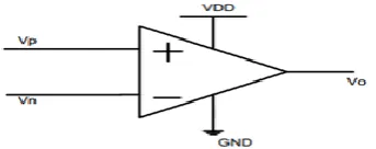
Fig -1. Symbol of comparator
Above figure shows the symbol of comparator. It is basically operational amplifier because every comparator has one or many of the same characteristics as a high gain amplifier. The voltage Vp applied to the positive terminal of the comparator gives output 1 if voltage Vn applied to negative terminal is less or equal to Vp or else the output of the comparator gives 0 [11].
Ⅱ. Characterization of a comparator
Static characteristics
Gain
The ideal aspect of this model is the way in which the output makes a transition between VOL and VOH. The output changes states for an input change of ΔV, where ΔV approaches zero [4]. The gain is given as
[image:1.595.75.247.667.735.2]Gain = AV =
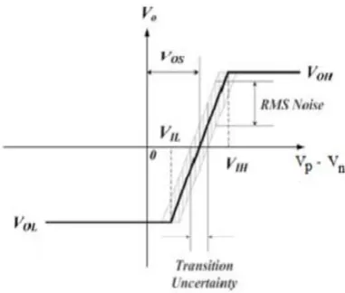
Fig -2. Ideal transfer curve
Offset Voltage
© 2019, IRJET | Impact Factor value: 7.211 | ISO 9001:2008 Certified Journal
| Page 5818
Fig -3. Transfer curve of a comparator including offset voltage and noise
Dynamic characteristics
Propagation Delay
Propagation delay is defined as at how much speed the amplifier responds with applied input [6].
Propagation delay time = (rising propagation delay time + falling propagation delay time)/2
Fig -4. Propagation delay curve
Ⅲ Comparator Topologies
A. Two stage open loop comparator
Comparator requires differential input and high gain to achieve desirable resolution. As a result two stage operational amplifiers can be used as a comparator. Comparator requires large bandwidth as possible so that faster response can be achieved. This is done by making two stage operational amplifiers as an open loop mode, thus no compensation is required [7].The advantage of this comparator is to provide high gain, large output voltage swing and disadvantage is that it consumes more
[image:2.595.323.541.130.291.2]power. Hence, it is not suitable for high speed and low power applications.
Fig -5. Open loop comparator
Small signal gain of the comparator as given by
AV = ( ) ( )
Two stage comparator consists of two pole, first and second stage output poles P1 and P2 respectively are given as
P1 = -
Where CI is the sum of capacitance connected to the output of first stage.
P2 =
Where CII is the sum of capacitance connected to the output of second stage.
B. Regenerative comparator
Regenerative comparators use positive feedback to accomplish the comparison of two signals. The regenerative comparator is also called a latch or bistable. The simplest form of a latch is shown below
[image:2.595.57.264.426.569.2] [image:2.595.336.528.624.733.2]© 2019, IRJET | Impact Factor value: 7.211 | ISO 9001:2008 Certified Journal
| Page 5819
[image:3.595.313.557.115.254.2]Normally, the latch has two modes of operation. The first mode disables the positive feedback and applies the input signal to the terminals as V01 and V02. The initial voltages applied during this mode will be as V011 and V012. The second mode enables the latch and depending on the relative values of V011 and V012, one of the outputs will go high and the other will go low. A two phase clock is used to determine the modes of operation [10].
Fig -7. Dynamic latch
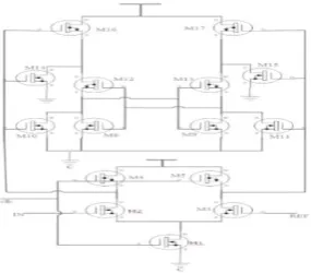
C. High speed comparator
High speed comparators should have a propagation delay time as small as possible. To achieve this goal, one must understand the requirement for fast comparator. This is best understood by separating the comparator into a number of cascading stages. So, this three cascading stages consists of input pre amplification stage, latch stage and output post amplification stage [8].
Pre amplification stage consists of current mirror single stage differential amplifier with high gain and low slew rate. This stage improves sensitivity of the comparator by isolating input from kickback noise and amplifying the smallest minimum input voltage. Latch is basically positive feedback circuit which determines the difference of the two input signals. Post amplification stage consists of self-biased differential amplifier followed by inverter. This stage helps in driving the high load and inters parasitic capacitance [9].
Fig -8. High speed comparator
Ⅵ Simulation Results
[image:3.595.87.230.204.329.2]Fig -9. Schematic of two stage uncompensated comparator
[image:3.595.314.554.283.442.2]Fig -10. Output waveforms of two stage uncompensated comparator
Fig -11. Schematic of dynamic latch
[image:3.595.59.264.615.752.2]© 2019, IRJET | Impact Factor value: 7.211 | ISO 9001:2008 Certified Journal
| Page 5820
[image:4.595.54.269.239.405.2]Fig -13. Schematic of high speed comparator
Fig -14. Output waveforms of comparator
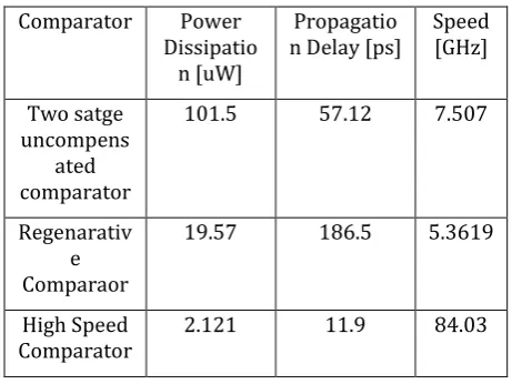
Table -1. Comparision of different types of comparator parameters
Comparator Power Dissipatio
n [uW]
Propagatio
n Delay [ps] Speed [GHz]
Two satge uncompens
ated comparator
101.5 57.12 7.507
Regenarativ e Comparaor
19.57 186.5 5.3619
High Speed
Comparator 2.121 11.9 84.03
Ⅴ. Conclusion
In this paper two stage uncompensated comparator, dynamic latch, regenerative comparator and high speed comparator with cascaded stages are implemented and simulated and simulation is carried out using Cadence tools, with gpdk 180nm. It is also verified with LT-SPICE using tsmc180nm technology file. The power dissipation, total propagation delay and speed are compared and
calculated for different types of comparators with supply voltage 5 V.
Ⅵ. Acknowledgement
I am extremely thankful to Dr. Rajashekhar C Biradar, Director of the school of Electronics and Communication Engineering, Prof. Prashanth V Joshi coordinator, Mr. H. G. Yatheesh from VLSI industry for their valuable guidance and useful suggestions to work effectively with my project.
References
[1] S. Kim and K. Kwon, "A hybrid ADC combining capacitive DAC-based multi-bit/cycle SAR ADC with flash ADC," 2016 International Conference on Electronics, Information, and Communications (ICEIC), Da Nang, 2016.
[2] U. M. Kulkarni, C. Parikh and S. Sen, "A Systematic Approach to Determining the Weights of the Capacitors in the DAC of a Non-binary Redundant SAR ADCs," 2018 31st International Conference on VLSI Design and 2018 17th International Conference on Embedded Systems (VLSID), Pune, 2018.
[3] W. Kim et al., "A 0.6 V 12 b 10 MS/s Low-Noise Asynchronous SAR-Assisted Time-Interleaved SAR (SATI-SAR) ADC," in IEEE Journal of Solid-State Circuits, vol. 51, no. 8, pp. 1826-1839, Aug. 2016.
[4] C. Liu, M. Huang and Y. Tu, "A 12 bit 100 MS/s SAR-Assisted Digital-Slope ADC," in IEEE Journal of Solid-State Circuits, vol. 51, no. 12, pp. 2941-2950, Dec. 2016.
[5] S. Lee, A. P. Chandrakasan and H. Lee, "A 1 GS/s 10b 18.9 mW Time-Interleaved SAR ADC With Background Timing Skew Calibration," in IEEE Journal of Solid-State Circuits, vol. 49, no. 12, pp. 2846-2856, Dec. 2014.
[6] V. P. Singh, G. K. Sharma and A. Shukla, "Power efficient SAR ADC designed in 90 nm CMOS technology," 2017 2nd International Conference on Telecommunication and Networks (TEL-NET), Noida, 2017.
[7] S. Z. Hoseini and K. Lee, "Compact Time-Mode SAR ADC With Capacitor Flipping Bit-Cycling Operation," 2018 IEEE 61st International Midwest Symposium on Circuits and Systems (MWSCAS), Windsor, ON, Canada, 2018.
[8] A. Bekal, M. Goswami, B. R. Singh and D. Pal, "A Low Power 8-Bit Asynchronous SAR ADC Design Using Charge Scaling DAC," 2014 Fifth International Symposium on Electronic System Design, Surathkal, 2014.
[image:4.595.46.277.469.642.2]© 2019, IRJET | Impact Factor value: 7.211 | ISO 9001:2008 Certified Journal
| Page 5821
[10] Yin, G. M., Eynde, F. O., & Sansen, W. (1992). A high-speed CMOS comparator with 8-bit resolution. IEEE Journal of Solid-State Circuits.
[11] Donadkar, D. N., & Bhandari, S. U. (2015). Review on Comparator Design for High Speed ADCs. 2015 International Conference on Computing Communication Control and Automation.
[12] Babayan-Mashhadi, S., & Lotfi, R. (2014). Analysis and Design of a Low-Voltage Low-Power Double-Tail Comparator. IEEE Transactions on Very Large Scale Integration (VLSI) Systems.
[13] Vinodiya, S. K., & Gamad, R. S. (2017). Analysis and design of low power, high speed comparators in 180nm technology with low supply voltages for ADCs. 2017 8th International Conference on Computing, Communication and Networking Technologies (ICCCNT).
[14] Fouzy, B. B. A., Reaz, M. B. I., Bhuiyan, M. A. S., Badal, M. T. I., & Hashim, F. H. (2016). Design of a low-power high-speed comparator in 0.13μm CMOS. 2016 International Conference on Advances in Electrical, Electronic and Systems Engineering (ICAEES).