© 2019, IRJET | Impact Factor value: 7.211 | ISO 9001:2008 Certified Journal | Page 3064
Performance Estimation of FIR Filter using Null Convention Logic
Toushiba Khan
1, Dr. S.R.P. Sinha
21M.tech Scholar, Department of Electronics Engineering, Institute of Engineering and Technology
2Professor, Lucknow, Dr. APJ Abdul Kalam Technical University Lucknow India 226021
---***---Abstract
- An asynchronous delay insensitive NullConvention Logic (NCL) with dual rail signal has been used to design an improved low power high speed FIR filter and presented in this paper. NCL reduces the dynamic power consumption by reducing the switching activity. The power delay product of FIR filter using both conventional and NCL CMOS model has been estimated and compared in 90 nm technology with a frequency of 250MHz at 1.2V. Power reduction of 22% is achieved for the supply voltage of 2.5V in NCL CMOs model compared to conventional CMOS model
Key Words: Null conventional logic, asynchronous delay insensitive, Dynamic Power
1. INTRODUCTION
The development in the field of communication engineering and technology has identified the research to design low power and high speed FIR filters using the variety of concepts. The filters play a major role in the field of communication, radar, biomedical signal processing and video processing as the electronic industry is growing rapidly. Filtering is a class of signal processing, which defines the complete or partial suppression of some aspects of the signal. It removes some unwanted frequencies in order to suppress interfering signals and reduces background noise. Filters may be digital or analog filter. In digital filter, FIR filter play a vital role in the performances such as modification, reshaping and manipulation of the frequency spectrum of signal according to the desired requirements. Moreover, FIR filters are the important building blocks because of their linear phase and stability. FIR filter has a finite number of input samples which affects the generation of a given output sample and it is a time-invariant discrete linear system, frequently used in Digital Signal Processing system by virtue of stability and easy implementation. It performs the frequency shaping or the linear prediction on a discrete-time input sequence {x0, x1, x2…}.The output is obtained as a sum of delayed and scaled input samples. An LTI system interacts with its input signal
through a process called linear convolution. The convolved sequence is given by
y[n] = x[n]* h[n] (1)
y n
∑
h
kx n
−
k
(2)where h[n] is the impulse response, x[n] is the input signal and y[n] is the output signal
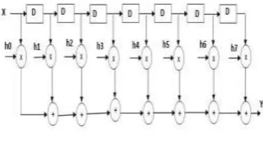
The FIR filter shown in Fig.1 consists of adders, multipliers and delay elements. The output can be obtained by multiplying the delayed inputs and the coefficients as given in (1).
[image:1.595.350.539.386.490.2]
Figure 1 Structure of fir filter
The power dissipation of FIR filter depends up on the number of transistors in adders, multipliers and delay elements. The power dissipation is due to three sources: static power dissipation, dynamic power dissipation and short circuit power dissipation. Low power dissipation will allow the system to operate longer with the same battery. Power consumption in a logic network depends on system clock frequency (f), switching activity (Pi), size of transistor and their capacitance ( Ceq), supply voltage (VDD), short-circuit current (ISC) and leakage current (IL) , as given in (3).
P=∑ VDD V swing C eq f Pi + VDD ∑ I sc + V DD IL (3)
10-© 2019, IRJET | Impact Factor value: 7.211 | ISO 9001:2008 Certified Journal | Page 3065 transistor full adder and the conventional 28-transistor
CMOS adder. The disadvantage of the new adders is the threshold-voltage loss of the pass transistors. An advanced version of spurious power suppression technique (SPST) on multipliers for high-speed and low-power purposes have been proposed by Kuan-Hung Chen and Yuan-Sun Chu [2].It leads to a 40% speed improvement. The developed SPST-equipped multiplier dissipates 0.0121 mW per MHz in 0.18µm CMOS technology and obtained 40% power reduction. Oscal T.C. Chen et.al [3] has designed a power-efficient digital signal processor by developing a low-power adder which operates on effective dynamic data ranges. The 32-bit adder used has reduced the power dissipation in multimedia applications. Besides the ripple adder, the developed processor utilized in other adder cells, such as carry lookahead and carry-select adders to compromise complexity, speed and power consumption for application-specific integrated circuits and digital signal processors
2-Fir filter Design Using NCL
Null Convention logic (NCL) provides an asynchronous design methodology employing dual rail signals [6], to incorporate data and control information into one mixed path. This logic is a symbolically complete logic which expresses in terms of the logic itself. NCL aims at designing VLSI devices with greater ease, with reduced power budget, lower electromagnetic interference effects and reduced noise margins. The circuits using NCL utilize dual-rail or quad-rail logic to achieve delay-insensitivity [7] –[9].
A dual-rail signal, D, consists of two wires, D0
and D1, which may assume any value from the set {DATA0, DATA1, NULL}. The DATA0 state (D0 = 1, D1 = 0) corresponds to a Boolean logic 0,the DATA1 state (D0 = 0, D1 = 1) corresponds to a Boolean logic 1, and the NULL state (D0 = 0, D1 = 0) corresponds to the empty set which means that the value of D is not yet available. The two rails are mutually exclusive, such that both rails can never be asserted simultaneously. This state is defined as an illegal state. Both dual-rail and quad-rail signals are space optimal 1-hot delay-insensitive codes, requiring two wires per bit.
NCL circuits have been constructed using threshold gates with hysteresis for its composable logic elements. One type of threshold gates is the THmn gate, where 1 ≤ m ≤ n as depicted in Fig. 2. A THmn gate corresponds to an operator with at least m signals
[image:2.595.332.528.314.368.2]asserted in set condition and all signals de-asserted before the output becomes asserted. Hysteresis is used to provide a means for monotonic transition and a complete transition of multi –rail signals back to NULL state before asserting the output associated with the next wave front of input data [10]. In a THmn, each of the n inputs is connected to the rounded portion of the gate. The output emanates from the pointed end of the gate. The gate’s threshold value m, is written inside of the gate. Another type of gate is weighted threshold gate denoted as THmnWw1w2…wR in Fig. 2. Weighted threshold gates have an integer value, m ≥ wR > 1, applied to input R. Here 1 ≤ R < n; where n is the number of inputs; m is the gate’s threshold; and w1, w2, …wR, each > 1, are the integer weights of input1, input2, …input R, respectively.
Figure 2- Symbol of Threshold gates
A- Transistor level implementation of NCL gates NCL threshold gates are designed with hysteresis state-holding capability, such that after the output is asserted, all inputs are deasserted before the output is deasserted. NCL gates have both set and hold equations, where the set equation determines when the gate will remain asserted and the hold equation determines when the gate will remain asserted once it has been asserted. The set equation determines the gate’s functionality, where as the hold equation is the same for all the NCL gates and is simply all inputs ORed together. The general equation for an NCL gate with output Z is Z=Set + (Z - * hold), where Z- is the previous output value and Z is the new value. NCL gates can be implemented using static CMOS and semi static CMOS implementation [5]. NCL gate using CMOS technology can be implemented by complement of Z , which in general form is :Z’=reset + (Z- ‘ * set’), where reset is complement of hold (either complement of each input, ANDed together),such that the gate is deasserted when all input are deasserted and remains deasserted while the gate’s set condition is false.
B- Basic gates using NCL
© 2019, IRJET | Impact Factor value: 7.211 | ISO 9001:2008 Certified Journal | Page 3066 and X1=0. If the input X is logic 1 then it can be encoded
as X0=0 and X1=1 C- Adders using NCL
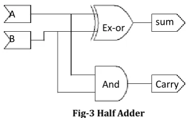
Half adder: Half Adder has been designed usingthe
[image:3.595.50.243.202.323.2]EX-OR gate and AND gate which is designed using NCL gates as ahown in Fig.3.
Fig-3 Half Adder
Full Adder: A full adder has been designed usingtwo
[image:3.595.341.525.367.515.2]half adders and an OR gate as shown in Fig. 4.
Fig-4 Full adder
D. Multiplier using NCL-Multiplier has been designed using the AND gates, half adders and full adders designed using NCL. D-Flip flop: D-Flip flop consists of NAND gates and inverter designed using NCL where the output is obtained during the application of high clock pulse.
E. FIR Filter using NCL- An 8 tap Filter has been designed using AND gates, Full adders, 16 bit Ripple carry adder, 8x8 array multiplier and D-flip flops. 3. Results and discussion-The 8 tap low pass FIR filter using NCL CMOS model has been designed and implemented using HSPICE and DSCH in 90nm technology.
In TH23 gate, the reset equation is ABC and the simplified set equation is AB+BC+AC. Directly
implementing these equations for Z and Z', after simplification, yields the static transistor-level implementation of an NCL gate as shown in Fig. 6 for TH23 gate. This requires the output to be feedback as an input to the NMOS and PMOS L OGIC to achieve hysteresis behavior.
Half adder:Half Adder has been designed as in
Fig. 8 using the NCL gates and it is optimized using Threshold Combinational Reduction method. When either A0 or B0 is asserted C0 will be asserted which is implemented using TH12 gate. C1 asserts output data only when A1 and B1 asserts data. S1 asserts output data when C0 asserts data with either A1 asserts data input value or B1 asserts data input value but not both at same time. Hence S1 is designed using TH33w2 gate where C0 will be input with more weight than others S0 asserts output data when C1 asserts data orA0 and B0 asserts data input. The sum and carry is given in table 1
FIGURE 6: HALF ADDER USING NCL
Inputs
X0 X1 Y0 Y1 1 0 1 0 1 0 0 1 0 1 1 0 0 1 0 1
Outputs
S0 S1 C0 C1
1 0 1 0
0 1 1 0
0 1 1 0
[image:3.595.30.267.373.518.2]1 0 0 1
Table-1 NCL half adder
Full Adder: From the truth table, optimized equation are Co1 = A1B1 + Ci1A1 + Ci1B1 and Co0 = A0B0 + Ci0 A0 +Ci0B0. Both functions can directly be mapped in to TH23 gate as shown in Fig. 9. The Karnaugh – map for Sum output S is based on A,
A
B Ex-or
And
sum
Carry ++++ ++++ ++++ ++++ ++++ ++++ ++++ ++++ ++++ ++++ ++++ ++++ ++++ ++++ ++++ ++++ ++++ ++++ ++++ ++++ ++++ ++++ ++++ ++++ ++++ ++++ ++++ ++++ ++++ ++++ ++++ ++++ ++++ ++++ ++++ ++++ A
OR
HA LF; F
HA
A
B
sum
Carry
[image:3.595.314.555.543.689.2]© 2019, IRJET | Impact Factor value: 7.211 | ISO 9001:2008 Certified Journal | Page 3067 Band Ci along with output from Co. S0 = Co1A0 +
[image:4.595.310.567.59.301.2]Co1B0 + Co1 Ci0 + A0B0Ci0and S1 = Co0A1 + Co0B1+Co1 Ci0 + A1B1 Ci0, both are directly mapped intoTH34w2 gates where Co has more weight than the other input in Table 2.
FIGURE 6: Full adder using NCL
INPUTS
A
0 A1 B0 B1 Ci Ci 1
1 0 1 0 1 0
1 0 1 0 0 1
1 0 0 1 1 0
1 0 0 1 0 1
0 1 1 0 1 0
0 1 1 0 0 1
0 1 0 1 1 0
0 1 0 1 0 1
OUTPUTS
S
0 S1 C0 C1
1 0 1 0
0 1 1 0
0 1 1 0
1 0 0 1
0 1 1 0
1 0 0 1
1 0 0 1
[image:4.595.42.284.181.422.2]0 1 0 1
Table 3- NCL Full Adder
Table 3 shows the comparison of FIR filter designed using NCL logic with conventional CMOS logic. Low power and high speed has been obtained compared to conventional CMOS logic.
Table 4 Comparison of conventional CMOS with NCL logic for 8 Tap FIR filter
Parameters Conventional
CMOS logic NULL convention Logic
Transistor counts 27950 72465
Power
consumption(mW) 26.9 20.8
Delay(ns) 32.8 30.7
Area(nm2) 0.587034 1.52166
Power delay
product(J) 0.8768×10
-9 0.63648×10⁻⁹
0.8 1 1.2 1.4 SCL 20 20.2 21 22 NCL 12.2 14 16 18
0 5 10 15 20 25
P
ow
e
r
di
ss
ipa
ti
on(m
W
)
supply voltage(V)
4- Conclusion-The 8 tap FIR Filter using conventional CMOS and NCL CMOS model have been implemented and analyzed. The FIR filter using NCL achieves high speed and low power dissipation compared with conventional CMOS model. The power delay product is better when compared with the conventional CMOS model. The power dissipation for different supply voltages and operating frequencies were estimated and found that NCL CMOS model outperform the conventional CMOS model.
REFERENCES
1. Hung Tien Bui, Yuke Wang, and Yingtao Jiang, “Design and Analysis of Low-Power 10-Transistor Full Adders Using Novel XOR–XNOR Gates”, IEEE Trans on Circuits and Systems—II: Analog and Digital Signal Processing, Vol. 49, No. 1, January 2002
2. Kuan-Hung Chen and Yuan-Sun Chu, “A Low-Power Multiplier with the Spurious Low-Power Suppression Technique”, IEEE Trans. on Very Large Scale Integration (VLSI) Systems, Vol. 15, No. 7, July 2007
3. Oscal T.-C. Chen, Robin Ruey-Bin Sheen and Sandy Wang,” A Low-Power Adder Operating on Effective Dynamic Data Ranges” IEEE Trans. on Very Large Scale Integration (VLSI) Systems, Vol. 10, No. 4, August 2002
© 2019, IRJET | Impact Factor value: 7.211 | ISO 9001:2008 Certified Journal | Page 3068 5. Montek Singh, Jose A. Tierno, Alexander
Rylyakov, Sergey Rylov, and Steven M. Nowick,” An Adaptively Pipelined Mixed Synchronous-Asynchronous Digital FIR Filter Chip Operating at 1.3 Gigahertz”, IEEE Trans. on Very Large Scale Integration (VLSI) Systems, Vol. 18, No. 7, July 2010 1043
6. Hauck.S, ”Asynchronous Design Methodologies :An overview “, Proceeding of the IEEE,vol.83, No:1, pp69-93, 1995
7. Scott C. Smith, “ Design of an FPGA Logic Element for Implementing Asynchronous NULL Convention Logic Circuits”, IEEE Trans. on Very Large Scale Integration (VLSI) Systems, Vol. 15, No. 6, June 2007.
8. J. Sparso, J. Staunstrup, and M. Dantzer-Sorensen, “Design of delay insensitive circuits using multi-ring structures,” in Proc. Eur. Design Autom. Conf., 1992, pp. 15–20
9. Gerald E.Sobelman and Karl M.Fant, ”CMOS circuit design of threshold gates with Hysteresis” IEEE International symposium on circuits and systems (II) ,pp.61-65, 1998. 10. David, R. Ginosar, and M. Yoeli, “An efficient
implementation of boolean functions as self-timed circuits,” IEEE Trans. Comput., vol. 41, no. 1, pp. 2–10, Jan. 1992.