University of Warwick institutional repository:http://go.warwick.ac.uk/wrap
A Thesis Submitted for the Degree of PhD at the University of Warwick
http://go.warwick.ac.uk/wrap/73546
This thesis is made available online and is protected by original copyright. Please scroll down to view the document itself.
Magnetotransport, structural and optical characterization
ofp-type modulation doped heterostructures with
high Ge content Si1-xGex channel grown
by
SS-MBE on
Si1_yGey/Si(OOl) virtual substrates
BY
MAKSYM MYRONOV
Thesis submitted in partial fulfilment of the requirements for the degree of
Doctor of Philosophy in Physics
TABLE OF CONTENTS
Table of contents
List of figures and tables Acknowledgements Declaration
Abstract
List of abbreviations
1. Introduction
2.
1.1 Impact of SiGe on Si microelectronics References
Theoretical concepts and review of previous works 2.1 Structural and electronic properties of bulk Si and Ge
2.1.1 Energy band structure 2.1.2 Carriers effective mass 2.1.3 Carriers mobility
2.2 The strained Sit-xGex/Sh-yGey heterostructures 2.2.1 Energy band alignment in heterostructures 2.2.2 Strain adjustment in heterostructures
2.2.3 Strain relaxed Sit-yGey ISi(OOI) buffer layers
2.2.4 Layers sequence in modulation doped Sh-xGex/Sh-yGey heterostructures 2.3 Transport properties of 2DHG formed in the Sh-xGex channel of
p-type modulation doped heterostructures
page
1 5
6 6 6 8 II 15 15 20 22 27
3.
2.3.2 Carriers scattering mechanisms
2.3.2.1 Background impurity scattering 2.3.2.2 Remote impurity scattering 2.3.2.3 Interface-roughness scattering 2.3.2.4 Alloy scattering
2.3.2.5 Acoustic-phonon scattering 2.3.2.6 Optical-phonon scattering
2.3.2.7 Threading dislocations scattering
2.3.3 Carriers transport in p-type modulation doped Sit-xGex/Si1-yGey heterostructures
2.3.4 Carriers transport in magnetic field: Classical approach 2.3.4.1 Mobility spectrum approach
2.3.4.2 Maximum-entropy mobility spectrum analysis 2.3.5 Carriers transport in magnetic field: Quantum approach
2.3.5.1 20 carriers in magnetic field 2.3.5.2 Shubnikov-de Haas effect 2.3.5.3 Quantum Hall Effect References
Experimental methods
3.1 Solid source molecular beam epitaxy 3.2 Transmission electron microscopy 3.3 Secondary ion mass spectrometry 3.4 Photoluminescence spectroscopy 3.5 Raman spectroscopy
3.6 Scanning white-light interferometry
3.7 Devices fabrication for magnetotransport measurements 3.7.1 Van der Pauw device
3.7.2 Hall-bar devices
3.8 Cryostats equipment and operations
3.8.1 Closed-cycle cryostat system (9-300K) 3.8.2 Cryomagnetic system (O.35-300K) 3.9 Resistivity and Hall measurements
3.9.1 Van der Pauw device 3.9.2 Hall-bar device References
4. Design, growth and annealing procedure of p-type MOD Sit-xGe,/Sit-yGey heterostructures
4.1 Design ofp-type MOD Sit-xGex!Sit-yGey heterostructures
4.2 The p-type MOD Sit-xGex/Sit-yGey heterostructures investigated in current research
4.3 Post growth thermal annealing treatments on p-type MOD Si t-xGex/Si t-yGey heterostructures
S. Results and discussions of structural and optical analysis of p-type MOD Sit-xGex/Sit-yGey heterostructures
5.1 Introduction
5.2 Transmission electron microscopy analysis of p-type MOD Sit-xGex/Sit_yGey heterostructures 5.3 Secondary ion mass spectrometry analysis of
67 67 68 69 69 70 72 73 74 75
76 76
80
86
88
885.4
Photoluminescence spectroscopy analysis of
p-type MOD Sh-xGex/Sh-yGey heterostructures
5.5
Raman spectroscopy analysis of
p-type MOD Sit-xGex/Sit-yGey heterostructures
5.6
Scanning white-light interferometry analysis of
p-type MOD Sh-xGexlSi1-yGey heterostructures
5.7
The effect of post growth furnace and rapid thermal annealing on structural
and optical properties ofp-type MOD Sh-xGex/Sit-yGey heterostructures
5.8
The effect ofGe composition in the Si1-xGex channel and
Sit_yGey layers on structural and optical properties of
p-type MOD Sit_xGex/Sit-yGey heterostructures
5.9
Conclusions
References
6. Results and discussions of magnetotransport characterization of p-type MOD Sit-xGex/Sit_yGey heterostructures
6.1
Magnetotransport properties ofp-type MOD Sil-xGexlSil-yGey heterostructures
measured at temperatures
9-300K
6.1.1
Introduction
6.1.2
Results and discussion
6.1.2.1
The effect of post growth furnace thermal annealing
on magnetotransport properties ofp-type MOD
Si l-xGex/Si l-yGey heterostructures
6.1.2.2
The effect of post growth rapid thermal annealing
on magnetotransport properties of p-type MOD
Si l-xGex/Si l-yGey heterostructures
97
103
113
118
119
122
124
126
126
126
127
143
6.1.2.3 The effect ofGe composition in the Sil-xGex channel and Sil-yGey layers on magnetotransport properties of
p-type MOD Sil-xGex/Sh-yGey heterostructures 6.1.3 Conclusions
150 153 6.2 Room temperature magnetotransport properties of 2DHG formed in the Sil-xGex
channel ofp-type MOD Sil-xGex!Sh-yGey heterostructures: Maximum-entropy mobility spectrum analysis
6.2.1 6.2.2 6.2.3
Introduction
Results and discussion Conclusions
156 156 156 159 6.3 Low temperatures (down to 0.35K) magnetotransport properties of 2DHG formed in
the Sil-xGex channel ofp-type MOD Sil-xGex/Sh-yGey heterostructures:
Shubnikov-de Haas and Quantum Hall Effects 165
6.3.1 Introduction 165
6.3.2 Results and discussion 165
6.3.3 Extraction of sheet carrier density and mobility of 2DHG 171 6.3.4 Extraction of effective mass and related parameters of 2DHG 176
6.3.5 Conclusions 182
References 184
LIST OF FIGURES AND TABLES
FIGURES
Figure 2.1 Energy band structures of Ge and Si, where Eg is the indirect energy bandgap. Plus (+) signs indicate holes in the valence bands and minus (-) signs indicate electrons in the conduction bands [3].
Figure 2.2 Band gap variation of Sh-xGex alloys against Ge content x. The top curve gives the band gap energy for unstrained (cubic) alloys, which show a crossover from the Si-like (conduction band minima at L\) to the Ge-like bandstructure (conduction band minima at the L point) at x=O.85. The two other curves are for pseudomorphic Sh-xGex layers on a cubic Si substrate, which leads to a splitting of the valence band [4].
Figure 2.3 (a) Conduction-band offsets Ecmin(x)_Ecmin(y) and (b) valence-band offsets Ey1llQX(x)_Eymax(y) in eV at interface ofa lattice matched (001) strained Sh-xGex alloy and an unstrained (cubic) Sh-yGey bulk substrate (after [7]).
Figure 2.4 Critical thickness versus composition for Si1-xGex on Si. The lowest curve gives the theoretical limit in thermal equilibrium [29], whereas the experimental curve is for a metastable layer grown at 550C by MBE.
Figure 2.5 Layer sequences typically employed for (a) pseudomorphic p-type MOOQWs with Si1-xGex channel, (b) p-MOOQWs with Ge-rich Si1-xGex (or pure Ge) channel on relaxed Si1_yGey buffer layer, and (c) n-MOOQWs with Si channel on relaxed Si1-yGey buffer layer.
page
7
7
18
21
28
Figure 3.1 Van der Pauw cross sample: a) resistivity measurements b) Hall effect 73 measurements.
Figure 3.2 Hall-bar sample: a) resistivity measurements b) Hall effect measurements. 74 Figure 4.1 Variations of sheet carrier density versus spacer width at B doping 1·1Q18cm-3, 2·1Q18cm-3, 4·1Q18cm-3 and 8·1018cm-3 for p-type MOD Sio.2Geo.slSio.7Geo.3 77 heterostructure calculated using self-consistent solution of 10 Poisson-Schrodinger equations.
Figure 4.2 Energy band diagram and carriers distribution at 10K for p-type MOD Sio.2Geo.slSio.7Geo.3 heterostructure calculated using self-consistent solution of 10 78 Poisson-Schrodinger equations.
Figure 4.3 Temperature dependence of mobility of 2DHG formed in the Sio.2Geo.s channel of p-type MOD Sio.2Geo.slSio.7Geo.3 heterostructure calculated with relaxation 79 time approximation theory of carriers' transport. Also shown the variation of mobility with temperature for each scattering mechanism taken in isolation.
Figure 4.6 Schematic vIew of #622.54, #622.55 and #622.56 p-type MOD 83 heterostructures.
Figure 4.7 Schematic view of#622.83 and #622.84 p-type MOD heterostructures. 84 Figure 4.8 Schematic view of #C1957, #C1987, #C2015f and #C2072 p-type MOD 85 heterostructures.
Figure 4.9 Schematic view of#C2475 and #C2476 p-type MOD heterostructures. 86 Figure 5.1 XTEM images of Sio.2Geo.8 channel region (top) and all grown layers 89 (bottom) of as-grown sample #60.46.
Figure 5.2 XTEM images of Sio.2Geo.8 channel region in as-grown (top) and after FTA 90 at 750C for 30min (bottom) samples #60.46.
Figure 5.3 XTEM images of Sio.2Geo.8 channel region (top) and all grown layers 92 (bottom) of as-grown sample #622.83.
Figure 5.4 ULE-SIMS profiles ofGe (top) and B (bottom) in Si1-xGex channel region of 95 as-grown and after FTA at 750C for 30min samples #60.46.
Figure 5.5 ULE-SIMS profiles ofGe (top) and B (bottom) in Sh-xGex channel region of 96 samples #60.45 and #60.46.
Figure 5.6 PL spectra measured at 5.5K from as-grown and after FTA at 600C, 700C 99 and 750C for 30min samples #60.46.
Figure 5.7 PL spectra measured at 5.5K from as-grown sample #622.54. 100 Figure 5.8 PL spectra measured at 5.5K from as-grown and after FTA at 600c, 750C 101 and 900C for 30min samples #622.83.
Figure 5.9 PL spectra measured at 5.5K from samples #1957 and #1987. 102 Figure 5.10 Room temperature Raman spectra of as-grown sample #60.46 excited with 107 488nm light.
Figure 5.11 Room temperature Raman spectra of as-grown and after FTA at 700c and 108 750C for 30min samples #60.46 excited with 488nm light.
Figure 5.12 Room temperature Raman spectra of as-grown sample #622.83 excited with 109 457.9nm, 488nm and 514.5nm light.
Figure 5.13 Room temperature Raman spectra of as-grown and after FTA at 600c, 110 700C, 750C, 800C and 900C for 30min samples #622.83 excited with 514.5nm light.
Figure 5.14 FTA effect on position and intensity of Ge-Ge modes in room temperature III Raman spectra of sample #622.83 excited with 514.5nm light.
Figure 5.16 Scanning white-light interferometry surface profiles of sample #51.33 115 analysed by Metro Pro software.
Figure 5.17 Scanning white-light interferometry surface profiles of sample #60.46 115 analysed by Metro Pro software.
Figure 5.18 Scanning white-light interferometry surface profiles of sample #622.54 116 analysed by Metro Pro software.
Figure 5.19 Scanning white-light interferometry surface profiles of sample #622.83 116 analysed by Metro Pro software.
Figure 5.20 Scanning white-light interferometry surface profiles of sample #C 1957 117 analysed by Metro Pro software.
Figure 5.21 Scanning white-light interferometry surface profiles of sample #C2072 117 analysed by Metro Pro software.
Figure 6.1 Temperature dependences of Hall mobility and sheet carrier density for as- 134 grown sample #51.33 and after FTA at 600C, 700C, 800C and 900c for 30min.
Figure 6.2 Temperature dependences of Hall mobility and sheet carrier density for as- 135 grown sample #52.16 and after FTA at 600C, 700C, 800C and 900C for 30min.
Figure 6.3 Temperature dependences of Hall mobility and sheet carrier density for as- 136 grown sample #54.08 and after FTA at 600C, 700C, 800C and 900C for 3Omin.
Figure 6.4 Temperature dependences of Hall mobility and sheet carrier density for as- 137 grown sample #60.46 and after FT A at 600C, 700C, 750C and 800C for 30min.
Figure 6.5 Temperature dependences of Hall mobility and sheet carrier density for as- 138 grown sample #622.83 and after FTA at 600C, 700C, 750C, 800C and 900C for 30min. Figure 6.6 Temperature dependences of Hall mobility and sheet carrier density for as- 139 grown sample #622.84 and after FTA at 600C, 700C, 750C, 800C and 900C for 3Omin. Figure 6.7 Temperature dependences of Hall mobility and sheet carrier density for as- 140 grown sample #C1987 and after RTA at 750C for 30min.
Figure 6.8 Temperature dependences of Hall mobility and sheet carrier density for as- 141 grown sample #C2072 and after RTA at 750C for 30min.
Figure 6.9 Temperature dependences of Hall mobility and sheet carrier density for as- 142 grown samples #CI957, #C2475 and #C2476.
Figure 6.10 FT A effect on Hall mobility and sheet carrier density of 2DHG formed in the channel of samples #51.33, #52.16, #54.08, 60.46, #622.83 and #622.84 measured at 146 9K.
Figure 6.12 MEMS (top) as the result of O'xx and O'xy fit (bottom) measured at 221K for 161 sample #60.46 after FTA at 750C for 30min.
Figure 6.13 MEMS (top) as the result ofO'xx and O'xy fit (bottom) measured at 290K for 162 sample #60.46 after FTA at 750C for 30min.
Figure 6.14 Temperature dependences of drift mobility and sheet carrier density (0) of 2DHG formed in the Sit.xGex channel obtained with the help ofMEMSA, and measured
by combination of resistivity and Hall effect techniques Hall mobility and sheet carrier density (.) at 290K for sample #60.46 after FTA at 750C for 30min.
163
Figure 6.15 MEMS (top) as the result of O'xx and O'xy fit (bottom) measured at 293K for 164 sample #C1957.
Figure 6.16 Magnetic field dependences of magneto resistance (top) and Hall resistance (bottom) measured at 0.35K on as-grown and after FTA at 700C for 30min samples 166 #622.83.
Figure 6.17 Magnetic field dependences of magneto resistance (top) and Hall resistance (bottom) measured at 0.346-24.5K temperatures on the sample #622.83 after FTA at 168 700C for 30min.
Figure 6.18 Magnetic field dependences of magnetoresistance (top) and Hall resistance (bottom) measured at 0.34S-S,47K temperatures on the sample #C2072 after RTA at 169 750C for 30sec.
Figure 6.19 Magnetic field dependences of magneto resistance (top) and Hall resistance 170 (bottom) measured at 0.356-20.715K temperatures on the sample #C1957.
Figure 6.20 Measured SdH oscillations (top) and SdH oscillations without monotonous 174 part (bottom) for sample #C1957 at T=0.356K.
Figure 6.21 SdH oscillations in inverse magnetic field (top) and their FFT spectrum 175 (bottom) for sample #C1957 at T=0.356K.
Figure 6.22 Amplitudes of SdH oscillations (liM1) as a function of magnetic field at given temperatures (top) and amplitudes of SdH oscillations (liMB» as a function of 178 temperature at given magnetic fields (bottom) for sample #C1957.
TABLES
Table 2.1 Selected structural parameters of unstrained bulk silicon and germanium at room temperature [2].
Table 2.2 Experimental band parameters of unstrained, undoped bulk Si and Ge at room temperature.
mo
is the free electron mass. Note that the effective masses are band-edge masses, which apply only for low-doped structures at low electric fields. (Data from [2]).Table 2.3 Room-temperature bulk mobilities of electrons and holes in unstrained, undoped Si and Ge (from [2]).
Table 2.4 Deformation potentials [7], spin-orbit splittings
L\o
and elastic constants CII and Cl2 for Si and Ge [2].6
9
14
19
Table 6.1 Hall mobility and sheet carrier density of 2DHG formed in the channel of as-grown and after RTA at 750C for 30sec samples #CI987, #C2015f, #C2072 measured 148 at9K.
Table 6.2 Hall mobility and sheet carrier density of as-grown and after RTA at 750C for 149 30sec samples #CI987, #C2015f, #C2072 measured at 293K.
Table 6.3 Hall mobility and sheet carrier density of 2DHG formed in the Sit-xGex channel of as-grown and after optimum thermal annealing samples #51.33, #52.16, #54.08, #60.46, #622.54, #622.83, #622.84, #CI957, #CI987, C2015f, #C2072, #C2475, #C2476 measured at 9K.
151
Table 6.4 Hall mobility and sheet carrier density of as-grown and after optimum thermal annealing samples #51.33, #52.16, #54.08, #60.46, #622.54, #622.83, #622.84, #CI957, 153 #CI987, C2015f, #C2072, #C2475, #C2476 measured at 293K.
Table 6.5 Room temperature drift mobility and sheet carrier density of 2DHG formed in the Sit-xGex channel obtained by MEMSA and measured by combination of resistivity and Hall effect techniques Hall mobility and sheet carrier density for samples #60.46 after FTA at 7S0C for 30min, #C2072 after RTA at 750C for 30sec and #CI957.
Table 6.6 Resistivity, Hall mobility and sheet carrier density of 2DHG at 0.3SK extracted from magnetic field dependences of magnetoresistance and Hall resistance for samples 622.83 after FTA at 700C for 30min, #C2072 after RTA at 750C for 30sec and #CI957.
158
173
ACKNOWLEDGEMENTS
I would like to thank my supervisors Professor E.H.C. Parker and Professor T.E. Whall for their valuable guidance throughout my PhD course. I am very grateful to Dr. O.A. Mironov for his everyday supervision, fruitful discussions and his technical expertise throughout the magnetotransport characterization phase of my research. My thanks to Dr. C.P. Parry and Dr. P.J. Phillips for SS-MBE growth of samples that have been studied in my research and useful discussions. To all my other colleagues from Advanced Semiconductors Research group (Department of Physics, University of Warwick, Coventry, UK), both past and present. I would like to thank Dr. S.G. Lyapin and Dr. P.C. Klipstein from Clarendon Laboratory (Department of Physics, University of Oxford, Oxford, UK) for 3 years of our collaboration, which consisted of Raman spectroscopy and Photoluminescence measurements of SiGe heterostructures, and very useful discussions. I would like to thank Dr. U. Konig and members of his group from Daimler Chrysler AG Research and Technology (VIm, Germany) for our collaboration. In particular to Dr. T. Hackbarth for SS-MBE growth of SiGe heterostructures and Dr. G. Hoeck for supply of samples and useful discussions. The great thanks to those people with whom were discussed the experimental results obtained during this research, their teaching and advising. Especially to Professor R.A. Stradling and Dr. J.J. Harris (Imperial College of Science, Technology and Medicine, London, UK), Professor E.B. Yakimov (Institute of Microelectronics Technology, Russian Academy of Sciences, Chemogolovka, Russia), Professor V.G. Kantser (International Laboratory of SSE, Academy of Sciences, Kishinev, Moldova), Professor A.G. Cullis (University of Sheffield, Sheffield, UK) and Professor M.G. Dowsett (University of Warwick, Coventry, UK).
DECLARATION
This thesis is the result of research carried out by the author in Department of Physics, University of Warwick, UK between December 1997 and December 2000 and is submitted as partial fulfilment of the requirements for the award of the degree of Doctor of Philosophy in Physics. The work described here is all my own, except where acknowledged as otherwise in
the text.
A large amount of the performed work during this research has been published in scientific journals and presented at the international scientific conferences.
Publications in journals during this research
1. M. Myronov, c.P. Parry, T.E. Whall and E.H.C. Parker "Annealing effect on transport and structural properties of Si).xGex/Sh.yGey/Si(OOI) p-type modulation doped heterostructures" submitted to Applied Physics Letters
2. M. Myronov, C.P. Parry, O.A. Mironov, T.E. Whall and E.H.C. Parker "Very high hole mobility in Sio.2Geo.slSio.6sGeo.3sISi(001) p-type MOD metamorphic heterostructures" submitted to Applied Physics Letters
3. S. Kiatgamolchai, O.A. Mironov, V.G. Kantser, M. Myronov, E.H.C. Parker, T.E. Whall, Z. Dziuba "Maximum Entropy Mobility Spectrum Analysis for Electron Transport in Layered Semiconductor Structures" submitted to Physical Review B. 4. Yu.F. Komnik, V.V. Andrievskii, LB. Berkutov, S.S. Kryachko, M. Myronov and
T.E. Whall "Quantum effects in the hole-type Si/SiGe heterojunctions". Low Temperature Physics, Vo1.26, NS, pp.609-614, 2000.
publications in conference proceedings during this research
1. O.A. Mironov, M. Myronov, E.H.C. Parker, T.E. Whall "High Ge content SiGe MODFET heterostructures on virtual substrates for device applications: HOLE MOBILITIES higher than electrons in the room temperature range of operation". Abstract book: "SiGe (C) 2001 Workshop", 21-23 January 2001, Tohoku University, Sendai, Japan, p.V-02.
3. M. Myronov, C.P. Parry, O.A. Mironov, E.H.C. Parker, O.A. Soltanovich and E.B. Yakimov "Growth and annealing induced defects analysis in Si1_xGex/Sit_yGeylSi(001) heterostructures with high Ge content". Abstract book: "International Conference on Solid State Crystals 2000: Materials Science and Applications", 2-13 October 2000, Zakopane, Poland, p.69.
4. M. Myronov, S. Kiatgamolchai, O.A. Mironov,l T.E. Whall, E.M. Sheregii, G. Tomaka, T. Kakol, J. Klamut "Mobility spectrum analysis of high Ge content SiGe/Si heterostructures". Abstract book: "International Conference on Solid State Crystals 2000: Materials Science and Applications", 2-13 October 2000, Zakopane, Poland, p.140.
5. M. Myronov, E.H.C. Parker, T.E. Whall, S.G. Lyapin, P.C. Klipstein "Thennal annealing effect on properties of Sio.2Geo.slSio.7Geo.3/Si(001) p-type modulation doped heterostructures". Abstract book: "10th European Heterostructure Technology Workshop", 18-19 September 2000, University of Ulm, International Institute Schloss Reisensburg, Gunzburg, Gennany, p.31.
6. M. Myronov, C.P. Parry, O.A. Mironov, E.H.C. Parker, T.E. Whall, E. Hoeflinger, G. Bauer "Post-growth annealing effect on magnetotransport and structural properties of Sio.2Geo.slSio.6sGeo.3sISi(00 1) modulation doped heterostructure". Abstract book: "10th European Heterostructure Technology Workshop", 18-19 September 2000, University ofUlm, International Institute Schloss Reisensburg, Gunzburg, Gennany, p.57.
7. G. Hoeck, T. Hackbarth, M. Myronov, O.A. Mironov, E.H.C. Parker, E. Kohn "Magnetotransport properties of Sit-xGex/Sit_yGeylSi(OOI) p-type modulation doped heterostructures with high Ge content channel". Abstract book: "10th European Heterostructure Technology Workshop", 18-19 September 2000, University of UIm, International Institute Schloss Reisensburg, Gunzburg, Gennany, p.35.
8. S. Kiatgamolchai, M. Myronov, O.A. Mironov, E.H.C. Parker, T.E. Whall "A Novel Mobility Spectrum Maximum Entropy Approach for Magnetotransport Analysis of SiGe/Si heterostructures". Abstract book: "10th European Heterostructure Technology Workshop", 18-19 September 2000, University ofUlm, International Institute Schloss Reisensburg, Gunzburg, Gennany, p.65.
9. M. Myronov, S.G. Lyapin, C. Parry, E.H.C. Parker, T.E. Whall, P.C. Klipstein, J.M. Bonar "Post-growth annealing effect on properties of p-type modulation doped Sio.2Geo.slSio.6sGeo.3sISi(001) heterostructure studied by XTEM and Raman spectroscopy". Abstracts book: "CMMP'99", 19-22 December 1999, University of Leicester, Leicester, UK, SEMd.P 1.21.
10. S. Kiatgamolchai, M. Myronov, E.H.C. Parker, T.E. Wha11, J.C. Yeoh, T.K. Fobelets, T.J. Thornton "Mobility Spectrum of 2DHG and 2DEG in SiGe-Si Heterostructures". Abstracts book: "11th General Conference of the European Physical Society (EPS-II): Trends in Physics", 6-10 September 1999, Church House Conference Centre, London, UK, p.53.
ABSTRACT
This thesis is a report on experimental investigations of magnetotransport, structural and optical properties ofp-type modulation doped (MOD) heterostructures with Sit-xGex channel of high Ge content (0.6<x<l) grown on Sit_yGey/Si(OOI) virtual substrate (VS). The active layers of MOD heterostructures were grown by solid source molecular beam epitaxy (SS-MBE). The VSs were grown either by SS-MBE or low-pressure chemical vapour deposition (LP-CVD).
The influence of thermal annealing on magnetotransport, structural and optical properties of Sit-xGexlSit-yGey heterostructures was studied by performing the post growth furnace thermal annealing (FTA) treatments in the temperature range of 600-900C for 30min and rapid thermal annealing (RTA) treatments at temperature 750C for 30sec.
Structural and optical analysis of p-type MOD Sit-xGex!Si1-yGey heterostructures involved the techniques of cross-sectional transmission electron microscopy, ultra low energy secondary ion mass spectrometry, photoluminescence spectroscopy, micro-Raman spectroscopy and scanning white-light interferometry. From the combinations of experimental results obtained by these techniques the Ge composition in the SiGe heteroepilayers, their thicknesses, state of strain in the heteroepilayers and dislocations microstructure in VSs were obtained.
After post growth thermal annealing treatments were observed broadening of the Si1-xGex channel accompanied with the reduction of Ge content in the channel and smearing of Sit-xGex/Sit_yGey interfaces.
The Sio.7Geo.3 on low-temperature Si butTer VSs with very good structural properties were designed and grown by SS-MBE. These include: relatively thin 850nm total thickness of VS, 4-6nm Peak-to-Valley values of surface roughness, less than lOscm-2 threading dislocations density and more than 95% degree of relaxation in the top layers ofVS.
The Hall mobility and sheet carrier density of as-grown and annealed p-type MOD Sit-xGex/Sil-yGey heterostructures were obtained by a combination of resistivity and Hall etTect measurements in the temperature range of 9-300K. The FTA at 600C for 30min was seen to have a negligible etTect on the Hall mobility and sheet carrier density. Increasing the annealing temperature resulted in pronounced successive increases of Hall mobility accompanied by the opposite behaviour of sheet carrier density. Each sample had the optimum FTA temperature corresponded to the maximum Hall mobility. After RTA at 750C for 30sec the increase of Hall mobility for researched samples was observed as well. The highest mobility (at sheet carrier density) of 2DHG measured at 9K was observed for sample containing Ge channel grown on thick Sio.4Geo.6 linearly graded VS and corresponds to 14855cm2.y-I·s-l (2.87. 10 1 2cm-2). The highest Hall mobility (at sheet carrier density) measured at 293K was observed for Sio.2Geo.slSio.6sGeo.3s heterostructure after FT A at 750C for 30min and corresponds to 1776cm2.y-I·s-t (2.37·1013cm-2).
To extract the drift mobility and sheet carrier density of 2DHG at temperatures up to 300K, magnetotransport measurements in magnetic fields up to II T were performed on several heterostructures. The data were analyzed by technique of Maximum-Entropy Mobility Spectrum Analysis. The highest drift mobility (at sheet carrier density) of2DHG at 290K was obtained for the Sio.2Geo.slSio.6sGeo.3s heterostructure after FTA at 750C and corresponds to 3607 cm2·V-I·s-1 (4.94.1012cm-2).
2DCG 2DEG 2DHG CMOS CVD DOS FET HH I-QMSA LH LP-CVD LT-Si MBE MEMSA MOD MODQW MOSFET MSA QMSA
SdH
SO SOlList of abbreviations
Two dimensional carrier gas Two dimensional electron gas Two dimensional hole gas
Complementary metal oxide semiconductor Chemical vapour deposition
Density of states Field effect transistor Heavy-hole
Improved quantitative mobility spectrum analysis Light-hole
Low pressure chemical vapour deposition Low-temperature Si
Molecular beam epitaxy
Maximum-entropy mobility spectrum analysis Modulation-doping
Modulation doped quantum well
Metal oxide semiconductor field effect transistor Mobility spectrum analysis
Quantitative mobility spectrum analysis Shubnikov-de Haas
Spin-orbit-split hole Si-on-insulator
SS-MBE Solid source molecular beam epitaxy UHV Ultra high vacuum
UHV -CVD Ultra high vacuum chemical vapour deposition VLSI Very large-scale integration
1. Introduction
1.1 Impact of SiGe on Si microelectronics
While the first transistor was fabricated using germanium in 1947 [1] and III-V semiconductor materials have consistently demonstrated superior high-speed performance, it is silicon that completely dominates the present semiconductor market. At present, the vast majority of all semiconductor devices produced on production lines are used the Si-based technologies. One may put forward many subtle and non-subtle reasons for this position but there is one that dominates all, - cost. It is clear that the silicon complementary metal oxide semiconductor (CMOS) field effect transistors (FETs) have an advantageous position compared to III-V-based transistors with costs in 1999 being over 200 times cheaper than GaAs per square millimeter. The low cost of CMOS may be traced to the ability to fabricate billions of transistors all with near identical properties across slices of silicon of ever-increasing diameter. The fabrication processes and the device performance rely heavily on a number of natural properties of silicon, but the most important reason for the unrivaled success of Si devices lies in the combination of an easily available semiconductor and an excellent natural oxide, namely Si02, which serves as an insulator and as a protecting passivation layer. Si02 have allowed Si to dominate over faster materials such as GaAs because for these alternative and more expensive fabrication schemes must be used, which cannot reach the phenomenal yields achievable on a CMOS line. The increase in density and performance of CMOS has been produced by down-scaling the transistors and circuits over the years. The gate-lengths of the transistors in circuits have followed an exponential scaling law since the first metal oxide semiconductor FET (MOSFET) was produced in the early 1960s [2]. The exponential decrease in size has been termed Moore's law after Gordon Moore, who first analyzed the effect. While this decrease in size has allowed an increase in density and a decrease in cost per transistor, the cost of fabrication plants has also been scaling upwards at an exponential rate [3]. At some
point, however, this scaling must finish, whether fundamental or economic, will eventually appear to prevent smaller transistors or circuits being fabricated. With the amount of capital and knowledge presently tied up in both Si production and research, the impetus to design and produce devices in Si is enormous. With present production plants costing in excess of $100 billion, it is almost impossible to persuade companies to change to completely new, untried technologies. CMOS is so cheap and dominant that one must find applications where it cannot be used, such as optoelectronics, analogue or high-speed markets, if a new technology is to appear on the market place. One compromise is to use a new material system that is CMOS compatible, such as SiGe, to allow bandgap-engineered devices with higher performance or new functionality [4]. One may suggest that this is going back to the roots of the original Ge transistor by adding Ge to the system, but the SiGe is strained, which completely changes the material and electronic properties along with the physics. Increased integration levels reduce the number of chips in final products and hence should lower costs and increase yields. SiGe has the advantage that it may be used to modify conventional transistors to give higher speed and lower power. The Semiconductor Industry Association roadmap [5] predicts that conventional, CMOS transistors cannot operate below gate lengths of order of 70 nm while the use of SiGe in conventional FET devices has been predicted to allow smaller dimensions. Coupled to this the ability to produce quantum devices on the same chip gives SiGe substantial potential for future circuits.
but they differ to a large enough extent to allow selective structuring procedures. These obvious advantages of a Si-based all-group-IV heterosystem were recognized at an early stage of heterostructure research, with the first report on a Sit-xGe,/Si superlattices appearing already back in 1975 [6].
One of the main problems in growing Sit-xGex alloy on a Si(OOI) substrate is the lattice mismatch, which increases from 0 to 4.2% as x is varied from 0 to 1. The larger x becomes, the thinner the Sit-xGex channel has to be grown in order to prevent misfit dislocations from relaxing the strain. Hence if Ge is grown on Si then only 4 atomic mono layers may be grown before the energy from the strain in the system creates dislocations. There is therefore a critical thickness, above which defects in the form of dislocations are produced if a strained layer is grown too thick. One of the possibilities to obtain Ge compositions x>O.5, while retaining strain in the Sit-xGex layer, is to use relaxed Si1-yGey substrate with the bulk lattice constant of the Sit-yGey. This allows strained Si, Ge or Sit-xGex to be grown on an underlying Si wafer. Such substrates are termed virtual substrates (VSs).
Nevertheless, progress in material growth and basic understanding of the band alignment lagged initially behind similar investigations made in the much more popular, lattice-matched GaAs/ AIGaAs heterosystem. With growth techniques, such as molecular beam epitaxy (MBE), then still in their infancy, a main reason can be seen in the quite significant lattice mismatch between Si and Ge, but also in severe doping problems caused by the strong segregation of most dopants then available. Over the years, most of the growth and doping problems have been solved, and the understanding of the strain effects induced by the lattice mismatch has reached a state that allows their exploitation as a further parameter in the field of man-made bandstructures.
An example for the high level reached in the last years is the Sit-xGex/Si heterobipolar transistor [7] (HBT), with demonstrated cut-off frequencies and maximum
oscillation frequencies well beyond
100
GHz [8,9]. This is roughly a factor-of-two improvement as compared to the best existing Si bipolar junction transistors (BJTs), but, what is more important, the Sit-xGex/Si HBT boosts Si-based technologies into an area that has so far been a exclusive domain of 111-Y devices.At present, the HBT is the most advanced device type in the Sit-xGex/Si heterosystem, with products having already been announced, or being expected to be available commercially in the very near future [10]. In addition, a variety of other potential applications are pursued by the ever-increasing number of research groups working in the field of Si-based heterostructures. As an example, optoelectronic functions including infrared detectors and waveguides, and even light emitters, are investigated intensely [11].
Since the aforementioned Si-MOSFETs are the most widespread of all electronic devices, a successful introduction of the Sit-xGex/Si heterostructure into that mainstream area is expected to have an enormous impact. Referring to the experiences gained with Ill-y MODFETs, the advantages a hetero-MOSFET can offer are obvious: at room temperature the carrier mobility can be increased by a factor of two to three by employing the band offset at the Sit-xGex/Si heterojunction to spatially separate the mobile carriers from the ionized dopants on the one side, and from the interface with the Si02 insulator on the other side. This will provide the hetero-MOSFET with higher operation frequencies without sacrificing its intrinsic very large-scale integration (VLSI) ability. Enhanced electron and hole mobilities are not only important for future device applications; they can also provide new insights in the transport properties of low-dimensional carrier gases. The low-temperature electron mobility in the Si channel of a modulation-doped quantum well structure (MODQW) has recently been driven to a value beyond 500,000 cm2
.y.
lJ.1m. This is large enough to conduct experiments on quantum point contacts and in the mesoscopic range, which so far were mainly restricted to high-mobility III-V heterostructures. Enhanced hole mobilities are another topic, which will become even more exciting, because the recently demonstrated realization of high Ge content Sh-xGex channels allows unprecedented high hole mobilities.
References:
1. Bardeen J., W. H. Brattain, Phys. Rev. 1948, 71, 230.
2. Kahng D., in Semiconductor Devices: Pioneering Papers (Ed: S. M. Sze), World Scientific, Singapore 1991, p. 583.
3. The National Technology Roadmap for Semiconductors, Semiconductor Industry Association, San Jose, CA 1997.
4. People R., IEEE J. Quantum Electron. 1986, QE-22, 1696.
5. The National Technology Roadmap for Semiconductors, Semiconductor Industry Association, San Jose, CA 1997.
6. Kasper E., H.J. Herzog and H. Kibbel1975 Appl. Phys. 8199
7. Gruhle A. 1994 Silicon-Based Millimeter-Wave Devices (Springer Series in Electronics and Photonics
32)
ed J-F Luy and P Russer (Berlin:Springer) ch 48. Crabbe E. et a/1993 Tech. Digest 51st Device Research Conf. (New York: IEEE) 9. Schuppen A., A. Gruhle, H. Kibbel, U. Erben and U. Konig 1994 IEDM Tech. Digest
1994 (New York: IEEE) p 377
10. Kerrmarec C., T. Tewksburry, G. Dawe, R. Bains, B.S. Meyerson, D. Harame and M. Gilbert 1994 Microwave J. 3722
11. Presting H., H. Kibbel, M. Jaros, R.M. Turton, U. Menczigar, G. Abstreiter and H.G. Grimmeiss 1992 Semicond. Sci. Technol. 7 1127
12. Ismail K., M. Arafa, K.L. Saenger, J.O. Chu and B.S. Meyerson 1995 Appl. Phys. Lett. 66 1077
2. Theoretical concepts and review of previous works
2.1 Structural and electronic properties of bulk Si and Ge
2.1.1 Energy band structure
Silicon and germanium are the only group-IV elements that are completely miscible, i.e. they form a continuous series of solid substitutional solutions with gradually varying properties over the entire composition range. The elements and the random Si1-xGex alloys crystallize in the cubic diamond lattice with a lattice parameter that increases almost linearly [1] with x. The maximum mismatch amounts to 4.2% between pure Si and pure Ge. The fundamental band gap in both Si and Ge is indirect (Table 2.1), and remains so for all compositions in the Sh-xGex alloys. The conduction band minima are six-fold degenerate in Si, where they are located along the [100] directions near the X point (usually referred to as L\ minima), and eightfold degenerate in Ge, where they are located at the Brillouin-zone boundary in the [111] directions (L minima) (Figure 2.1). The crossover between these two types of band structure occurs at x=0.85 in unstrained (i.e. cubic) Sh-xGex alloys. The indirect bandgap at 300K (4.2K) decreases monotonically from 1.11 e V (1.17 e V) to 0.66e V (0.7 4e V) as the Ge content x increases from 0 to 1. A distinct kink occurs at the crossover point (top curve in Figure 2.2). The most important structural parameters [2] are listed in Table 2.1.
Table 2.1 Selected structural parameters of unstrained bulk silicon and germanium at room temperature [2].
Silicon (Si) Germanium (Ge)
Lattice type Diamond Diamond
Lattice constant, a (A) 5.431 5.657
Direct bandgap, Ella (e V) 3.40 0.80
Indirect bandgap, Egi (eV) 1.11(L\) 0.664(L)
~ Ge
3
-!
r;
t GI:E9
W
1&1 0
-1
-3
-4~---~--~---L [Itt]
r
[100]x
L [ttl]r
[100] XFigure 2.1 Energy band structures of Ge and Si, where Eg is the indirect energy bandgap. Plus (+) signs indicate holes in the valence bands and minus (-) signs indicate electrons in the conduction bands [3].
1.1
-~
~1.0co C)
>-~0.9
Q)
0.8
0.2
0.4
1.0Ge content x (%)
Figure 2.2 Band gap variation of Sil-xGex alloys against Ge content x. The top curve gives the band gap energy for unstrained (cubic) alloys, which show a crossover from the Si-like (conduction band minima at ~) to the Ge-like bandstructure (conduction band minima at the L point) at
x=O.85.
The two other curves are for pseudomorphic Sit-xGex layers on a cubic Si substrate, which leads to a splitting of the valence band [4].The bandgap variation is strongly affected by strain in the Sil-xGex crystal, a situation that occurs in most of the thin-film applications. To illustrate the span of energy gaps accessible, the lower two curves in Figure 2.2 show the bandgap variations of Sh-xGex alloys grown pseudomorphically on an Si(lOO) substrate. Under these conditions the in-plane lattice constant of the substrate is conserved throughout the alloy layer, which leads to a tetragonal distortion of the film according to the elastic properties of the lattice. Two curves exist because of the strain-induced heavy-hole/light-hole splitting of the valence band maximum [4]. Evidently, the main effects of the compressive in-plane strain are a significant and monotonic reduction of the indirect bandgap with increasing x, and a suppression of the aforementioned crossover from the Si-like to a Ge-like band structure. Experimental bandgap data are so far only available for unstrained bulk alloys and for pseudomorphic Sh-xGex films on Si substrates. For the latter case, which is technologically important (e.g. for the SiiSiGe HBT) the data points agree well with the calculated bandgap variations. The more general case of fully strained Sh-xGex layers on a relaxed
Sit_yGey substrate has been treated theoretically by several authors; however, their results differ quite substantially, due to the different methods used in the calculations [5].
2.1.2
Carriers effective mass
Table 2.2 Experimental band parameters of unstrained, undoped bulk Si and Ge at room temperature. mo is the free electron mass. Note that the effective masses are band-edge masses, which apply only for low-doped structures at low electric fields. (Data from [2]).
Silicon Germanium
Electron mass (mo) mt 0.19 0.08
ml 0.91 1.59
A -4.26 -13.27
Valence band parameters B -0.63 -8.63
lei
4.93 12.4mhh 0.53 0.28
Band-edge masses of hole (mo) mlh 0.15 0.04
mso 0.23 0.09
In both materials the longitudinal mass is significantly larger than the transversal mass. Measured electron masses in bulk Si and Ge showed that the conduction band minima behave to good approximation parabolic, i.e. the mass parameters are only weakly affected by band-filling effects via temperature or doping [6]. No experimental data on the electron masses in unstrained Sh-xGex alloys are available. However, theoretical investigations suggest that A (Si-like) and L (Ge-like) mass parameters remain almost unaffected over the entire range of compositions, and that they are also rather insensitive to strain [7]. Thus, the main effect of (uniaxial) strain on the conduction band minima is the experimentally verified lifting of the respective degeneracy.
The situation at the valence band edge is even in the elemental semiconductors more complex, because the
r
-point valence band maximum is made up of three strongly interacting bands. In unstrained Si and Ge the heavy-hole (HH) and light-hole (LH) bands (rs+ symmetry) are degenerate at the r point, whereas the spin-orbit-split hole (SO) band (r7+ symmetry) is separated by ASi=44 meV in Si and Aoe=290 meV in Ge [2]. The rs+ bands are warped, i.e. the effective masses depend on the crystal direction. In a first approximation the band dispersion is frequently described by the three band parameters A, B, ande
according to(2.1)
(2.2)
where Ev is the r-point energy,
mo
is the free electron mass, !l. is the spin-orbit splitting, and h is Planck's constant. The+
and - signs describe the LH and HH bands, which splitfor k* O. The parabolic approximation in (2.1) is only valid next to the r point. The close proximity of the bands leads also to a significant non-parabolicity, especially of the HH band, even for minor changes of the hole energy. As a result, the effective hole masses depend sensitively on external electric fields as well as on doping concentration and temperature. Hence the experimental values of the three hole masses for Si and Ge given in Table 2.2 apply only to small hole densities and are averaged values over all crystal directions.
Experimental and theoretical works concerning the valence bands in Sit-xGex alloys have been performed by several groups. It was found that a linear interpolation of the SO splitting between the values of Si and Ge agrees reasonably well with experimental results conducted on Sit-xGex bulk alloys [8]. On the other hand, the variation of the band parameters with x, and thus of the effective hole masses, is the subject of much more controversial discussions. Most of the calculations or interpolation schemes employing the band parameters A, B, and C, or other sets of band parameters derived from the different matrix representations of the valence band, failed to reproduce all experimental data available. At least qualitative agreement of the x dependence has been achieved by the non-linear interpolation scheme proposed by Lawaetz [9].
Application of strain lifts the degeneracy of the HH and LH bands at the r point [10].
band can have a lower mass than the lower-lying LH band. This class of layer sequences corresponds to biaxial compressive strain in the (100) plane concomitant with uniaxial tensile strain perpendicular to this plane. The strain components are reversed, if a pseudomorphic Sh-xGex layer is grown on cubic Sh-yGey with x<y. Accordingly, the LH is shifted up while simultaneously its effective mass becomes heavy-hole-like.
2.1.3 Carriers mobility
The most important transport parameter of a semiconductor material and device is the carrier mobility. The mobility depends very much on the manner in which it is measured and it is important to understand the mobility determined by a particular characterization method and method's limitations. The carrier mobility, influences the device behavior through its frequency response or time response in two ways. First, the carrier velocity is proportional to the mobility for low electric fields. Hence higher mobility material is likely to have a higher frequency response, because carriers take less time to travel through device. Second, the device current depends on the mobility, and higher mobility materials have higher current. Higher currents charge capacitances more rapidly, resulting in a higher frequency response. There are several mobilities in use [12]:
• Microscopic mobility
is the fundamental mobility calculated from basic concepts. It describes the mobility of the carriers in their respective band.e f.J=_.'C'
m*
(2.3)where e is the electron charge, 'C' is transport scattering time and
m*
is the effective mass of the respective carrier. Within the limits of the wave-vector-independent relaxation time approximation ,-1 is the sum of all reciprocal scattering times associated with the various scattering mechanisms (Mathiessen's rule). Thus the mobility is limited by the mechanism with the smallest scattering time.• Hall mobility is determined from the combination of conductivity and Hall effect measurements.
(2.4) where RH is Hall coefficient for low magnetic fields and Gis conductivity.
• Drift mobility is the mobility measured when minority carriers drift in an electric field. It is device-oriented mobility and therefore very useful. But it is not as easy to measure as the Hall mobility, and is not used as extensively for that reason.
U
Jld =
-E (2.5)
where
u is carrier velocity for low electric fields
E (and in the absence of external magnetic fields).The geometry has a major influence on the mobility in some devices. Surface scattering has a major influence in reducing the mobility in MOS field effect transistors. The resulting mobility, determined from the device current-voltage characteristic, is termed the effective mobility. In addition there are considerations that cause further division between majority carrier mobility and minority carrier mobility. Momentum considerations show that electron-electron or hole-hole scattering has no first-order effect on the mobility. However, electron-hole scattering does reduce the mobility, since electrons and holes have opposite average drift velocities. Hence minority carriers experience ionized impurity and electron-hole scattering, while majority camers experience ionized impurity scattering.
The Hall mobility (J..lH) and drift mobility ~) are differ by Hall scattering factor (rH) and related by [13]
rH usually deviates from unity which can be expressed as the product of factors K and M.
K is concerned with the energy dependence of the relaxation time in a non-degenerate gas which is
(2.7)
Any quantity A
(r
or T for this case) can be averaged according to their energydependence as [14]
jE.N(E).exp(-k
~T)·A(E)dE
(A(E»)= 0 '" B EjE.N(E).exp( - - . )dE
o kB T
where N(E) is the density of states which has the fonn [15]
for 3D system
N(E)
=
for 2D systemfor ID system
(2.8)
(2.9)
Because
(T2)
is always greater than(T)2,
K is therefore greater than unity. For example,for acoustic phonon scattering mechanism K
=
1.18, while for the ionized impurity scattering mechanism K=1.93.M is concerned with the anisotropy of the constant-energy surface (or contour for 2D system) and the non-parabolic nature of the energy dispersion E(k). For the valence band, the constant energy surface is too complex to yield a simple fonn of M and it is possible only give the conclusion that M for the valence band is less than unity [13].
The main scattering mechanisms in the elemental (non-polar) semiconductors are scattering at acoustic and optical phonons (lattice scattering), and scattering at ionized and neutral impurities. In Sit-xGex crystals random alloy scattering contributes as a fourth independent mechanism. Strain will affect all scattering mechanisms, because the
induced changes in the valence and conduction band structure affect the relative importance of intra- and inter-valley scattering events [16].
Ample experimental and theoretical data exist for bulk Si, and, to some extent, for bulk Ge. The available models work best for unstrained n-type bulk material at temperatures above lOOK and for rather small doping concentrations below some IOI7cm-3. Under these conditions intra- and inter-valley lattice scattering is dominating. With the freezing out of phonons at cryogenic temperatures ionized impurity scattering becomes the limiting mechanism whereas the influence of neutral impurity scattering remains moderate. For higher doping concentrations and/or for lower temperatures phenomenological expressions have been derived, which are based on a combination of physical models and fits to experimental data. This is especially true for holes, which are, due to the aforementioned complexity of the valence band structure, hard to describe by physical models for larger variations of doping concentration or temperature. A concise phenomenological model description was recently published by Klaassen, who treated both electrons and holes in unstrained bulk Si over very wide ranges of doping concentrations and temperatures [17].
The experimental room-temperature electron and hole mobilities of undoped, unstrained bulk Si and Ge are listed in Table 2.3. These values are of special interest, since they represent the limiting case of lattice scattering alone, as neither neutral nor ionized impurities are present. Hence these are the maximum values achievable at room temperature as long as the effective mass of the system is not affected.
Table 2.3 Room-temperature bulk mobilities of electrons and holes in unstrained, undoped Si and Ge (from [2]).
Silicon Germanium
Bulk mobility (cm2.y-l.s·l) Electrons
1450
3900
The values in Table 2.3 reveal that both electron and hole mobilities are significantly larger in Ge, which is of course related to the smaller effective masses. Especially the hole mobility of Ge is worth mentioning, since it is higher than in any of the 111-V compounds, and, what will turn out to be an interesting feature of the SiGe material system, matches the electron mobility of Si to within 20%.
While experimental data for the carrier mobilities in Si and Ge are available, and satisfactory models exist, the experimental and theoretical situation concerning the Sh-xGex alloys is quite rudimentary. It is clear from the above discussion that not only alloy scattering has to be added as an additional mechanism but that also the other mechanisms are modified by the variations of the band structure and of the phonon spectra. The most prominent, and experimentally confirmed example is the transition from the Si-like to the Ge-Si-like conduction band in unstrained alloys at x=0.85, which leads to a kink in the electron mobility-x curve that follows the behaviour of the effective mass [18].
Of major interest for the following chapters are the hole mobilities in Sh-xGex alloys. In unstrained bulk alloys early experiments (on crystals of certainly debatable quality) found a V-shaped behaviour of the mobility, i.e. the lowest values were found at intermediate Ge contents [8]. This trend was qualitatively confirmed by recent calculations [19], which, on the other hand, predict a strong influence of strain in pseudomorphic Sh-xGex layers on Si substrates.
2.2 The strained
Sit-xGex/Sit_yGey
heterostructures
2.2.1 Energy band alignment in heterostructures
It came as a surprise to the scientific community when in 1985 Jorke and Herzog provided experimental evidence for a staggered (type-II) band alignment at the interface of a SiiSiGe heterostructure with tetragonal strain distortion in both layers [20]. In analogy to the situation in the GaAs/AIGaAs heterostructure, until then a type-I alignment was
assumed, which means that the band gap of the narrow-gap material lies entirely within the gap of the wide-gap semiconductor. Aided by additional strain measurements on the samples of Jorke and Herzog, Abstreiter and coworkers were the first to introduce the concept of a strain-induced type-II ordering in the Si/SiGe heterosystem [21]. In this eminent publication the splitting of the six-fold degenerate conduction band in a tensilely strained Si layer was correctly identified and quantified as a key element of the band alignment.
Strain effects are only one part of a general solution to the problem of band alignment at a strained layer heterointerface. The other contribution results from the chemical difference between the two heteromaterials being brought into contact. Since the long-range nature of the Coulomb interaction prevents the definition of an unambiguous, global energy scale for an infinite bulk crystal, the "chemical" band alignment cannot be derived accurately from band structure calculations of the individual materials. Instead, a "super cell" is required, that contains both materials and accounts for the changes in the bonding configuration and a concomitant dipole layer at the interface. Several such theoretical treatments have been performed for lattice-matched combinations of 111-V compound semiconductors.
(2.10)
(2.11)
where ai denotes the cubic (unstrained) lattice constant of layer i, and
(2.12)
is the lattice constant perpendicular to the interface. The elastic properties of the crystal link ai.L and all according to equation (2.12). In the following only the (001) interface will
be considered, since it is the only one compatible with MOS technologies. In this case the constant Di depends only on the elastic constants Cll i and Cl2i of the respective material:
I 2
(CI2 )
D(OOI)= .
-Cll
(2.l3)
With these relations for the strain distribution Van de Walle and Martin calculated in a first step the valence band offsets of the Si/Ge heterojunction for substrate compositions of y=0, y= I, and y=0.4. An essential result of their computation was that the discontinuity !lEv of the weighted average valence band position at
r
2S depends only weakly (and in a linear fashion) on strain and is largely unaffected (to within ±40 meV) by the crystallographic orientation of the interface. Thus !lEv was proposed as a parameter that is characteristic of the intrinsic Si/Ge heterointerface, a finding that was subsequently confirmed both theoretically [24] and experimentally [25], [26] by other groups.The significant computational effort required for a general set of valence band offsets and the unique properties of Mv led Vande Walle and Martin to suggest a linear interpolation scheme for the average valence band offset, both with respect to strain and composition. This linear variation of the valence band offset was subsequently confirmed by the experiments of Morar et aI, who employed electron-energy-Ioss spectroscopy on a
large quantity of samples with systematically varying Ge content [27]. Rieger and Vogl [7] adapted this concept, and, employing the slightly lower !lEv values of [24] that appear to be somewhat closer to experimental values [25], derived the following interpolation formula for !lEv at the heterointerface between a strained Sh-xGex layer and an unstrained substrate:
!lEv(x,y) = (0.47 -0.06· y) ·(x- y) (2.14) Knowing !lEv(x,y) for arbitrary values of x and y, and exploiting its properties of being additive and transitive [23], allows a complete description of the band alignment problem in the SiGe heterosystem. This requires a determination of the relative positions of the respective band edges in either heterolayer by utilizing the values for the band gaps, the spin--<>rbit splittings and the deformation potentials for the respective band. This procedure was described in [23].
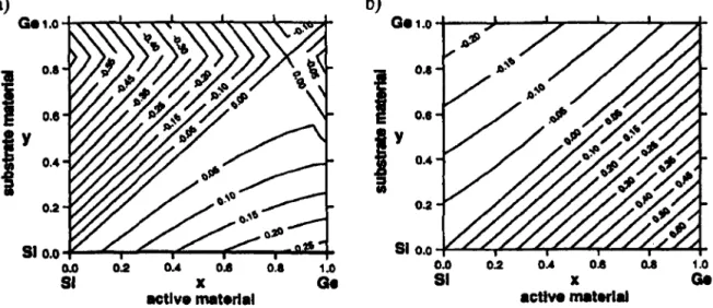
Figure 2.3 shows a complete set of contour plots for the offsets between the topmost valence bands (Ev'"OX(X)-Evmax(y» and the lowest conduction bands (Ecmill(x)_Ecmill(y» of a strained Sh-xGex layer on an unstrained Si1-yGey substrate based on empirical pseudopotential calculations of the valence and conduction bands [7].
a)
G.,.O -I-or-r""~"'C'""'I~T""'II::~T""'II::~~-m-::'"
0.2
51 0.0 -f'--..,...--,.---f---,~
...
0.081
0.2 0.. 0.8
x
actlv. meterlal0.'
1.0 Oeb)
i
0.1 0.'IY
0 ..i
0.2
51 0.0
0.0 0.2 0 .. 0.8
81
x
.cUve material
o.a 1.0 Ge
Figure 2.3 (a) Conduction-band offsets Ecmill(x)_Ecmill(y) and (b) valence-band offsets
The values were calculated using the defonnation potentials for the elements, as listed in Table 2.4, and linear interpolations for the alloys. Because of the approximations and interpolations involved, this approach is estimated to leave an uncertainty of the band offsets of about 100 meV. Only a limited number of experimental results conducted under well-defined strain conditions are available, mainly for Si/Ge, Si/Sil-xGex and Sh-xGex/Si heterostructures [5]. These basically confinn the respective theoretical offsets within the error margins mentioned.
Table 2.4 Defonnation potentials [7], spin-orbit splittings ~ and elastic constants ell and el2 for Si and Ge [2].
Si Ge
{~+{1I3)-Eu)L\-a (L\ minimum) 0.29 -1.90
{~+{l/3)-Eu)L-a (L minimum) -3.65 -5.17
a (eV) -10.2 -12.4
b{eV) 2.33 2.08
Eu L\ (L\ minimum) 9.29 10.20
~(meV) 44 296
en (l06 N·cm-2) 16.75 13.15
el2 (l06 N·cm-2) 6.5 4.94
There are four general features in Figure 2.3 worth mentioning. (i) The valence band maximum occurs always in the layer with the higher Ge content, independently of the strain condition. (ii) For x<y the conduction band minimum lies in the (tensilely) strained Sh-xGex layer, i.e. the band alignment in this regime is of type II. (iii) In an area defined by
x>y and y<0.6 the conduction band offset is smaller than ±20 meV, which means a basically flat conduction band alignment within the accuracy of the calculations. (iv) For Ge-rich strained layers (x>0.8) on Ge-rich substrates (y>0.6) a type-I alignment is predicted, i.e. the valence band maximum and the conduction band minimum are both located in the strained Sh-xGex layer. This prediction has yet to be confinned experimentally. Therefore Figure 2.3 allows predictions for arbitrary SiGe heterojunctions with respect to band offsets.
2.2.2
Strain adjustment in heterostructures
It has been shown in the preceding section that the valence and conduction band offsets in an Si/SiGe heterojunction depend strongly on the strain distribution throughout the layers, making strain as essential a parameter as the layer compositions. As has been detailed above, well-defined interface conditions require a conservation of the in-plane lattice constant, i.e. pseudomorphic (or coherent) growth of the active layers on a substrate whose lattice parameter has been properly adjusted. Hence, in order to exploit "strain engineering" for the tailoring of the band structure both the strain-defining substrate and the pseudomorphic heterolayers have to be realized. Bulk Sh-xGex can be ruled out as
substrates, both because of the inherent problems of pulling homogeneous Sit-xGex crystals, and because such substrates would jeopardize the main advantage of the Si/SiGe heterosystem, namely its compatibility with existing silicon technologies. It is therefore mandatory to employ Si substrates and provide strain adjustment by means of a relaxed, intermediate Sh-yGey buffer layer with the bulk lattice constant of the Sh-yGey. Occasionally, this combination is referred to as a virtual substrate (VS).
For relaxed buffers as well as for pseudomorphic layers the most relevant material parameter is the critical thickness te, an equilibrium parameter which is defined as the film
the actual growth environment. Low-temperature epitaxy techniques, such as molecular
beam epitaxy (MBE) or the different variants of low-temperature chemical vapour
deposition (CVD) can in this way significantly extend the range of useful layer
thicknesses. This is shown in Figure 2.4, where for Si1-xGex on Si substrate the equilibrium
critical thickness te and experimental values of films grown by MBE at 550C are plotted as
a function of x. Although reasonable film thicknesses appear feasible even at a higher
lattice mismatch, one has to keep in mind that metastable layers may partly relax upon
subsequent heat treatments.
The three phases labeled "stable", "metastable" and "relaxed" in Figure 2.4 mark the
limitations of strain engineering in the SiGe material system: strain within an active layer
is always associated with a maximum (critical) thickness of this layer. This usually
requires compromises concerning the maximum exploitable strain in such a layer, since
highly strained layers have necessarily to be so thin that quantum size effects finally limit
the achievable band offsets. On the other hand, relaxed buffer layers for strain adjustment
become relatively thick, since a high degree of relaxation and low defect densities are
required, which both rule out buffers deep in the metastable range.
I:lOO
,.
\ Sl, Ge on Si\
E
\
c ~
-
..J'\
\ relaxed
II) II) 100 (I,) c ~
"-.5:2 30 .c....
meta- " " MBE 550°C stable I ...a:I
<.>
10
E
....
'"
"
<.>
3
1
0 0.2 0.6 0.8
Ge concentration x
Figure 2.4 Critical thickness versus composition for Si1-xGex on Si. The lowest curve gives
the theoretical limit in thermal equilibrium [29], whereas the experimental curve is for a metastable layer grown at 550C by MBE.
Because of their importance for strain engineering, and the problems encountered in the initial attempts to realize such buffers, the next section will treat state-of-the-art buffer layer growth in some details.
2.2.3 Strain relaxed Sit_yGeylSi(OOl) buffer layers
The simplest way of implementing a strain-adjusting buffer layer is the growth of a constant-composition SiGe layer with a thickness exceeding te
*
by a large enough margin to allow a reasonably high degree of strain relaxation [31]. However, it was soon recognized that such buffer layers are associated with 109 to lOll threading dislocations per cm2 penetrating through the buffer, and ending at the respective growth front [32], [33]. A major reason for these unacceptably high densities lies in the step-like strain variation at the interface between the substrate and a constant composition buffer, which leads to an efficient confinement of the misfit dislocations to the (001) interface plane. For this orientation two equivalent networks of strain-relaxing misfit dislocations exist, which are defined by intersect of the [111] glide planes with the (001) interface plane, resulting inline vectors along the [110] and [1 TO] directions. Misfit accumulation in the interface plane causes substantial interactions between the two networks that can impede and even arrest the propagation of individual misfit dislocations. As a consequence, rather short misfit segments develop, which are associated with a high density of threading dislocations, because either end of a misfit segment has to be connected to a free surface via a threading dislocation.