A Battery Equalisation System for
Electric Vehicle
A thesis submitted in partial fulfillment
of the requirements for the degree of
Master of Engineering
at the
University of Canterbury
Christchurch, New Zealand
Department of
Electrical and Computer Engineering
By
i
Abstract
In 1999, the Electrical and Computer Engineering Department at the University of Canterbury started building their third electric vehicle (EV3) based on a TOYOTA MR2 with the goal of building a higher performance vehicle to match present combustion engined vehicles. The car is powered by 26 12volt sealed lead-acid batteries connected in series to achieve a nominal 312V DC source.
A battery voltage equaliser is a device that draws energy from a higher charged battery, then discharges into a lower charged battery. The need for a voltage equaliser is principally due to the differences in cell chemistry, temperature gradients along the battery string and the ages of the batteries. During the charging or discharging process, some batteries reach their nominal voltage or reach deep discharge states before the others. Then if the charger keeps charging the batteries or the load keeps drawing energy from these batteries, it results in damage to the batteries. Therefore maintaining the charge level on each battery becomes important. In addition, it also improves the battery life and vehicle travelling range.
This thesis details the analysis of three different types of battery equaliser, which are based on a 24W buck-boost converter, 192W buck-boost converter and 192W flyback converter. In this design, all converters are designed to work under current mode control with average of 2A. To make each converter install without significant effect on the performance and the cost, each converter is also built with the goals of being small, lightweight, cost effective, flexible for mounting, maintenance free and highly efficient.
ii
Acknowledgment
First and foremost, I would like to express my gratitude to my supervisors, Associate Professor Richard Duke and Dr. Simon Round for their advice, guidance, encouragement and being very patient throughout this project.
I would also like to thank all the members in the Power Electronics Research Group (William Chen, Si-Kuok Ting, Irene Ting, John and Ari) for giving me good advice and being as a good family in this research group. Special thanks to technician Ron Battersby, Ken Smart, Dudley Berry, Scott Lloyd and Nick Smith in the laboratory and sharing their practical experiences.
iii
Table of contents
Abstract………i
Acknowledgment………ii
Table of contents………iii
Table of Figures………v
Table of Tables………vii
Publication arising from this thesis………viii
1
Introduction………1
1.1. Project overview………1
1.2. Thesis structure………4
2
Battery Monitoring and Equaliser Topologies………6
2.1. Battery monitoring………7
2.2. Common bus topology………7
2.3. Common core topology………10
2.4. Ring topology………11
2.5. Selection of voltage equaliser configuration for EV3………13
3
Converter design………17
3.1. The 24W buck-boost converter………17
3.1.1. The PWM controller………18
3.1.2. Average current mode control………19
3.1.3. The gate drive………20
3.1.4. The power converter of the 24W buck-boost converter………21
3.2. The 192W buck-boost converter………31
3.3. The 192W flyback converter………32
3.3.1. PWM controller for the 192W flyback converter………33
3.3.2. 192W flyback transformer………34
3.3.3. Reducing the voltage stress on MOSFETs………37
iv
4
Converters simulations………40
4.1. 24W buck-boost converter………41
4.2. 192W buck-boost converter………43
4.3. 192W flyback converter………45
4.4. Summary………48
5
The system construction………49
5.1. The 24W Buck-boost converter………49
5.1.1. Inductor design………49
5.1.2. MOSFET selection………52
5.2. The 192W Buck-boost converter………54
5.3. The 192W Flyback converter………55
5.4. Summary………59
6
Performance records………57
6.1. Battery equalisation between non-isolated banks………59
6.2. Battery equalisation between isolated banks………63
6.3 Summary………58
7
Conclusion………70
Appendix ………73
The schematics of 24W buck-boost converter………74
The schematics of 192W buck-boost converter………75
The schematics of 192W flyback converter………76
The PCB of 24W buck-boost converter………77
The PCB of 192W buck-boost converter………78
The PCB of 192W flyback converter………79
The data sheet of E32 planar inductor………...80
The data sheet of E43 planar inductor ………81
The data sheet of SUD35N05-26L MOSFET………82
v
Table of Figures
Figure 1.1. Battery location………...2
Figure 2.1. The common bus equaliser………8
Figure 2.2. The common core equaliser………10
Figure 2.3. The ring equaliser………11
Figure 2.4. The proposed voltage equaliser structure……….13
Figure 2.5. The efficiency comparison of buck-boost and Cuk converters………14
Figure 2.6. The proposed voltage equaliser structure………15
Figure 3.1. The Buck-boost converter………17
Figure 3.2. The block diagram of SG3526………18
Figure 3.3. The average current mode control circuit………19
Figure 3.4. The RM core power rating curve.………23
Figure 3.5. 3C90 B-H curve………25
Figure 3.6. The construction of the planar inductor………27
Figure 3.7. The track width versus temperature rise diagram………28
Figure 3.8. The construction of the integrated inductor………29
Figure 3.9. The flyback converter………32
Figure 3.10. The PWM controller for the 192W flyback converter.………33
Figure 3.11 Flyback converter with clamping circuit………38
Figure 4.1. 24W non-isolated buck-boost converter………41
vi
Figure 4.3. 24W buck-boost converter equalisation.………43
Figure 4.4. 192W buck-boost converter………44
Figure 4.5. 192W buck-boost converter switching waveforms.………44
Figure 4.6. 192W buck-boost converter equalisation………45
Figure 4.7. The schematic of the 192W flyback converter………46
Figure 4.8. 192W flyback converter switching waveforms………46
Figure 4.9. 192W flyback converter equalisation.………47
Figure 5.1. RM, planar inductor and integrated inductors efficiency comparison……50
Figure 5.2. The inductor for the 24W buck-boost converter………52
Figure 5.3. The photo of the 24W Buck-boost battery equaliser………53
Figure 5.4. 24W buck-boost converter action waveforms………53
Figure 5.5. The 192W buck-boost converter………55
Figure 5.6. The frequency response curve of the 192W flyback converter.………56
Figure 5.7 The switching waveform with/without the clamping circuit………57
Figure 5.8 The photo of the 192W flyback converter………57
Figure 5.9. The switching waveform of the 192W flyback converter………58
Figure 6.1. The equalisation setup………60
Figure 6.2. Equalisation procedure………62
Figure 6.3. The setup diagram for non-isolated bank equalisation………63
Figure 6.4. Battery equalisation process for an eight series connected batteries………65
Figure 6.5. The setup diagram for isolated bank equalisation………66
vii
Table of Tables
Table 2.1. Comparison of equaliser topologies………...13
Table 4.1. The open-circuit voltages after 30A of 60 minutes discharge………40
Table 6.1. The measured battery open-circuit voltages………63
viii
Publication arising from this thesis
Chapter 1: Introduction
Page 1
1. Introduction
1.1. Project overview
The first electric car was invented by Thomas Davenport in 1834. At that time, the battery used in the car was not rechargeable. In the next few decades, numbers of electric cars and rechargeable battery technologies were developed, which brought more attention to investigate electric vehicle (EV) development. In the late 1890s EVs outsold gasoline cars ten to one. EVs dominated the roads and dealer showrooms. Some automobile companies, like Oldsmobile and Studebaker actually started out as successful EV companies, only later transitioning to gasoline-powered vehicles. In fact, the first car dealerships were exclusively for EVs[1].
Early production of EVs, like all cars, was accomplished by hand assembly. In 1910, volume production of gasoline powered cars was achieved with the motorised assembly line. This breakthrough manufacturing process killed off all but the most well-financed car builders. Independents, unable to buy components in volume died off. The infrastructure for electricity was almost non-existent outside of city boundaries, limiting EVs to city-only travel. Another contributing factor to the decline of EVs was the addition of an electric motor (called the starter) to gasoline powered cars, finally removing the need for the difficult and dangerous crank to start the engine. Due to these factors, by the end of World War I, production of electric cars stopped and EVs became niche vehicles, serving as taxis, trucks, delivery vans, and freight handlers[1].
Chapter 1: Introduction
Page 2
In the past thirty years, the University of Canterbury has also been investigating and developing its own EVs. The original EV was developed to test motor speed control ideas for AC induction motors.[2] In 1982, the second EV was developed, and that was based on a Austin Farina and powered by 20 series connected lead-acid batteries to form a nominal 240V dc bus. In 1999 the development of the third EV started with the goal of building a higher performance vehicle to match present combustion engined vehicles.
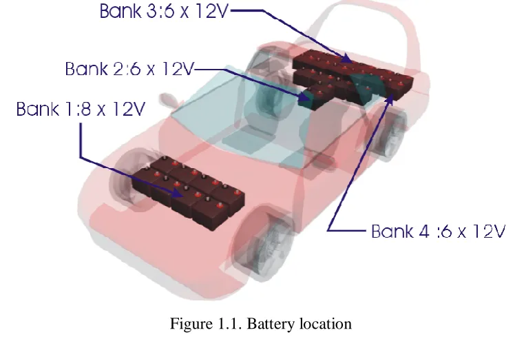
[image:12.595.94.468.448.694.2]The third electric vehicle (EV3) produced by the Electrical and Computer Engineering Department at the University of Canterbury is based on a TOYOTA MR2. It is powered by 26 Hawker Genesis 12volt 26A-hour sealed lead-acid batteries connected in series to achieve a nominal 312V DC source and these batteries are conveniently divided into four banks by the constraints of their location in the car. The first bank consists of 8 batteries, which are located under the front bonnet of the MR2. The second bank consists of 6 batteries and is placed in the engine bay at the back. The third and the fourth banks consist of 6 batteries each and are located in the rear boot. These battery locations are shown in Figure 1.1.
Chapter 1: Introduction
Page 3
Maintenance of cells at an equalised charge level is critical for enhancing battery life[1]. The need for a voltage equaliser is principally due to the differences in cell chemistry, temperature gradients along the battery string and the ages of the batteries. During the charging process, some batteries will consequently reach full charge before others and before the overall battery terminal voltage reaches its nominal value[1]. Therefore, if the charger continues to charge the remaining batteries, it would result in overheating the fully charged batteries, thus reducing their useful life. The same principle can also be applied to the discharging process. Any over-discharge would lead a battery into deep discharge, which can also reduce the life of the battery and decrease the travelling range of the electric vehicle.
The idea of a basic battery equaliser is to balance the charge level of two batteries by drawing energy from the one with the higher charge and transferring it to the other. To achieve this, a high frequency dc-dc converter is used. In power electronics, every converter has its own energy storage, which can be an inductor, a capacitor, a transformer or some combination of these. By controlling the switching signal, this energy storage capacity can be charged from the source and then discharged to the load. In a battery equaliser, the overcharged battery can be considered as the source and the undercharged battery as the load.
The objective of this thesis is to investigate various battery equalisation topologies that could be implemented into the EV3 to equalise the charge level of each individual battery within the entire battery string. Since there is a total of 26 batteries that need to be equalised, a number of equalisers have to be built for the entire battery string. Therefore, the design of each equaliser must be small, lightweight, cost effective, easy to interface, flexible for mounting, maintenance free and highly efficient.
Chapter 1: Introduction
Page 4
1.2. Thesis structure
In this thesis; various types of voltage equaliser topologies, which include the common core, common bus and ring equalisers are investigated. In Chapter two the principles of each equaliser topology are described. It demonstrates how the dc-dc converter can be used to interface between two batteries or two banks of batteries and then transfer the energy from one to the other. To design the most suitable equaliser for the EV3, the advantages and disadvantages of each topology, based on this construction, cost and future upgradeability are listed.
In Chapter three the design procedures of the dc-dc converters making up the equaliser are detailed. To minimise the converter size and to increase the manufacturability, various type of inductors, such as RM core, planar core and integrated inductor are also investigated. In this chapter, all electric specifications including the power rating, current ripple and the strategy of the control circuit of each converter are also defined.
In chapter four the simulations of all dc to dc converters making up the chosen equaliser topology are described. To achieve realistic results of simulations, discharging test measurements over eight series connected lead-acid batteries was first carried out. The result of these tests gives an indication of the possible voltage variations for each battery. The simulation is carried out by Pspice simulator and each rechargeable battery is modelled as a 1F capacitor. The simulation results demonstrate that the selected converters can be successfully used in the battery equalisation system.
Chapter 1: Introduction
Page 5
In Chapter six, two sets of equalisation results for the battery equalisation system are obtained. These equalisation tests are based on equalising two banks of four series connected batteries. Before each equalisation test, all batteries are equally charged to 13V. In the first equalisation test, the two banks are connected in series, which forms an eight series connected batteries string. Then the equalisation of individual batteries is done by seven buck-boost converters after the entire string battery has been discharged for an hour at a rate of 30A. After that, the 192W non-isolated buck-boost converter equalises the two banks of batteries to ensure each bank has an equal charge level. In the second equalisation test, the two banks of four series connected batteries are isolated from each other and the equalisation between each bank is done by an isolated flyback converter.
In Chapter seven, the conclusion finalises the overall design process and summarises the outcome. The difficulties and some considerations from the design of each converter are also described. In addition, some possible future investigations are also pointed out.
References:
[1] Electric Vehicle History. May 2005. Electric Auto Association (EAA), http://www.eaaev.org/Flyers/eaaflyer-evhistory.pdf
Chapter 2: Battery Monitoring and Equaliser topologies
Page 6
2. Battery Monitoring and Equaliser
Topologies
The idea of a battery equaliser is to balance the charge level of two or more batteries by drawing energy from the one with the higher charge and then discharging to a lower level battery. The most efficient means of achieving this transfer is by using a high frequency dc-dc converter. In power electronics, every converter has an energy storage, which may be an inductor, a capacitor, a transformer or some combination of these. By controlling the converter’s switching signal, this energy storage capacity is normally charged from the source then discharged to the load. In a battery equaliser the overcharged battery can be considered as the source and the undercharged battery as the load.
To design the most suitable voltage equaliser for the EV3, there are a number of concerns that have to be addressed. Due to the limited space in the car, the battery equaliser has to be compact. Further, since there are 26 lead-acid batteries in the car, a large number of battery equalisers are required in order to efficiently balance each individual battery. This makes the cost, construction, manufacturability and efficiency of the battery equaliser important aspects to consider.
The batteries used in the EV3 are rated at 26Ahr, and the equalisation rate is proportional to the operational current of the equalisation system. Unfortunately higher operational current brings larger power losses from the system, which results in increased switching losses. In order to achieve a reasonably fast equalisation rate and to minimise the power loss from the converter, the average operational current for this equalisation system is set to 2A.
Chapter 2: Battery Monitoring and Equaliser topologies
Page 7
2.1. Battery monitoring
The maintenance of cells at an equalised charge level is critical for enhancing battery life[1]. There are numbers of ways to monitor the charge level of a lead-acid battery, and the most common techniques are Coulometric measurement and open-circuit voltage measurement. Coulometric measurement counts the ampere-hours either coming out of or going into the battery bank. In its most basic form the battery capacity is assumed to be fixed, and then a sensor has to be used for every battery in order to determine how much energy has been drawn from or has flowed into the battery. In reality the total battery capacity varies with the discharge current, the type of discharge, temperature and the age of the battery[2]. Open-circuit voltage can be used to determine the state of charge and is more suited to battery monitoring in an electric vehicle, since the open-circuit voltage can be measured directly from standard battery terminals. The open-circuit voltage of a sealed lead-acid battery also relates directly to the battery’s state of charge[3]. The main drawback of the open circuit voltage monitoring technique is that the open-circuit voltage must stabilise before a reliable measurement can be made, and this can take from half an hour to several hours depending on the type of battery[3].
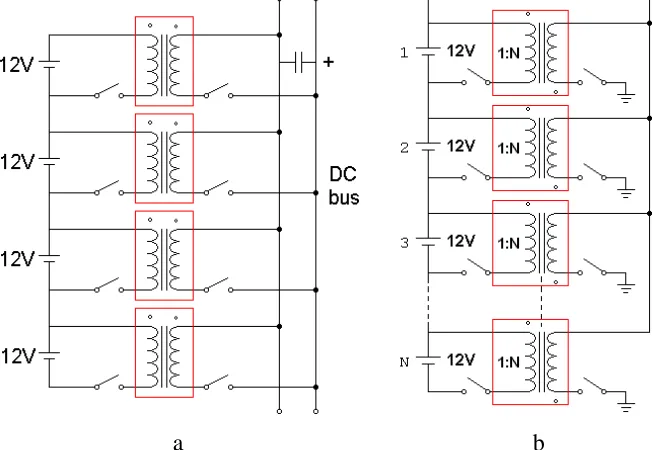
2.2. Common bus topology
Chapter 2: Battery Monitoring and Equaliser topologies
Page 8
[image:18.595.120.446.76.301.2]a b
Figure 2.1. The common bus equaliser
In the first common bus equaliser shown in Figure 2.1.a, the temporary energy storage is the common bus, which can be made up from a capacitor bank or a separate rechargeable battery. Energy transformation between any batteries in the series connected battery string is done by using the isolated converter to draw the energy from the higher charged battery, store the energy onto the common bus, and then using the other isolated converter to discharge this energy into the lower charged battery[1].
In the second common bus equaliser shown in Figure 2.1.b, there is no intermediate energy storage unit. When one battery is overcharged; the associated isolated converter will draw the energy from this overcharged battery, and then recharge the entire battery string [1]. On the other hand, if one battery is under-charged, the battery equalisation system would take the energy from the whole battery string to recharge the under-charged battery via its associated isolated converter.
Chapter 2: Battery Monitoring and Equaliser topologies
Page 9
Comparing these two common bus equalisers, the first common bus equaliser shown in Figure 2.1.a has the advantage of flexibility of the transformer ratio and is better for future expansion. Since the voltage rating on each side of the transformer is identical, the transformer ratio of the primary and secondary windings can be made as 1:1, which means the transformer ratio is not affected by the total number of the series string battery. So if any battery is required to be added to or removed from the electric vehicle, this common bus topology is very flexible for future expansion. However the major drawback of this common bus equaliser topology is due to the extra set of capacitors or battery used on the common bus side as the temporary energy storage, which brings an additional cost.
Chapter 2: Battery Monitoring and Equaliser topologies
Page 10
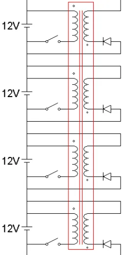
2.3. Common core topology
[image:20.595.220.345.331.591.2]The common core topology is shown in Figure 2.2. Compared with the common bus topology, the common core topology uses identical numbers of isolated dc-dc converters to equalise every battery. The difference is that in the common core topology all windings have to be coupled to the common core, which is the energy storage unit in this topology. The principle of this topology is that once the overcharged battery is detected; the converter will charge the common core by drawing the energy from the overcharged battery. Then distributing the stored energy in the common core to every battery along the series connected string battery via the diode, where the largest portion of the stored energy will be directed to the lowest voltage battery without any additional control [1].
Figure 2.2. The common core equaliser
Chapter 2: Battery Monitoring and Equaliser topologies
Page 11
core in order that all the secondary windings have identical inductance. In the EV3; the 26 batteries are divided into four banks and placed in three different compartments, which makes the common core topology difficult to implement. The other problem with this topology is that when dealing with large numbers of batteries in the string, a larger transformer core is required, which makes the equaliser difficult to mount, especially if space is a concern [1].
2.4. Ring topology
[image:21.595.225.400.390.519.2]The ring equaliser topology is shown in Figure 2.3. In this topology, the entire series string of batteries is considered as a ring. Within the string of batteries; every two adjacent batteries are linked by a non-isolated dc-dc converter and where the top and the bottom batteries are linked by an isolated converter to overcome the potential difference [1].
Figure 2.3. The ring equaliser
Chapter 2: Battery Monitoring and Equaliser topologies
Page 12
The non-isolated converters used in this topology could be either buck-boost or Cuk converters. In terms of manufacturability, the buck-boost converter has the advantage of a low component count, therefore the cost and the size of the converters can be kept to a minimum. By comparing the converter efficiency, due to the lower current ripple, the Cuk converter has higher efficiency than the buck-boost converter, which is important for high power transformation. To choose the most suitable non-isolating converter for the ring equaliser is dependent on how much power the converter needs to transfer. If the power rating is small, the extra power loss from the buck-boost converter could be negligible, and using fewer components could also reduce the manufacturing cost.
The isolated converter in this equaliser is used to provide electrical isolation and achieve energy transformation between the top and the bottom batteries of the string. Unlike the previous topologies, the ring topology only requires one isolated converter, and the turns ratio of the transformer is 1:1. This makes the isolated converter relatively easy to design, because this converter can work independently with no need to take the other converters into account.
Chapter 2: Battery Monitoring and Equaliser topologies
Page 13
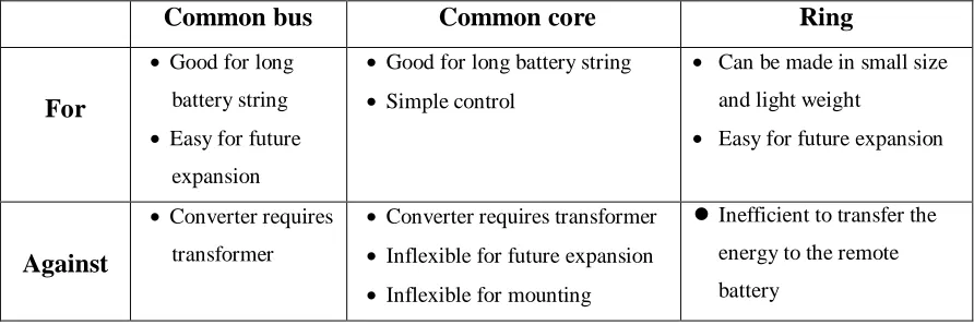
2.5. Selection of voltage equaliser configuration for EV3
A summarised comparison table of equaliser topologies is shown in Table 2.1.
Common bus Common core Ring
For
• Good for long battery string
• Easy for future expansion
• Good for long battery string
• Simple control
• Can be made in small size and light weight
• Easy for future expansion
Against
• Converter requires transformer
• Converter requires transformer
• Inflexible for future expansion
• Inflexible for mounting
[image:23.595.85.531.158.307.2]Inefficient to transfer the energy to the remote battery
Table 2.1. Comparison of equaliser topologies
[image:23.595.101.532.455.622.2]For the EV3 application, the ring structure is the most appropriate because most of the converters can satisfy the requirement of being small, non-isolated and easily manufacturable. In fact only one converter connected between the top and bottom of the battery string needs transformer isolation, and the proposed configuration is shown in Figure 2.4.
Figure 2.4. The proposed voltage equaliser structure
Chapter 2: Battery Monitoring and Equaliser topologies
Page 14
The key points for selecting the types of converters are the cost, manufacturability and efficiency. Unfortunately there is no single solution to satisfy all the requirements. For the non-isolated converters, the buck-boost configuration has the advantage of a low component count, therefore the buck-boost would have the advantages of high manufacturability and low cost. The Cuk converter has theoretically the highest efficiency when the converter is used for transferring energy between any adjacent batteries, but the drawback of the Cuk converter is if the converter is desired to have bi-directional energy transformation capability, the component count would be double that of the buck-boost converter. Therefore in order to decide which converter is the best choice, the converter efficiency comparison of the buck-boost and the Cuk converters was calculated through simulation. In this performance test both converters have a fixed input voltage of 12V, and by changing the input current, the efficiency of each converter over a range of power rating from 10W to 50W was measured. The results of these simulations are shown in Figure 2.5, which indicate there is no significant efficiency improvement when using the Cuk converter. Therefore the buck-boost converter was chosen as the non-isolated converter of the equaliser.
Buck-boost and Cuk converter efficiency comparison 88 90 92 94 96 98 100
10W 20W 30W 40W 50W
[image:24.595.148.417.428.584.2]Power rating E ff ic ie n c y ( % ) Buck-boost Cuk
Figure 2.5. The efficiency comparison of buck-boost and Cuk converters
Chapter 2: Battery Monitoring and Equaliser topologies
Page 15
transformation. However the price to pay for the single switch flyback converter is that the single switch flyback converter must dissipate the energy stored in the leakage inductance of the transformer in either the switch or a snubber associated with the switch. Other isolated converters with more than one switch such as the two switch flyback converter or half bridge forward converter perform better because the energy stored in the leakage inductance does not need to be dissipated.
The disadvantages of the isolated converter are the size, cost and the manufacturability of the transformer. For any converter that uses transformer as its energy transfer unit, if the operational voltage is low, the required minimum number of turns would be low, and the ratio of the primary leakage inductance to the primary inductance becomes too high, reducing the converter efficiency. Increasing the turns of the winding can solve this problem, but it would increase the size of the transformer and winding resistance.
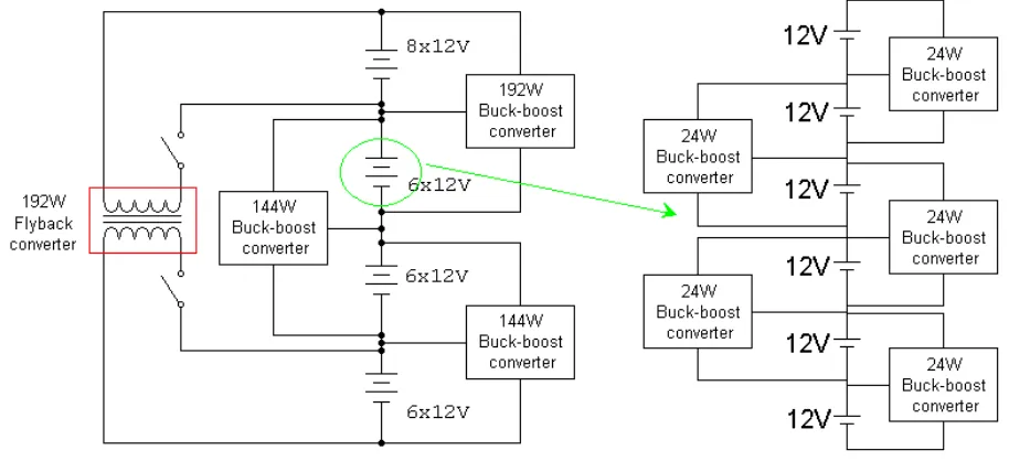
[image:25.595.91.548.509.718.2]The proposed ring voltage equaliser structure is shown in Figure 2.6. Within this structure, three 192/144W non-isolated buck-boost are used to balance the banks from the top to the bottom, and a isolated flyback converter is used to balance the energy between the top and the bottom bank. Inside each bank, the adjacent batteries are equalised by 24W non-isolated buck-boost converters. In this design, all the converters are designed for bi-directional energy transfer, with average currents selected as 2A, so that approximately 10% of total charge can be balanced in an hour.
Chapter 2: Battery Monitoring and Equaliser topologies
Page 16
In the next chapter, the design procedures of each converter are detailed. This includes the control strategy, and the design of each controller and converter. The calculations of each required component values are listed and several inductor core construction technologies are also introduced to achieve a more compact design.
References:
[1] PowerDesigner, “Dynamic Equalization Techniques For Series Battery Stacks” http://www.powerdesigners.com/InfoWeb/design_center/articles/NDCD/ndcd.shtm [2] Linden, D., Handbook of Batteries, 2nd ed. 1995, USA: McGraw-Hill.
Chapter 3: Converter design
Page 17
3. Converter design
In Chapter 2, the ring equaliser topology was chosen as the proposed equaliser structure for the EV3, and the primary reason for choosing this topology is that fewer isolated converters are required to make up a low profile, low cost and easily expandable voltage equalisation system. This battery equalisation system requires three different types of converter to be built, the 24W buck-boost converter, the 192W buck-boost converter and the 192W flyback converter.
In this chapter, the detailed design procedures of each converter are demonstrated, and the key factors of each converter are also discussed. The operational current for all converters are limited at 2A, and the target efficiency for all converters are 90%.
3.1. The 24W buck-boost converter
In the EV3, all 26 batteries are connected in series and divided into four banks. Within any bank, a 24W buck-boost converter is used to interconnect any two adjacent batteries. The design of this converter can be split into two parts: the controller and the power converter. The controller includes the PWM generator and the gate drive, which is used to drive the buck-boost power converter. The schematic diagram of the buck-boost converter for the 24W battery equaliser is shown in Figure 3.1.
Chapter 3: Converter design
Page 18 3.1.1. The PWM controller
The PWM controller is the heart of the converter. In this design, the two main functions that the controller provides are:
Generating the PWM switching signals to drive the power converter.
Sensing the pulse by pulse current signal from the converter, and converting this pulsed current signal into an average current signal, which is used to adjust the duty-cycle of the PWM signal to switch the MOSFETs.
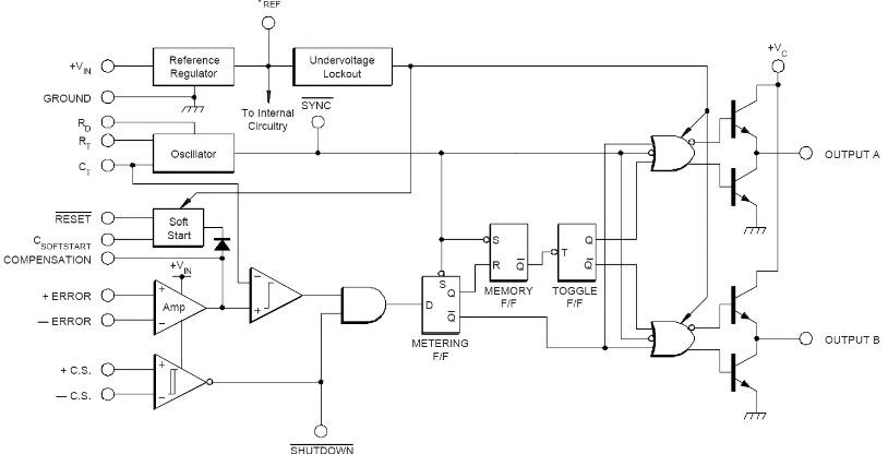
[image:28.595.81.488.532.740.2]The selected PWM control IC is SG3526 and its block diagram is shown in Figure 3.2. The SG3526 is a high performance monolithic pulse width modulator circuit designed for fixed-frequency switching regulators and other power control applications. Included in the 18-pin dual-in-line package are a temperature compensated voltage reference, sawtooth oscillator, error amplifier, pulse width modulator, and two low impedance power drivers. Also included are protective features such as soft-start and undervoltage lockout, digital current limiting, double pulse inhibit, a data latch for single pulse metering, adjustable deadtime, and provision for symmetry correction inputs. For ease of interface, all digital control ports are TTL and B-series CMOS compatible. Active LOW logic design allows wired-OR connections for maximum flexibility. This versatile device can be used to implement single-ended or push-pull switching regulators of either polarity, both transformerless and transformer coupled. The SG3526 is characterized for operation from 0°C to +125°C, and it is capable of generating PWM signals up to 350kHz with a duty cycle from 10 to 95%.[1]
Chapter 3: Converter design
Page 19
As mentioned in the previous chapter, the operational current of this battery equalisation system is set to 2A. To achieve this, all the PWM controllers will be designed to operate under average current mode control.
3.1.2. Average current mode control
The control strategy for the operation of any converter can be either voltage mode or current mode. In voltage mode, the output voltage of the converter is regulated. Therefore if the output impedance is high, the output current would be low, but if the load impedance is low, the output current would be high. Alternatively, with current mode control the output current from the converter is regulated, and the output voltage varies in response to load impedance changes. In this project, every converter was designed to transfer the energy at a constant rate of 2A; therefore, current mode control was employed.
A small shunt resistor or a current transformer are the common choices for current sensing. The shunt resistor is easier and cheaper to apply, but when a large current is involved, the shunt resistor generates larger conduction loss than the current transformer. In this design, since the regulated average current is only 2A, the shunt resistor has been chosen to sense the current signal.
Chapter 3: Converter design
Page 20
As shown in Figure 3.1, the current sensing resistor RCS is placed in series with the
inductor with neither end connected to ground. Therefore, a differential amplifier with a common mode range greater than 12V is required to accurately measure the current signal across RCS, and in this design the CA3140E op-amp was chosen, and the average current
mode control circuit is shown in Figure 3.3. This current mode control circuit can only measure one way of current flow. Therefore for this bi-directional battery equaliser, another set of this current mode control circuit is required.
Figure 3.3. The average current mode control circuit
This current mode control circuit can be divided into two parts. The first part is the differential amplifier, which is the current sensing part, and this is made up by CA3140E op-amp. The second part is the current limiting part, which is made up by the internal error amplifier of the SG3526 PWM controller. The operating principle of this current mode control circuit is first of all, the differential amplifier measures the signal from current sensing resistor. Then the 10nF capacitor will smooth the current signal, which makes it more like a dc voltage for the following current limiting circuit. In Figure 3.3, the 10kΩ potentiometer set the average operational current level, and in this application the average current is limited to 2A.
3.1.3. The gate drive
Chapter 3: Converter design
Page 21
The IR2112(S) is a high voltage, high speed, power MOSFET and IGBT driver with independent high and low side referenced output channels. Logic inputs are compatible with standard CMOS or LSTTL outputs, down to 3.3V logic. The output drivers feature a high pulse current buffer stage designed for minimum driver cross-conduction. Propagation delays are matched to simplify use in high frequency applications. The floating channel can be used to drive an N-channel power MOSFET or IGBT in the high side configuration, which can operate at up to 600 volts.[2]
3.1.4. The power converter of the 24W buck-boost converter
The design of the 24W buck-boost converter is characterised by two key components, the inductor and the MOSFET. The inductor is the energy storage unit in the buck-boost converter, and the MOSFET is the switching device of this converter. In the following section, the detailed inductor design procedure is listed, and to improve the manufacturability, the technology of the planar inductor and the integrated inductor are also investigated.
A - Inductor design on RM core
This inductor design procedure is carried out by the standard RM core, and the design consideration includes the core size, core material, required inductance and airgap. However, this design procedure can also be applied to other types of inductor cores.
Step 1: Select core material and core size
Chapter 3: Converter design
Page 22
Silicon steel is relatively inexpensive and easy to form. In addition, silicon steel is a metal with low resistivity. Low-core resistivity means silicon steel readily conducts electrical current. The result is that undesirable eddy currents can flow in the core material. Eddy currents contribute to heating and core loss. In addition, a silicon steel core tends to reach the point of saturation rather easily. When saturated, a core is unable to store additional magnetic energy. Rapid saturation results in reduced operating range[4].
Iron powder has higher resistivity than silicon steel. By special processing, iron particles are insulated from each other. The particles are mixed with a binder. The cores are then pressed into their final shape. Next, a baking process is used to cure the cores. After curing, many tiny air gaps combine to provide a distributed air gap effect, which also serves to insulate the particles from one another thereby reducing eddy current flow in the core. This extends the useful frequency range, but there is a trade-off. The binding material adds a distributed air gap to the core. The distributed air gap reduces the permeability of the core [4].
Ferrite is a crystalline magnetic material made of iron oxide and other elements. The mixture is processed at a high temperature and formed into a crystalline molecular structure. Unlike the other material, ferrites are ceramic materials with magnetic properties. Ferrites have high magnetic permeability and high electrical resistivity. Consequently, undesirable eddy currents are greatly reduced by ferrite cores. With their high resistivity, ferrites are ideal for use as inductors. For example, ferrite beads are frequently used to reduce parasitic oscillations and for general filtering at the component lead level. This type of broadband component requires a broadband low-Q in order to provide high impedance over a wide frequency range[4].
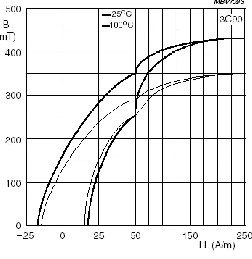
By comparing the characteristics of each core material, ferrite becomes the better choice for inductor design. However there are a numbers of different ferrite cores that can be chosen. Considering the cost, availability, the frequency and the flux density, the 3C90 material is selected.
Chapter 3: Converter design
Page 23
be mounted. Consequently, a core's geometrical shape can take the form of a cylinder, bobbin, toroid or several other complex shapes[4]. In the beginning of the inductor design the standard RM core is used to carry out the design process. Then the planar inductor and the integrated inductor technology will be demonstrated later on.
[image:33.595.145.481.304.607.2]The selection of the core size depends on the power that the converter is designed to deliver. If the core is too small, the inductor would be saturated during the operation. However there is harm to the converter efficiency when using a large inductor core, but choosing the right core size can reduce the manufacturing cost, size and the weight of the converter. The power rating to the core size curve is shown in Figure 3.4 [2], for this 24W buck-boost converter, the RM10 core is chose.
Figure 3.4. The RM core power rating curve.
Step 2, Calculating the minimum inductance.
Chapter 3: Converter design
Page 24
to higher conduction loss during operation. The standard terminal voltage of the battery is 12V, but when the battery is fully charged, the battery voltage can go up to 13V. Assuming the duty-cycle of the switching signal is 50%, if the converter operates at average current of 2A, the allowable peak current would be 8A in order to maintain the converter operates under continuous conduction.
However this assumption can only be made when the converter has 100% efficiency, but in reality it is not possible to achieve this. To make the design more practical, the maximum current ripple is set to 6A and the minimum inductance can be calculated by Equation 3.1.
I DT V L ∆ ⋅
= Equation 3.1
L = minimum inductance V = maximum input voltage D = duty-cycle
T = switching period
ΔI = allowable ripple current flow through the inductor
Assuming the maximum input voltage is 13V, switching frequency is 100kHz, 50% duty-cycle and 6A of ripple current. The minimum inductance is calculated as 11.9µH.
Step 3, Selecting maximum “on” period
Since the charge level of the battery is proportional to the terminal voltage of the battery, the input voltage of the converter will not stay at 13V at all times, as mentioned in the previous step. Therefore, in order to maintain the constant power flow when low input voltage occurs, the duty-cycle of the switching signal has to be increased, and the maximum “on” period is defined when the lowest input voltage occurs.
Chapter 3: Converter design
Page 25 Step 4: Calculating the air gap
For every dc to dc converter that uses an inductor, a sufficient air gap has to be carefully calculated. The air gap is used for storing energy from the dc source. An insufficient air gap would lead the inductor to saturate, which decreases the converter efficiency. Alternatively, if the air gap is too large, the inductance will be small, which leads the converter to operate in discontinuous conduction, which can also affect the converter efficiency. The air gap size can be calculated by Equation 3.2.
L A N e r ⋅ ⋅ ⋅ = 2 2 µ
α Equation 3.2
µr = 4π×10-7
N = number of turns Ae = area of the core, mm2 L = inductance, mH
From Step 1 and 2, the RM10 core was selected as the initial core size and the minimum inductance 11.9µH was also calculated. Assuming the number of turns N is equal to 10, the required air gap can be calculated as 0.507mm.
Step 5: Check core flux density and saturation margin
Chapter 3: Converter design
[image:36.595.161.408.79.333.2]Page 26
Figure 3.5. 3C90 B-H curve
The flux density consists of the ac flux density Bac and dc flux density Bdc. The sum of the ac and dc flux densities is the maximum flux density of the core, where the ac and dc flux density can be calculated by Equation 3.3 and 3.4.
e ac A N t V B ⋅ ⋅
= Equation 3.3
3 0
10 2 × −
⋅ ⋅ = ⋅ = α µ µ DC dc I N H
B Equation 3.4
V = Maximum supply voltage t = on time, µs
N = Number of turns Ae = Area of core, mm2 µ0 = 4π × 10-7
H/m IDC = Average DC current α = air gap, mm
Chapter 3: Converter design
Page 27
At the initial stage, if the maximum supply voltage V is set as 13Volts, the on time t = 5µs, number of turns N = 10, and the Ae is equal to 96 mm2. The Bac can be calculated as 67.7mT.
To calculate the Bdc, the number of turns N and the average current IDC were assumed as 10
and 2A. The air gap size α was calculated from Step 4, which is 0.5mm. Therefore the dc flux density is calculated as 25.1mT. The total flux density is equal to 92.8mT, which is well under the maximum allowable flux density of 350mT.
B - The planar inductor
Since 25 24W buck-boost converters need to be built and ideally located in a recess in the top of each battery, the manufacturing process for a low profile design has to be as simple as possible. The disadvantage of the conventional inductor is that it has a relatively large physical size. Therefore if 25 converters have to be installed into the EV3, they would occupy too much space and create a mounting problem. To overcome this mounting issue, the planar inductor and the integrated inductor technologies were investigated.
A planar inductor is constructed using either one E and one I core or two E cores, and the actual winding is made up by the loops of printed circuit board (pcb) tracks, where higher inductance can be achieved by multiple loops of a multilayer pcb. The biggest advantage of the use of the planar inductor is that since the windings are made up by the pcb tracks, the inductor can be made in a low profile, high precision and easily manufactured format. The constructions of the planar inductor are shown in Figure 3.5.
(a) (b) (c) (d)
Figure 3.6a. E core and I core
3.6.b. Fitting two multilayer pcb into the E core 3.6.c. Interconnecting the two pcb together
Chapter 3: Converter design
Page 28
[image:38.595.114.456.258.702.2]A major problem of the planar inductor is that if the pcb contains more than two layers, any intermediate windings would not have as much heat dissipating capacity as the top and bottom layers. Therefore, as the current flows through the winding, the pcb temperature will build up, then winding resistance and conducting losses will increase. To overcome this problem, a wider pcb track can be used to reduce the winding resistance and hence increase the current capacity and reduce the conduction losses from the inductor. The trade off by using the wider pcb track is the allowable numbers of turns per layer would be decreased. To emphasise the idea, Figure 3.6 shows how the pcb temperature can be varied by changing the track width.
Chapter 3: Converter design
Page 29 C – The Integrated Inductor
The integrated inductor is an inductor that has the form of an integrated circuit. Unlike the plastic package from the standard integrated circuit, the whole package of the integrated inductor is the inductor core, which has a built in air-gap. The leads of the package are the partial wirings of the inductor, and the inductor is completed by the pcb wiring. The construction of the integrated inductor is shown in Figure 3.7.
Figure 3.8. The construction of the integrated inductor
Compared with the standard inductor and the planar inductor, the integrated inductor has the advantages of the smallest physical size, and because there is no multi-layer pcb required, the pcb manufacture also becomes relatively simpler compared with the others. However, apart from these advantages, there are two disadvantages of this integrated inductor. The first drawback is due to this compact core size; the maximum inductance from a single integrated inductor can only be made around 5µH, which means the converter requires 250kHz or higher switching frequency. The second drawback is the cross section area of the pin out. The cross section area of the lead is 0.18mm2, which is eight times smaller than the litz wire that can be used on the RM core. The smaller cross section area brings higher dc resistance, which means the conduction loss from the inductor would be eight times higher.
D - MOSFET selection
Chapter 3: Converter design
Page 30
The voltage rating tells how much voltage MOSFET can handle between Drain and Source. For the buck-boost converters, the voltage between drain and source Vds would be equal to twice the supply voltage; therefore, the voltage rating of the MOSFET must be at least two times the supply voltage plus 20 percent of margin. Ideally the current rating is defined by the MOSFET peak operational current. However, in the converter design the pulse current also needs to be considered. Therefore, the continuous current and the pulse current determine that MOSFET rating.
The Rds-on is the on resistance when the MOSFET is in the on state. The low Rds-on
MOSFET has low conducting loss and in most cases is proportional to the voltage rating of the MOSFET. Therefore, it is not wise to select a high voltage rating MOSFET and operate it under low voltage conditions.
Ideally, higher switching frequency requires less inductance to maintain continuous conduction. Unfortunately, the high switching frequency means larger switching loss. The switching losses are created as a result of the simultaneous exposure of a MOSFET to high voltage and current during the transition between the open and closed states [3]. The fast transient requirement pushes us towards possibly high switching frequencies, which in turn increases the relative importance of the switching losses[3].
In reality it is difficult and uneconomical to manufacture and purchase the MOSFET, which has both low Rds-on and low switching loss. The low Rds-on MOSFET is normally made up of
a larger silicon area to reduce the on resistance, and the switching speed of MOSFETs is limited by the gate capacitance on the silicon, which is called the gate charge. The gate charge is the gate capacitance that needs to be charged or discharged during the on or off switching transition. The drawback of this larger silicon area is the creation of a larger gate capacitance. That makes the MOSFETs need more energy to be turned on, hence increasing the switching time and the switching loss. Therefore the compromise between the conducting loss and the switching loss has to be considered.
Chapter 3: Converter design
Page 31
for the required 24W buck-boost converters is 22. In each 24W buck-boost converter, each converter requires two MOSFETs, therefore the cost becomes a significant concern. In general, the price of the MOSFET is dominated by two factors; the voltage rating and Rds-on.
By allowing 20 percent allowance on both voltage and current signal, the voltage and current rating could be set to 29V and 2.4A. Then any MOSFET, which has a voltage rating higher than 29V and has a reasonably low Rds-on and price can be considered.
The gate charge defines whether the MOSFET has low switching loss or not. It determines the gate capacitance of the MOSFET, and it is mainly related to the Gate to Source voltage and is slightly affected by the Drain to Source voltage. In practice, the logic MOSFETs normally have lower gate charge because they only need 5V to be switched on instead of the 9 to 10V of the standard MOSFETs. Therefore by considering the factors of cost, conduction loss and switching loss, the logic MOSFET SUD35N05-26L is chosen for the 24W buck-boost converter and more details on this MOSFET will be discussed in chapter 5.
3.2. The 192W buck-boost converter
The 192W buck-boost converter is for transferring energy between the adjacent banks. The design procedure of the 192W buck-boost converter is similar to the previous 24W version, but there are three exceptional concerns that need to be considered. First, due to the input voltage is higher than the 24W buck-boost converter, so the selected MOSFETs should have higher voltage ratings. Second, since the power rating of this buck-boost converter is higher than the previous 24W version, a larger inductor core is required for storing larger energy. Third, assuming 90 percent efficiency is achieved, the total power loss from the converter would be 19.2W. Due to the majority of power loss being caused by the MOSFETs, heatsinks for each MOSFET are required in order to prevent overheating the MOSFET.
Chapter 3: Converter design
Page 32
the problem brought from choosing low gate charge MOSFETs and how to compromise between the low Rds-on or the low gate charge was also detailed. Then the result tells that
reducing the switching frequency is the better option to minimising the switching loss from the 192W buck-boost converter. In order to meet the electrical specification and minimising the cost, IRF740 is chosen for the 192W buck-boost converter.
The inductor design procedure is identical to the inductor design of the 24W buck-boost converter. However because the power rating of the converter has been increased, a larger inductor core is used. According to the RM core power rating curve from Figure 3.4, the minimum inductor core size for the 192W buck-boost converter would be RM14.
Alternatively the planar inductor core can also be used in this 192W buck-boost converter. According to the cross section area and the material, the E42 planar core would also be suitable for this application. However, due to the insufficient core size and the wiring space, the integrated inductor can not be used on this converter.
Reducing the switching frequency requires larger inductance to maintain the continuous conduction. By repeating the inductor design procedure in the design of the 24W buck-boost converter, if the switching frequency is reduced from 100kHz to 50kHz, and the duty-cycle and the allowable current ripple remain unchanged, the minimum inductance can be calculated as 192µH for the 192W buck-boost converter.
3.3. The 192W flyback converter
Chapter 3: Converter design
[image:43.595.136.492.67.289.2]Page 33
Figure 3.9. The flyback converter
This flyback converter is also designed for bi-directional energy transformation, and 2A of average operational current. In Figure 3.12, each side of the flyback transformer has its own PWM controller. Bank 1 represents the top bank and Bank 2 represents the bottom bank of the battery string; therefore, the reference voltage Vref_1 would be 216V higher than the Vref_2 because there are 18 batteries between these two reference points. The two Rcs are used for current sensing purposes, and the sensed current signal would be fed into Vcs, which is the current sensing input of the PWM controller. Then the PWM controller would adjust the duty-cycle to switch the MOSFETs.
3.3.1. PWM controller for the 192W flyback converter
Chapter 3: Converter design
Page 34
is used to sense the current signal and then the amplified current signal would be sent to the SG3526. The schematic of the flyback PWM controller is shown in Figure 3.9.
Figure 3.10. The PWM controller for the 192W flyback converter.
3.3.2. 192W flyback transformer
The key design of the flyback converter is the flyback transformer. The flyback transformer is used for storing and transferring energy from one side of the transformer to the other. Therefore, to design an appropriate flyback transformer becomes the most important factor of the flyback converter design. The construction of the flyback transformer can be seen as the combination of two inductors. Therefore, the inductor design procedure from the buck-boost converter is again used; moreover, the primary and secondary inductances can not be treated individually. Then some reiterative calculation would be required in order to make both primary and the secondary turns meet the electrical requirement, and the detailed transformer design procedure is shown below.
Step 1, Core selection
The core size depends on how much power the converter needs to deal with. From the design of the 192W buck-boost converter, the RM14 core was selected. According to the identical power rating, the RM14 core can also be used in this flyback transformer design.
Step 2, Calculating minimum primary inductance
Chapter 3: Converter design
Page 35
and the allowable current ripple are 13V and 6A. The minimum primary inductance can be calculated again from Equation 3.1, and the value of the minimum primary inductance is 174µH.
Step 3, Selecting maximum “on” period
In order to maintain the constant power flow, the maximum “on” period will occur at minimum input voltage and maximum load.[3] Assuming the input voltage is dropped to 11.5V, and the rest of the parameters from Step 2 remain unchanged, the maximum on period can be calculated as 57% from Equation 3.1.
Step 4, Select ac flux density swing
From Figure 3.4, the maximum allowable flux density is 350mT. The flux density swing also consists of both ac and dc flux densities, and from Figure 3.4, the ac flux density swing is initially selected as 250mT.
Step 5, calculate minimum primary turns
After the ac flux density is selected. By rearranging Equation 3.3, the minimum number of primary turns is shown in Equation 3.5, and according to the manufacture’s datasheet [4] of the RM14 core, the effective area of the centre leg is 198mm2.
e ac A B t V N ⋅ ∆ ⋅ =
min Equation 3.5
Nmin = minimum primary turns
V = applied dc voltage = 12 × 8 = 96V t = “on” times, µs = 10µs
∆Bac = maximum ac flux density, T. Assuming ∆Bac =250mT
Ae = minimum cross-section area of core, mm2. Ae = 198 mm2.
Therefore the minimum primary turns Nmin can be calculated as 20.
Step 6, Calculate secondary turns
Chapter 3: Converter design
Page 36
Primary volts per turn V/N = Vp/primary turns = 96/20 = 4.8 V/N
And then the secondary turn Ns = P P S V N V ⋅ Equation 3.6 = 96 20 72⋅ = 15
Where Vs = secondary voltage Ns = secondary turns
The secondary inductance can be calculated by Equation 3.7.
2
N Al
L= ⋅ Equation 3.7
L is the value of the inductance
Al is the equivalent quantity of the inductance N is the numbers of turn
Al is the equivalent quantity of the inductance in mH with a winding of 1000turns, which can be calculated from the primary turn and primary inductance, and the calculated Al is 3×10⁻⁷. Then the secondary was calculated as 67.5µH.
Step 7, Calculating the air gap size
The air gap calculation is very important in the flyback transformer design. An insufficient air gap would saturate the core, hence reduce the converter efficiency. Alternatively, if the air gap is too large, the inductance would become too small, which may lead to the inductor working under discontinuous conduction, and thus decrease the converter efficiency. The air gap can be calculated as 0.24mm from Equation 3.2.
Step 8, Check core flux density and saturation margin
The overall flux density of this flyback converter consists of the ac flux and the dc flux, and they can also be calculated by Equation 3.3 and 3.4. At this stage, the supply voltage V is made up by eight 12Volts batteries, which makes up a total voltage of 96 Volts. Assuming 50% duty-cycle, the on time t = 10µs, and from Step 4, the primary number of turns N is 20; and the effective area Ae of the E43 core is 198 mm2. Therefore, the ac flux density is
Chapter 3: Converter design
Page 37
To calculate the dc flux density, the number of turns N and the average current Idc were assumed as 20 and 2A. The air gap size α was also calculated as 0.23mm. Therefore the dc flux density is calculated as 109mT. The total flux density is equal to 349mT, which is under the maximum allowable flux density of 350mT.
In the buck-boost converter design, the planar core was introduced to improve the manufacturability. However, in the flyback converter design, due to the manufacturability, it is very difficult to make a pcb that has greater than four layers. Therefore, the planar core was not considered.
3.3.3. Reducing the voltage stress on MOSFETs
The voltage stress is the Drain voltage to overshoot during the turn-off edge, caused by the transformer leakage inductance.[3] Since the current flowing through the inductor can not be stopped instantaneously at the time that the MOSFET is switched off, the small amount of leakage inductance and this residual current would result in an overshoot across the drain and source of the MOSFET.
To overcome this effect, the voltage overshoot problem is best dealt with by ensuring that the leakage inductance is as small as possible, then clamping the tendency to overshoot by dissipative or energy recovery methods.[3] Minimising the leakage inductance can be made by shortening the wiring distance from the transformer to the other components. To achieve this, it is better to place the other components close to the transformer.
Chapter 3: Converter design
Page 38
Figure 3.11 Flyback converter with clamping circuit
In Figure 3.15, the flyback converter with the clamping circuit is displayed, and it shows each clamping circuit consists of three components, a diode Dc, a capacitor Cc and a resistor Rc. The diode is used to provide a current flow path for the energy stored in the leakage inductance. Therefore, when the MOSFET is turned off, the energy from the leakage inductance can flow into the clamping circuit. Then the Rc and Cc inside the clamping circuit would dissipate the energy from the leakage inductance.
There is no rule for selecting the value of the Rc and Cc. The values of Rc and Cc depend on how fast the energy from the leakage inductance needs to be dissipated. If the RC time constant is large, less voltage stress appears on the MOSFET. However, the drawback of the clamping circuit is that during the off state the voltage across the MOSFET is equal to the sum of the input voltage and the voltage across the flyback transformer. Therefore, if large clamping resistance and capacitance are used, the clamping circuit would require more time to charge the clamping capacitor Cc, which increases the MOSFET turn off time, hence increases the switching loss.
Chapter 3: Converter design
Page 39 3.4. Summary
In this chapter, the design procedures of three different converters - 24W buck-boost, 192W buck-boost and 192W flyback converters were detailed. The PWM controllers for all three types of converters are very similar. However there are two exceptional design considerations. First, as there is only one switching device on the 192W flyback converter and the MOSFET is connected to the reference point via the current sensing resistor. Therefore, there is no high-side drive required for this converter. Second, unlike the buck-boost converter, the current sensing resistor of the flyback converter is not sitting on the voltage source like the buck-boost converter does. So the additional op-amp for providing wide common mode range is not needed.
In the next chapter, the simulations of each converter will be made by Pspice simulator. The component values calculated in this chapter are also applied into these simulation tests. The simulation results include the detailed equalisation process and the switching waveforms on each key component, and finally it shows the energy between the two batteries can be successfully balanced by the designed converter.
References:
[1] Data sheet of SG3526
[2] Philips inductor core material
[3] Keith Billings, “Switchmode power supply handbook second edition”, 1999
Chapter 4: The simulations
Page 40
4. Converters Simulations
In this Chapter the results from the simulations of each converter making up the chosen voltage equaliser topology are discussed. The simulation models include one 24W non-isolated buck-boost converter, one 192W non-non-isolated buck-boost converter and one 192W isolated flyback converter. The simulations were carried out by Pspice simulator and in these simulations two rechargeable batteries or banks of batteries were modelled as two 1F capacitors, and the battery internal resistance and the wiring resistances were modelled as two 100mΩ resistors.
Before the simulation, a series connected battery discharging test at a rate of 30A for 60 minutes through a resistive load was done in order to measure what the nominal voltages from each battery would be after the batteries have been discharged. In the EV3 there are 26 batteries connected in series. Drawing energy from each battery at a rate of 30A is equal to drawing 10kW of energy, which is roughly equal to the power consumption of standard city driving. In this battery discharging test, eight sealed lead-acid batteries were first parallel connected and equally charged, and then connected in series, and the discharging result is shown in Table 4.1.
Batt 1 Batt 2 Batt 3 Batt 4 Batt 5 Batt 6 Batt 7 Batt 8 Average voltage Starting
voltage 12.62 12.78 12.74 12.76 12.65 12.72 12.71 12.76 12.72 End voltage 11.34 11.64 11.5 11.5 10.87 10.76 10.88 11.72 11.28
Difference from the average end
voltage
+0.06 +0.36 +0.22 +0.22 -0.41 -0.52 -0.40 +0.44
Table 4.1. The open-circuit voltages of each battery after 30A of 60 minutes discharge
Chapter 4: The simulations
Page 41
following simulations, the initial voltage of the source and the target batteries will have 1 volt difference.
4.1. 24W buck-boost converter
The voltage equaliser based on the 24W non-isolated buck-boost converter is shown in Figure 4.1. In this configuration, C1 represents the higher voltage battery and C2 is the battery required to be recharged, and the initial voltage these batteries are set to 12.5V and 11.5V respectively. In this simulation, the switching frequency was set to 100kHz, the inductor wiring resistance R3 is 15mΩ and the inductance value is set to 18µH, which is the minimum inductance value to maintain continuous conduction.
Figure 4.1. 24W non-isolated buck-boost converter
The aim of this simulation is to transfer the energy from C1 to C2, and the detailed switching waveforms of the MOSFET and the inductor are shown in Figure 4.2. In these simulation results, the PWM switching signal is represented by the switching signal V1. Vds indicates the drain to source voltage of Q1. IC1 and IC2 show the current flow from the
source and target batteries C1 and C2. Finally, IL represents the current flow through the
Chapter 4: The simulations
Page 42
[image:52.595.64.506.184.514.2]When the PWM switching signal V1 of this equaliser is high, Q1 turns on, then inductor L is charged by C1 via R1 and Q1. Later when V1 is switched low, Q1 turns off, the current stops flowing from C1, the inductor current keeps circulating and the stored energy in the inductor is discharged into C2 through R2 and the internal diode of Q2 without any additional control.
Figure 4.2. The switching waveforms of the 24W buck-boast converter.
Chapter 4: The simulations
Page 43