warwick.ac.uk/lib-publications
Original citation:
Suzuki , Takayuki, Lawrence, James, Walker, Marc, Morbec, J. M., Blowey, Phil J., Yagyu, K., Kratzer, P. and Costantini, Giovanni. (2017) Indium coverage of the Si(111)- 7×3 -in surface. Physical Review B (Condensed Matter and Materials Physics), 96 (3). 035412.
Permanent WRAP URL:
http://wrap.warwick.ac.uk/93951
Copyright and reuse:
The Warwick Research Archive Portal (WRAP) makes this work by researchers of the University of Warwick available open access under the following conditions. Copyright © and all moral rights to the version of the paper presented here belong to the individual author(s) and/or other copyright owners. To the extent reasonable and practicable the material made available in WRAP has been checked for eligibility before being made available.
Copies of full items can be used for personal research or study, educational, or not-for-profit purposes without prior permission or charge. Provided that the authors, title and full bibliographic details are credited, a hyperlink and/or URL is given for the original metadata page and the content is not changed in any way.
Publisher statement:
© 2017 American Physical Society A note on versions:
The version presented here may differ from the published version or, version of record, if you wish to cite this item you are advised to consult the publisher’s version. Please see the ‘permanent WRAP URL’ above for details on accessing the published version and note that access may require a subscription.
Indium coverage of the Si(111)-
√7 ×√3-In surface
T. Suzuki,1,2J. Lawrence,2M. Walker,3J. M. Morbec,4P. Blowey,3,5K. Yagyu,1P. Kratzer,4G. Costantini2
1Department of Electronics Engineering and Computer Science, Fukuoka University,
Fukuoka 814-0180, Japan
2Department of Chemistry, University of Warwick, Coventry, CV4 7AL, United Kingdom
3Department of Physics, University of Warwick, Coventry, CV4 7AL, United Kingdom
4Faculty of Physics, University of Duisburg-Essen, Lotharstrasse 1, 47057 Duisburg,
Germany
5Diamond Light Source, Harwell Science and Innovation Campus, Didcot, OX11 0QX,
UK.
Abstract
The Indium coverage of the Si(111)-√7 ×√3-In surface is investigated by means of X-ray photoelectron spectroscopy and first-principles density functional theory calculations. Both experimental and theoretical results indicate that the In coverage is rather a double layer than a single layer. Moreover, the atomic structure of the
Si(111)-√7 ×√3-In surface is discussed by comparing experimental with simulated scanning tunneling microscopy (STM) images and scanning tunneling spectra with the calculated density of states. Our structural assignment agrees with previous studies except for the interpretation of experimental STM images.
Introduction
Indium deposition on a Si(111) substrate in ultra-high vacuum (UHV) conditions has been already investigated extensively, and reported to show various reconstructions, such as √3 ×√3, √31 ×√31, 4×1, 2×2, √7 ×√3, depending on the In coverage and subsequent annealing temperature [1-3]. However, the atomic structures of these reconstructions are generally not yet well established, except for the√3 ×√3and the 4×1 reconstructions. The former has 1/3 monolayer (ML, defined with respect to the as-cut Si(111)-1×1 surface and corresponding to 7.83 atoms/nm2) coverage with one In adatom adsorbed on each T4site, while the latter has 1 ML coverage with rows of In atoms in an
approximately close-packed arrangement along the [110] direction [4-6]. The 4×1 reconstruction is also reported to undergo a surface structural phase transition from 4×1 to 8×2 below 100-130 K, due to the formation of a charge density wave [7-11].
Among these reconstructions, the√7 ×√3has attracted much interest recently, because it shows a free-electron-like two dimensional metallic state [12,13] and superconductivity at about 3 K [14-18]. It is reported that two phases of the√7 ×√3 reconstruction exist, which show slightly different appearances in scanning tunneling microscopy (STM) images, from which they derive their names: a hexagonal and a
“hex” and “rect” phases in several literature reports [19-24].
In the present study, we have investigated the In coverage on the √7 ×√3 reconstruction by X-ray photoelectron spectroscopy (XPS) and first-principles density functional theory (DFT) calculations. Moreover, we have discussed its atomic structure by comparing experimental STM images and scanning tunneling spectroscopy (STS) curves with simulated STM images and calculated density of states (DOS). Our results clearly indicate a coverage of 2.4 ML (double layer) for the Si(111)-√7 ×√3-In reconstruction, with “rect” being the most stable phase.
Experimental
The Si samples used in the present study were cut out from an-type
phosphorus-doped Si(111) wafer (0.007-0.013 Ω cm, Siltronix). They were ultrasonically cleaned in
pure acetone, ethanol and deionized water, and then introduced immediately into the UHV chamber of either the XPS or the STM instrument. After being outgassed at 500 ºC for several hours, the Si samples were flashed to 1200-1250 ºC several times, in order to obtain the clean 7×7 reconstruction. Indium (shot, 1-3 mm, 99.9999 %, Matek) was fixed by melting onto a tungsten filament and then sublimed by heating the tungsten filament by direct current, onto substrates held at room temperature (RT).
The XPS data were collected using an Omicron Multi-probe with the Si sample
being illuminated using an XM1000 monochromatic Al kα x-ray source (Omicron
Nanotechnology) at the Warwick Photoelectron Facility, University of Warwick. Its base pressure is about 2 × 10⁻¹⁰and 2 × 10⁻¹¹mbar for the preparation and the XPS chambers, respectively. The core levels were recorded using a pass energy of 10 eV (resolution approx. 0.47 eV). Measurements were made at room temperature and at a take-off angle of 90º with respect to the surface parallel. Low energy electron diffraction (LEED) patterns were recorded each time either before or after the XPS measurement, in order to confirm the surface structure. The XPS data were analyzed using the CasaXPS package [25] and the COMPRO package [26] employing Shirley backgrounds.
The STM images were taken using a commercial low-temperature STM system operated in UHV at the University of Warwick. Its base pressure is about 1.5 × 10⁻¹⁰mbar. The images were acquired in constant current mode at a temperature of 77 K using chemically etched tungsten tips. The Gwyddion software was used to process the STM images [27]. dI/dV spectroscopy was performed by adding a sinusoidal modulation voltage to the bias voltage via an internal lock-in amplifier and recording the output of the lock-in tuned on the first harmonic. Typical parameters for the acquisition of the spectra were: stabilization current I = ~0.5 nA, stabilization bias voltage V = +1.6 V, frequency f and amplitude A of modulation for the lock-in amplifier: f = 3.1 KHz, A = 10 mV. The spectra consisted of 400 sampling points, uniformly spaced between +1.6V and –1.6V.
Computational methods
density-functional theory [28] as implemented in the FHI-aims code [29], an all-electron full-potential code with numeric atom-centered basis functions. We used the generalized gradient approximation (GGA) proposed by Perdew, Burke, and Ernzerhof (PBE) [30] for the exchange-correlation functional and “tight” settings from the FHI-aims code with “tier2”, “tier3” and “tier2” basis sets for In, Si, and H, respectively. Convergence criteria of 10−5electrons/Å3and 10−6eV were applied for the charge density and the total energy, respectively.
The Si(111)-√7 ×√3-In surface was modeled within the supercell approach with five Si bilayers and a vacuum region of about 30 Å. Hydrogen atoms were used to passivate the rear side of the slab while the In atoms were adsorbed on the front side of the slab. We used the calculated bulk lattice constant of silicon, 5.47 Å, for the lateral dimensions of the unit cell. In the structural relaxations, the bottom Si bilayer was constrained to the bulk position whereas the remaining four Si bilayers as well as the In atoms were allowed to relax; we considered a convergence criterion of 5 × 10⁻³eV/Å for the maximum residual force component per atom. The Brillouin zone was sampled on a 8×12×1 Monkhorst-Pack [31] k-point grid. The STM images were simulated using the Tersoff-Hamann approach [32] where the tunneling current is assumed to be proportional to the local density of states (LDOS) of the surface at the position of the STM tip integrated over an energy interval above or below the Fermi level (for empty state or filled state images, respectively). In order to model the experimental acquisition of STM images in constant current mode, we use a constant density (in the range of 10-3to 10-5 electrons/ Å-3) and plot the height above the surface where the integrated LDOS equals this density.
Results
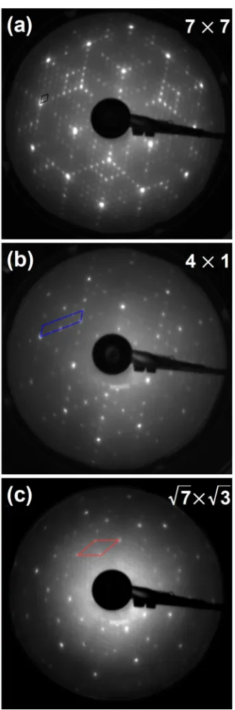
Figure 1 shows typical LEED patterns of the clean 7×7, the 4×1 and the√7 ×√3 reconstructions. Black, blue and red parallelograms in the figure show reciprocal unit cells of these reconstructions. As the Si(111) surface has three-fold rotational symmetry, the LEED patterns of the 4×1 and the√7 ×√3show a mixture of the three domains rotated with respect to each other by 120º. For preparing the Si(111)-√7 ×√3-In surface, sufficient Indium was deposited onto the clean Si(111)-7×7 substrate, followed by a short surface heating for 1-10 s up to 500 ºC. By this short heating, excess In atoms were desorbed from the sample surface, and its reconstruction changed to the√7 ×√3. Longer heating for 10-12 min at 500 ºC induced further desorption of In atoms, and the surface reconstruction changed to 4×1. Prior to the XPS experiments, In deposition times of 10, 12.5 and 15 min with a short heating were checked in the LEED, and found to have caused the 4×1, ‘a mixture of the 4×1 and the √7 ×√3’ and the √7 ×√3 reconstructions, respectively. Therefore, we deposited Indium for 15-18 min in the following XPS experiments in order to minimize the amount of Indium deposited, and to avoid overestimation of the In coverage, although excess In atoms were desorbed from the sample surface by a short heating at 500 ºC after the In deposition.
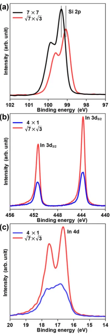
The experimental procedure is as follows. First, the√7 ×√3reconstruction was prepared in the preparation chamber of the XPS instrument, which was confirmed by the LEED pattern. Then, the sample was transferred to the XPS chamber, and a first XPS spectrum (red curve) was recorded. After that, the sample was flashed to 1250 ºC (to recover the clean 7×7 reconstruction) without moving it, in order to avoid any change in the experimental photoemission setup. A second XPS spectrum (black curve) was recorded and the sample was then transferred back to the preparation chamber, in order to confirm the 7×7 reconstruction by LEED. The Si 2p3/2(large, lower binding energy, BE) and Si
2p1/2(small, higher BE) peaks are resolved in both black and red spectra. The thickness
of the deposited In layer on the√7 ×√3is estimated to be 0.58 nm (= 2.3 ML) from the attenuation of the Si 2p intensity (sum of the 2p3/2and 2p1/2components) evident in Fig.
2(a) (see Supplemental Material [33]). Therefore, the In coverage is closer to a double layer (2.4 ML) than to a single layer (1.2 ML). The main peak of Si 2p3/2at 99.29 eV on
the 7×7 was shifted to 99.05 eV on the√7 ×√3, as indicated by the two thin lines. This is attributed to band bending induced by charge transfer between the In layer and the Si substrate, although the amount of the shift of 0.24 eV is smaller than the previously reported values of 0.44 eV [34] and about 0.6 eV [35]. These differences are most probably due to the differences in the doping of the Si substrates.
A similar sample transfer procedure was employed to acquire the blue and the red spectra in Figs. 2(b) and 2(c), which were recorded at the same position on the sample surface on the 4×1 and the√7 ×√3reconstructions, respectively. In between the first (red curve) and the second (blue curve) XPS measurement, the sample was heated for 10-12 min at 500 ºC in order to change the reconstruction from√7 ×√3to 4×1 – which was successively confirmed by LEED – without altering the experimental photoemission setup. The ratio of the In 3d5/2 intensities in Fig. 2(b) for the √7 ×√3 and the 4×1
reconstructions is about 2.0, and that of the In 4d intensity (sum of the 4d5/2 and 4d3/2
components, not resolved for the blue curve) in Fig. 2(c) is about 2.1. This corresponds to an In coverage of 2.0 ML and 2.1 ML, respectively, assuming an In coverage of exactly 1.0 ML for the 4×1 reconstruction. Moreover, the absolute In coverages for the√7 ×√3 and the 4×1 reconstructions were also estimated from the ratio of the Si 2p and the In 3d5/2 intensities via the thickogram method [36], resulting in values of 2.3 ML and 1.0
ML, respectively. In summary, all our evaluations based on the analysis of the XPS peak intensities indicate a double layer rather than a single layer In coverage for the
Si(111)-√7 ×√3-In surface.
Figure 3(a) shows a typical STM image of the√7 ×√3surface prepared in the STM instrument. Because of the three-fold rotational symmetry of the Si(111) surface, three domains are seen on the terrace as indicated by three dotted lines in the right-hand side of the figure, agreeing with the LEED pattern in Fig. 1(c). Enlarged filled and empty state STM images of the surface are shown in Figs. 3(b) and 3(c), respectively, where one unit cell is marked by a red rectangle in Fig. 3(b). We repeated the preparation of the
√7 ×√3reconstruction many times and the measured STM images, at the given sample bias voltage (Vs) and tunneling current (I), were always similar to those shown in Fig. 3.
for energetic reasons (see below), and the two different STM images reported in Figs. 2(b) and 2(c) of Ref. [24] and in Fig. 6 of Ref. [2] are likely to correspond to the “rect” phase with 2.4 ML coverage, which shows a different appearance depending on the bias voltage and the tunneling current. In fact, in our STM image simulations within the Tersoff-Hamann approach, we obtained STM images for the “rect” phase similar to both Figs. 2(b) and 2(c) of Ref. [24] by varying the bias voltage and the charge density. We were unable, however, to obtain a simulated STM image for the “hex” phase similar to the Fig. 2(b) of Ref. [24](see Figs. S2 and S3 in the Supplemental Material [33]).
A STS spectrum taken on the√7 ×√3reconstruction is shown in Fig. 3(d). There is one peak at about –0.8 eV in the filled state region and another small peak at about +0.9 eV in the empty state region, which qualitatively agrees with the previous STS result shown in Fig. 6 of Ref. [19]. As I-V and dI/dV curves in Fig. S1 in the Supplemental Material [33] show a finite differential conductivity at the Fermi energy (= 0 V), there is no band gap, indicating that the√7 ×√3is electronically metallic, in agreement with previous reports [12,13].
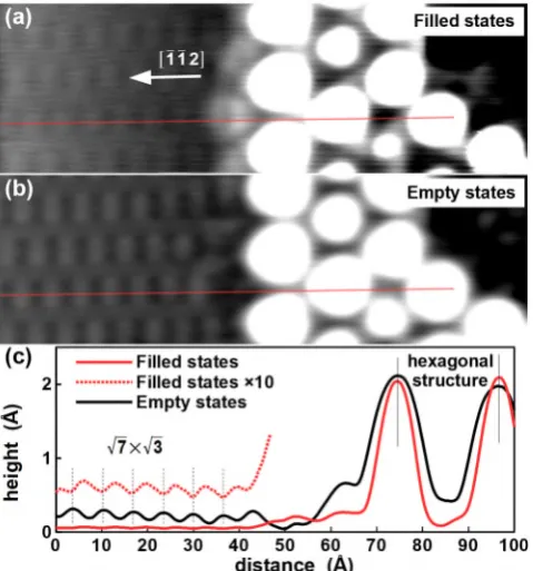
Figures 4(a) and 4(b) show filled and empty state STM images taken at the same sample position. The left hand side of the images corresponds to the √7 ×√3 reconstruction, while the right hand side shows a hexagonal structure (not the “hex” phase!) formed incidentally on the√7 ×√3,which was reported also in Ref.[37]. Figure 4(c) displays two line profiles measured along the red lines in Figs. 4(a) and 4(b). The peaks of the hexagonal structure (right hand side in Fig. 4(c)) can be used to calibrate the relative positions of the line profiles, demonstrating that the contrast of the√7 ×√3 reconstruction is reversed between filled and empty state STM imaging along the[1¯1¯2] direction.
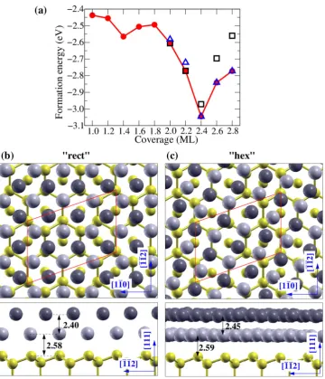
First-principles calculations were performed to determine the ideal coverage of In on Si(111)-√7 ×√3. The formation energies as a function of the In coverage are shown in Fig. 5(a); we defined the formation energy, , as = ( ) − ( )− ⋅ In,
where ( ) and ( )are the total energies of the Si(111)-√7 ×√3-In and
Si(111)-√7 ×√3surfaces, respectively, Inis the energy of the bulk In and is the number of In atoms in the system. The deep minimum at 2.4 ML observed in Fig. 5(a) clearly indicates a double-layer coverage of 2.4 ML In atoms (with six In atoms per unit cell in each layer), in agreement with the experimental findings discussed in the previous paragraphs and with a recent first-principles study by Park and Kang[38]. Although we found a shallow local minimum at 1.4 ML (which was also reported in Ref.[38]), different coverages of In on Si(111)-√7 ×√3are unlikely to form. For coverages higher than 1.8 ML we can identify the “rect” and the “hex” models proposed in Ref. [23]; their formation energies are indicated in Fig. 5(a) by blue triangles and black squares, respectively. For 2.4 ML we found that “rect” is the most stable configuration with formation energy ~74 meV per unit cell lower than the “hex” phase. Our result agrees with a previous first-principles study by Park and Kang [23], which predicted that the “rect” model is 0.05 eV more stable than the “hex” one. This indicates that In on Si(111)-√7 ×√3forms a double layer structure with 2.4 ML coverage, and only the “rect” phase exists.
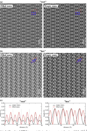
almost rectangular lattice; the lateral sizes of the rectangles ranging from 3.22 to 3.43 Å for the bottom In layer and from 3.18 to 3.47 Å for the top In layer. In atoms in the top layer are located at the center of the rectangles of the bottom layer, at a relative height of about 2.40 Å with respect to the bottom layer. In the “hex” phase the In adatoms are arranged on an oblique lattice with lateral sizes between 3.07 and 3.58 Å for the bottom layer and between 3.15 and 3.60 Å for the top layer; the center of mass of the top layer is about 2.45 Å above the bottom layer. We notice that the interatomic distances in the “rect” phase are closer to the lattice parameters of bulk indium (a=3.31 Å and c/2=2.49 Å for the body-centered tetragonal lattice, computed using the PBE functional) than those of the “hex” phase, which might explain why the “rect” phase is the most stable one at 2.4 ML of In and above.
Our computed interlayer distances (see Figs. 5(b) and 5(c)) between the In-In (2.40 Å for “rect” and 2.45 Å for “hex”) and In-Si layers (2.58 Å for “rect” and 2.59 Å for “hex”) are in close agreement with the values reported by Park and Kang [23], namely 2.42/2.60 Å for “rect” and 2.47/2.61 Å for “hex”. We found, however, a significant difference in height of the top-layer In atoms in the “hex” phase when compared to the “rect” phase: while in the “rect” configuration the heights of the top-layer In atoms differ from each other by less than 0.05 Å, in the “hex” configuration the difference in height ranges from 0.05 to 0.20 Å. The difference in height of the top-layers In atoms in the “hex” phase is also reflected in the simulated STM images displayed in Fig. 6. We further notice that, in particular in the empty state image (right panel in Fig. 6(b)), not all the six top-layer In atoms are visible in the simulated STM image. This was also discussed by Park and Kang in Ref. [23], who reported to see five (and not six) protrusions in the STM image of the “hex” phase. They additionally computed the charge corrugation for the “hex” configuration, obtaining a value of 0.23 Å for the maximum height difference between the peaks [23]; this result is consistent with the difference in heights between the top-layer In atoms observed in our calculations (between 0.05 and 0.20 Å).
The simulated STM images of the “rect” phase (Fig. 6(a)) show, for both filled and empty states, pronounced features along the [1¯1¯2] direction, as observed in the experimental STM images (Figs. 3(b) and 3(c)). These features correspond to In-In bonding states. In the “hex” configuration (Fig. 6(b)), on the other hand, a row of bright spots can be seen along the[3¯21]direction. We notice that the experimental STM images in Figs. 3(b) and 3(c) agree better with the simulated STM images of the “rect” phase in Fig. 6(a) than with those of the “hex” phase in Fig. 6(b). Our simulated STM image for the “rect” phase also compares well with the STM images displayed in Fig. 2(b) of Ref. [24], which was indexed as√7 ×√3-hex. By varying the bias voltage and the charge density we were able to obtain STM images for the “rect” phase similar to both Figs. 2(b) and 2(c) of Ref. [24] (see Fig. S2 in the Supplemental Material [33]). Moreover, the orientation of the features in the experimental STM images is in all cases along[110] and [1¯1¯2], but not along the[3¯21]direction that one would expect for a true “hex” structure. These findings indicate that both Figs. 2(b) and 2(c) of Ref. [24] correspond, in fact, to the “rect” phase, which shows different STM features depending on the bias voltage and tunneling current used.
which agrees with the experimental result shown in Fig. 4(c). One can see it best by looking at the minima of the line profiles which appear to be shifted by almost exactly by 180º, as indicated by three dotted lines in the figure. For the maxima it is less clear, because the simulation resolves two maxima, while the experiment only resolves a single maximum. On the other hand, the phase shift between filled and empty states in the “hex” phase is definitively less than 180º for both the minima and the maxima. Thus, the simulated “rect” phase is in better agreement with the experiment, also judging from the line profiles.
Finally, we computed the density of states (DOS) of the double In layer (2.4 ML coverage) on the Si(111)-√7 ×√3surface (see Fig. 7). Both “rect” and “hex” phases exhibit a peak between –0.5 and –1.0 eV (mainly due to the In p orbitals) which was also observed in the experimental STS (Fig. 3(c)). Our computed DOS (Fig. 7) shows that the most significant difference between the “rect” and the “hex” configurations is around the Fermi level, between –0.5 and 0.7 eV. The “rect” phase presents an empty state (mainly composed of p orbitals) right above the Fermi level (~0.1 eV), while in the “hex” phase this peak is shifted to higher energies (~0.5 eV). Unfortunately this distinction between “rect” and “hex” phases could not be determined in the experimental STS curve (Fig. 3(c)). We found, additionally, that the top and bottom In layers exhibit similar DOS within the range of − 2eV and + 2eV (see Fig.S4in the Supplemental Material[33]).
Summary
The Indium coverage on the Si(111)-√7 ×√3-In surface was investigated by XPS. It was estimated to be 2.3 ML from the attenuation of the Si 2p intensity, 2.0 ML (2.1 ML) from the ratio of the In 3d5/2(In 4d) intensities between the√7 ×√3and the 4×1
reconstructions, and 2.3 ML from the thickogram method. Therefore, all our estimated values from the XPS measurements indicate that the In coverage of the √7 ×√3 reconstruction is rather a double layer (2.4 ML) than a single layer (1.2 ML). This was confirmed in our first-principles calculations, which predicted a deep minimum in the formation energy curve for a coverage of 2.4 ML (corresponding to a double layer of In with six In atoms per unit cell in each layer); different coverages were found to be unlikely to form on the Si(111)-√7 ×√3-In surface. Moreover, we discussed the atomic structures of the “rect” and the “hex” phases for 2.4 ML In coverage on the Si(111)-√7 ×√3-In surface by comparing experimental STM images and STS curves with simulated STM images and calculated DOS. Our results agree with previous publications except for the interpretation of the experimental STM images.
Acknowledgements
technical assistance. J. M. Morbec and P. Kratzer gratefully acknowledge support from Deutsche Forschungsgemeinschaft (DFG) within SFB1242 and the computing time granted by the Center for Computational Sciences and Simulation (CCSS) of the University of Duisburg-Essen and provided on the supercomputer magnitUDE (DFG Grant No. INST 20876/209-1 FUGG) at the Zentrum für Informations-und Mediendienste (ZIM). J. Lawrence and G. Costantini acknowledge financial support from the EU through the ERC Grant “VISUAL-MS”.
References
[1] M. Kawaji, S. Baba, and A. Kinbara, Appl. Phys. Lett.34, 748 (1979). [2] J. Kraft, M. G. Ramsey, and F. P. Netzer, Phys. Rev. B55, 5384 (1997).
[3] A. V. Zotov, A. A. Saranin, O. Kubo, T. Harada, M. Katayama, and K. Oura, Appl. Surf. Sci.159-160, 237 (2000).
[4] M. S. Finney, C. Norris, P. B. Howes, M. A. James, J. E. Macdonald, A. D. Johnson, and E. Vlieg, Physica B198, 246 (1994).
[5] O. Bunk, G. Falkenberg, J. H. Zeysing, L. Lottermoser, R. L. Johnson, M. Nielsen, F. Berg-Rasmussen, J. Baker, and R. Feidenhans’l, Phys. Rev. B59, 12228 (1999). [6] S. Mizuno, Y. O. Mizuno, and H. Tochihara, Phys. Rev. B67, 195410 (2003). [7] H. W. Yeom, S. Takeda, E. Rotenberg, I. Matsuda, K. Horikoshi, J. Schaefer, C. M.
Lee, S. D. Kevan, T. Ohta, T. Nagao, and S. Hasegawa, Phys. Rev. Lett. 82, 4898 (1999).
[8] J. -H. Cho, D. -H. Oh, K. S. Kim, and L. Kleinman, Phys. Rev. B64, 235302 (2001). [9] S. J. Park, H. W. Yeom, S. H. Min, D. H. Park, and I. -W. Lyo, Phys. Rev. Lett.93,
106402 (2004).
[10] S. Kurata and T. Yokoyama, Phys. Rev. B71, 121306(R) (2005).
[11] J. Guo, G. Lee, and E. W. Plummer, Phys. Rev. Lett.95, 046102 (2005).
[12] E. Rotenberg, H. Koh, K. Rossnagel, H. W. Yeom, J. Schäfer, B. Krenzer, M. P. Rocha, and S. D. Kevan, Phys. Rev. Lett.91, 246404 (2003).
[13] S. Yamazaki, Y. Hosomura, I. Matsuda, R. Hobara, T. Eguchi, Y. Hasegawa, and S. Hasegawa, Phys. Rev. Lett.106, 116802 (2011).
[14] T. Zhang, P. Cheng, W. -J. Li, Y. -J. Sun, G. Wang, X. -G. Zhu, K. He, L. Wang, X. Ma, X. Chen, Y. Wang, Y. Liu, H. -Q. Lin, J. -F. Jia, and Q. -K. Xue, Nat. Phys.6, 104 (2010).
[15] T. Uchihashi, P. Mishra, M. Aono, and T. Nakayama, Phys. Rev. Lett.107, 207001 (2011).
[16] T. Uchihashi, P. Mishra, and T. Nakayama, Nanoscale Res. Lett.8, 167 (2013). [17] M. Yamada, T. Hirahara, and S. Hasegawa, Phys. Rev. Lett.110, 237001 (2013). [18] S. Yoshizawa, H. Kim, T. Kawakami, Y. Nagai, T. Nakayama, X. Hu, Y. Hasegawa,
and T. Uchihashi, Phys. Rev. Lett.113, 247004 (2014).
[19] J. Kraft, S. L. Surnev, and F. P. Netzer, Surf. Sci.340, 36 (1995). [20] J. W. Park and M. H. Kang, Phys. Rev. Lett.109, 166102 (2012). [21] B. Shang, L. Yuan, and J. Yang, Chin. J. Chem. Phys.25, 403 (2012). [22] K. Uchida and A. Oshiyama, Phys. Rev. B87, 165433 (2013).
[23] J. W. Park and M. H. Kang, Phys. Rev. B92, 045306 (2015).
[25] N. Fairley, CasaXPS. Casa Software Ltd. www.casaxps.com. (2013). [26] http://www.sasj.jp/COMPRO/
[27] http://gwyddion.net/
[28] W. Kohn and L. J. Sham, Phys. Rev.140, A1133 (1965).
[29] V. Blum, R. Gehrke, F. Hanke, P. Havu, V. Havu, X. Ren, K. Reuter, and M. Scheffler, Comput. Phys. Commun.180, 2175 (2009).
[30] J. P. Perdew, K. Burke, and M. Ernzerhof, Phys. Rev. Lett.77, 3865 (1996). [31] H. J. Monkhorst and J. D. Pack, Phys. Rev. B13, 5188 (1976).
[32] J. Tersoff and D. R. Hamann, Phys. Rev. Lett.50, 1998 (1983); Phys. Rev. B 31, 805 (1985).
[33] See Supplemental Material at [URL will be inserted by publisher] for details of XPS data analysis, simulated STM images with varying bias voltage and charge density, measured I-V and dI/dV curves and calculated density of states.
[34]S. Takeda, X. Tong, S. Ino, and S. Hasegawa, Surf. Sci.415, 264 (1998).
[35]S. W. Cho, K. Nakamura, H. Koh, W. H. Choi, C. N. Whang, and H. W. Yeom, Phys. Rev. B67, 035414 (2003).
[36]P. J. Cumpson, Surf. Interface Anal.29, 403 (2000).
[37]M. Xu, X. -M. Dou, J. -F. Jia, Q. -K. Xue, Y. Zhang, A. Okada, S. Yoshida, and H. Shigekawa, Thin Solid Films520, 328 (2011).
Figure 3 (a) Typical large-scale STM image (Vs= +1.7 V, I = 0.3 nA), (b,c) enlarged
filled and empty state STM images (Vs= –2.0 and +1.0 V, I = 0.1 nA), respectively, and
(c) a STS curve taken on the Si(111)-√7 ×√3-In surface. Image sizes are 37×37 nm2and
9×9 nm2for (a) and (b,c), respectively.
Figure 4 (a) Filled and (b) empty state STM images taken at the same sample position (Vs
[image:13.595.197.423.110.337.2] [image:13.595.190.430.415.672.2]Figure 5 (a) Calculated formation energies as function of In coverage for the
[image:14.595.128.489.114.534.2]Figure 7 Density of states (DOS) of the In atoms (2.4 ML coverage) on the Si(111)-√7 ×