Abstract—Static Random Access Memory (SRAM) is an important memory device for storing data on chip. The advantages of SRAM include its fast read/write speed, and meta-stability – the data bit and its complement faithfully “lock” each other to a stable state. However, the continuing technology scaling requires future generations of SRAM cell to be small and power efficient – both qualities are difficult to achieve by simply scaling the size of transistors in the nanometer regime. In this paper, we propose and investigate a couple of novel SRAM operation schemes enabled by using two separate word lines – one word line for each access transistor of an SRAM cell. The counterintuitive approaches reduce switching power on word line and bit, thus reduces the overall power consumption. Simulation results show that dual word line 6T SRAM architectures achieve significant power reduction, which makes them attractive choices as memory element for embedded system and low power applications.
Index Terms— SRAM, dual word line, single bit line, memory architecture, low power circuit.
I. INTRODUCTION
As technology scaling continues, power consumption has becomes a major concern to circuit designers. According to Moore’s Law, the number of transistors built on a single chip doubles every two years. If the power consumption due to each individual transistor does not scale down with the transistor’s size, the power consumption of the whole chip will continue to increase, which leads to higher chip temperature and thus degrades performance due to low electron/hole mobility at high temperature.
The main components of power consumption for a transistor are switching power and leakage power. The switching power occurs when the transistor is charging the output capacitor to VDD. The leakage power arises from the
source to drain diffusion current when the gate of the transistor is off. Since the switching component is quadratically related to supply voltage, reducing supply voltage promises to be an effective technique for power saving. However, supply voltage scaling is limited by two factors. First, a small VDD causes increased circuit delay [1].
Second, SRAM cell becomes less stable at low VDD, which
leads to increasing variability [2].
In this paper, we explore alternative methods to reduce the power consumption of an SRAM cell. Several methods have already been proposed in the past. One of the most common
Manuscript received July 3, 2009.
Michael C. Wang was a graduate student at Princeton University, Princeton, NJ 08544 USA. (e-mail: [email protected]).
techniques to reduce the SRAM power consumption is by adding extra “control” transistors, such as 7T SRAM [3], 8T SRAM [4], and 9T SRAM [5]. While these designs are innovative, they incur significant area overhead by using extra transistors. Our designs are based on traditional 6T SRAM structure by separating the word line into two independent word lines, so that each access transistor is controlled by a dedicated word line. As we will show in this paper, adding a word line enables us to propose new SRAM operation schemes that reduce word line and bit line switching activities, and lead to an overall power reduction.
In Section II, we briefly examine the conventional 6T SRAM design and how read/write operation works. In Section III, we describe a couple of dual word line 6-Transistor SRAM designs and examine its functionality and layout feasibility. In Section IV, we present HSPICE simulation results with the 65nm technology. We conclude this paper in Section V.
II. BACKGROUND
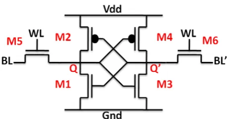
Fig. 1 is a schematic of a conventional 6T SRAM cell (6T1W2B, which stands for 6Transistors, 1Word line, and 2 Bit lines). Both storage nodes (Q and Q’) are statically tied to either VDD or Gnd (hence the prefix static or S). To achieve
this, two inverters (one configured by M1 and M2, another configured by M3 and M4) are cross-coupled – the output of each inverter is the input of the other inverter. Since two cross-coupled inverters constitute a ring oscillator, the storage nodes will settle in a stable state (note that a ring oscillator with odd number of inverters will oscillate). Each storage node is also coupled to one of the two bit lines (BL and BL’) through one of the access transistors (M5 and M6). A single word line (WL) is used to control both access transistors. Through the access transistors, we can read from or write into the storage nodes.
Low Power Dual Word Line 6-Transistor
SRAMs
[image:1.595.311.542.182.303.2]Michael C. Wang, Princeton University
Typically, an SRAM device can perform the following actions: hold, read, and write. We will examine how a 6T SRAM perform each action in connection to Fig. 1.
Hold: when an SRAM is not being written or read, it is in the “hold” state. The word line is asserted to Gnd to turn off access transistors (M5 and M6). The SRAM is now simply a two-transistor ring oscillator. It is easy to see that the storage nodes “lock” each other to one of the supply rails voltage (VDD or Gnd). Deviations from the supply rail voltage will be
eliminated quickly.
Read: before reading a value from the storage nodes, both bit lines (BL) are pre-charged to VDD. The word line is then
asserted to VDD. The storage node that stores a 1 will stay at 1
since it is connected to a pre-charged bit line. The storage node that stores a 0 is statically connected to Gnd and will drain the charges on the bit line, which means that the bit line has just read a 0. Note that at the instant when the word line is turned on, the storage node that stores a 0 will jump to an intermediate voltage because there is now a current path from the bit line to Gnd. The intermediate voltage is determined by voltage dividers constructed by one of the access transistors and the NMOS transistors (M1 or M3) of the cross-coupled inverters. Since the storage nodes are coupled, we do not want the intermediate voltage to jump too high, otherwise it will invert the data stored at the other storage node. Therefore, the NMOS transistors of the cross-coupled inverters are made larger than the access transistors to ensure that the intermediate voltage does not flip the content of the other storage node.
Write: before writing a value, BL (on Q side) will be asserted to a value desired to be written while BL’ (on Q’ side) will be asserted to a value opposite to the value desired to be written. For example, in Fig. 1, if a 0 is desired to be written, then BL will be asserted to Gnd and BL’ will be asserted to VDD. At the instant when the word line turned on,
WL is asserted to VDD to turn on the access transistors M5 and M6, storage node Q will jump to an intermediate voltage. However, as discussed previously, we require the size of NMOS transistors of the cross-coupled inverters to be larger than the access transistors so that the intermediate voltage will not jump too high to invert the content of the other storage node. Therefore, the write operation has to be performed through the side with storage node at 1 and bit line pre-charged to Gnd. In this case, when the word line turned on, there will be a current path between the supply rail VDD
and the bit line pre-charged to Gnd via the PMOS transistor of the cross-coupled inverter and one of the access transistors. We have to size these transistors so that the intermediate voltage will be low enough to flip the content of the other storage node, thus achieving write operation. In other words, the access transistors have to be stronger than the PMOS transistors of the cross-coupled inverters.
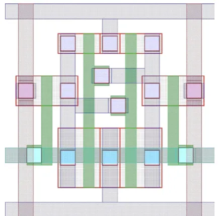
As the above paragraphs demonstrate, we have shown that the driving strength of the transistors in a conventional 6T SRAM cell are ordered as follows: NMOS transistors of the cross-coupled inverters (M1 and M3) > access transistors (M5 and M6) > PMOS transistors of the cross-coupled inverters (M2 and M4). The layout of a 6T SRAM is illustrated in Fig. 2.
III. DUAL WORD LINE DESIGNS
Fig. 3 shows the schematic of 6T SRAM with dual word lines. (6T2W2B). A second word line WL2 is used to control assess transistor M6 so that each access transistor is controlled by a different word line. The motivation of having separating word lines come from the fact that SRAM always reads/writes primarily from one side. For example, write operation is done primarily by forcing a 0 into the cell from one side, and read operation is done primarily by draining charges from one (and only one) of the bit line to Gnd. By having two word lines, we can turn off the access transistor that is not active during read or write operation. In other words, utilizing two word lines enables us to propose a novel power-saving operating scheme.
[image:2.595.317.535.46.261.2]The idea of using two word lines to control each access transistor is not new. Because in a 4T SRAM design, a single word line cannot realize the SRAM functionalities, therefore, a dual word line design is proposed [6]. Nevertheless, the novelty of utilizing dual word line in 6T SRAM not only enables us to come up with a power-saving scheme, but also grants us the ability to shrink cell area by merging both bit lines into a single bit line, which is not possible for the 4T SRAM. The operations of the proposed 6T SRAM with dual word line and dual bit line (6T2W2B) and 6T SRAM with dual word line and single bit line (6T2W1B) will be elaborated later in this section.
[image:2.595.315.547.649.769.2]We will now examine the operating scheme of 6T SRAM with dual word line and dual bit line (6T2W2B).
Hold: both word lines (WL and WL2) are asserted to Gnd to turn off access transistors (M5 and M6) so that the cross-coupled inverters form a two-transistor ring oscillator.
Read: pre-charge BL to VDD, then assert WL to VDD and
turn access transistor M6 off by asserting the second word line WL2 to Gnd. This implies that we will always read from BL (see Fig. 3). If the memory node Q is at 1, BL will remain at VDD. If node Q is at 0, BL will be discharged to Gnd. Thus the
information at node Q is “read” onto BL.
Write: given how SRAM is sized, writing a 1 into a node is accomplished by writing a 0 into its complementary node. To write a 1 into node Q, we assert WL2 to VDD and turn access
transistor M5 off by asserting the word line WL to Gnd. Next, we assert a 0 on BL’ so that node Q’ will be pulled to Gnd, which will then pull node Q to VDD. Since access transistor
M5 is turned off, there is nothing that will prevent Q from being pulled up to VDD. To write a 0 into node Q is done
similarly; we assert WL to VDD and WL2 to Gnd, then assert a
0 on BL so that node Q will be pulled to 0.
Even though there are two word lines, only one is asserted during each read or write operation. Therefore, the 6T SRAM design with dual word line (6T2W2B) does not incur extra switching power consumption on word lines. The advantage of this design comes from the reduction of bit line switching. In read operation, only BL needs to be pre-charged to VDD
(while in the traditional 6T1W2B, both BL and BL’ need to be pre-charged). In write operation, neither BL nor BL’ will be asserted to VDD (while in the traditional 6T1W2B, one of
BL or BL’ will be asserted to VDD).
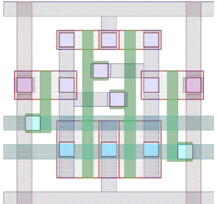
The layout of the 6T SRAM design with dual word line and dual bit line is shown in Fig. 4. By comparing Fig. 4 to Fig. 2, it is easy to see that dual word line design does not incur extra area overhead because the extra word line can be easily routed.
We will quickly review the action done to BL and BL’ during read and write operations. For read operation, BL is pre-charged to VDD; for write 0 operation, BL is asserted to 0,
and for write 1 operation, BL’ is asserted to 0. Note that in any time, only one of BL or BL’ is active; the other is in the “don’t care” state. This suggests that it is possible to merge both BL and BL’ into a single bit line BL, as shown in Fig. 5. We will now describe a new operating scheme for 6T SRAM with dual word line and single bit line (6T2W1B).
Hold: both word lines (WL and WL2) are asserted to Gnd to turn off access transistors (M5 and M6) so that the cross-coupled inverters form a two-transistor ring oscillator.
Read: pre-charge BL to VDD, then assert WL to VDD and
WL2 to Gnd. If the memory node Q is at 1, BL will remain at VDD. If node Q is at 0, BL will be discharged to Gnd. Thus the
information at node Q has been “read” onto BL.
Write: To write a 1 into node Q, we assert WL2 to VDD and
WL to Gnd. Next, we assert a 0 on BL so that node Q’ will be pulled to 0, which will then pull node Q to 1. Since WL is asserted to Gnd to turn off M5, there is nothing that will prevent Q from being pulled up to 1. To write a 0 into node Q is done similarly; we assert WL to VDD and WL2 to Gnd, then
assert a 0 on BL so that node Q will be pulled to 0.
[image:3.595.333.513.54.175.2]The main motivation for a 6T SRAM with dual word line and single bit line design is for cell area reduction. As shown in Fig. 6, we can make both access transistors sit in the same side of the cell to reduce the overall width of the cell. This benefit is exclusive to the single bit line design of a 6T
[image:3.595.60.275.544.745.2]Fig. 4. Layout of a 6T SRAM cell with dual word line and dual bit line in 65nm technology
Fig. 5. Schematic of a 6T SRAM cell with dual word line and a single bit line
[image:3.595.333.518.544.745.2]SRAM, because both access transistors share the same bit line.
IV. SIMULATION RESULTS
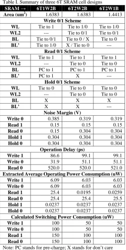
Simulation results for the three SRAM designs (6T1W2B,
6T2W2B, 6T2W1B) are presented in Table 1. In the following subsections, we will explain how to extract three important metrics of an SRAM design: noise margins, power, and delays.
A. Noise Margin Extraction
Noise margin quantifies the amount of voltage noise required at the memory nodes of the SRAM cell to flip the cell’s contents [7]. During read/hold operation, we want the SRAM cell to be as robust as possible so that a sudden disturbance will not change the content in the memory nodes. For example, read noise margin of 0.4V means that during
by less than 0.4V, then we can be sure that after the read operation, the content of Q and Q’ will remain the same, and any disturbance to the voltage in the cell will be eliminated. Therefore, a larger read/hold noise margin is preferred. During write operation, the situation is reversed; we want the content of Q and Q’ be easily switched. Therefore, the write noise margin (more commonly referred to as the “write margin”) is defined as the range of voltage disturbances that will flip the content of the memory nodes. For example, if write margin is 0.5V, then a range of at least 0.5V disturbance in the memory nodes (say 0.1V to 0.6V) will cause their content to flip, thus achieving write operation. The noise margins graphs for all three SRAMs discussed in this paper are plotted in Figures 7, and 8.
[image:4.595.304.556.53.278.2]The exact value of noise margins are extracted by first finding the largest square that fits between the curves traced out by the cross-coupled inverter, and then measuring the length of the square and convert it to voltage, as shown in Table I. Summary of three 6T SRAM cell designs
SRAM → 6T1W2B 6T2W2B 6T2W1B
Area (um2) 1.6383 1.6383 1.4413
Write 0/1 Scheme
WL Tie to 1 Tie to 1/0 Tie to 1/0
WL2 --- Tie to 0/1 Tie to 0/1
BL Tie to 0/1 Tie to 0 / X Tie to 0
BL’ Tie to 1/0 X / Tie to 0 ---
Read 0/1 Scheme
WL Tie to 1 Tie to 1 Tie to 1
WL2 --- Tie to 0 Tie to 0
BL PC to 1 PC to 1 PC to 1
BL’ PC to 1 X ---
Hold 0/1 Scheme
WL Tie to 0 Tie to 0 Tie to 0
WL2 --- Tie to 0 Tie to 0
BL X X X
BL’ X X ---
Noise Margin (V)
Write 0 0.385 0.319 0.319
Read 1 0.15 0.15 0.15
Read 0 0.15 0.304 0.304
Hold 1 0.304 0.304 0.304
Hold 0 0.304 0.304 0.304
Operation Delay (ps)
Write 1 86.6 99.1 99.1
Write 0 31.9 51.1 51.1
Read 0 520.0 520.0 521.0
Extracted Average Operating Power Consumption (uW) Write 1 6.09 6.03 6.03
Write 0 6.09 6.03 6.03
Read 1 25.4 0.0195 0.0259
Read 0 25.4 25.4 25.5
Hold 1 0.0237 0.0237 0.0237
Hold 0 0.0237 0.0237 0.0237
Calculated Switching Power Consumption (uW) Write 1 100 50 50
Write 0 100 50 50
Read 1 150 100 100
[image:4.595.38.290.56.554.2]Read 0 150 100 100 Note: PC stands for pre-charge; X stands for don’t care
Fig. 8. Noise Margin for 6T2W2B and 6T2W1B
[image:4.595.307.555.532.759.2]Figures 7 and 8. The reader can find the exact value of noise margins for these SRAM in Table 1. Simulation results show that 6T SRAM designs with dual word line (6T2W2B,
6T2W1B) suffer 17% reduction in write margin for writing, but gain 103% more read noise margin for reading a 0.
B. Delay Extraction
SRAM delays usually are defined as the time it takes to read or write a value from an SRAM cell. When a node is switching, delay is measured as the time difference between 10% and 90% of the voltage swing. For example, if we are trying to bring node A from 0V to 1V, then the delay is the time it takes for node A to go from 0.1V to 0.9V.
In our simulation, we assumed all the buses (bit line and word line) have 50fF capacitance and all memory nodes have 1fF capacitance. Therefore, it takes much less effort to switch memory nodes than to switch bit line. This is why, in general, delays for write operation are smaller than delays for read operation in SRAMs, because writing into a cell is the same as switching the memory node, and reading from a cell is the same as switching the bit line. Note that for read operation, since the bit line are pre-charged to VDD, there is no
significant current flow and voltage changes across the access transistor if the cell contains a 1. Therefore, read 1 delay is not defined. Simulation results show that 6T SRAM designs with dual word line incur an average 37% increase in write delay (14% increase for writing 1, and 60% increase for writing 0) compared with the traditional single word line 6T SRAM. There is no significant difference in read delay.
C. Power Extraction
In an SRAM operation, power is consumed in two phases: the setup phase and the operation phase.
Energy consumed during the setup phase is dominated by pre-charging/discharging various buses such as bit lines and word lines. Using the formula Ebus = CbusVbusVDD, in which
Cbus is the bus capacitance and Vbus is the change in bus
voltage, we can calculate the energy drawn from the supply by the bus. From this information, we can obtain the average power of an SRAM operation by dividing the clock period. In our simulation, we use a clock with 1ns clock period (or equivalent to 1GHz clock frequency).
The power consumption for the setup phase is reported as “Calculated Switching Power Consumption” in Table 1. In our simulation, we assumed 50fF capacitance for all buses (including supply rails for from SRAMs that utilizes multiple voltage supplies).
Power consumed during the operation phase is dominated by active power and leakage power. Active power is the power consumed when both pull-up and pull-down network are active, creating a direct current path from VDD to ground.
Leakage power is the power consumed when charges “leak” through a transistor that is off. Measuring the active and leakage components of power consumption separately is very difficult. Therefore, we will measure the aggregated power consumption by using the .PRINT POWER command in HSPICE, which will give us the total power drawn from all voltage sources. The result is shown as “Extracted Average Operating Power Consumption” in Table 1. Simulation results show that 6T SRAM with dual word line designs achieves an average 17% reduction in operating power consumption and, most importantly, a 42% reduction in bit
line and word line switching power consumption compared with the traditional single word line 6T SRAM.
Fig. 9 shows the operating power consumption and switching power consumption of 6T1W2B, 6T2W2B, and
6T2W1B categorized by SRAM operations.
V. CONCLUSION
Continuing technology scaling puts a limit on how much supply voltage can be scaled. Therefore, new architectures are needed to reduce power consumption in integrated circuits. In the case of SRAM, one seemingly counterintuitive approach is to utilize a second word line, which leads to the development of 6T SRAM with dual word line. The new SRAM operating scheme, enabled by the addition of the second word line, gives us significant power reduction by reducing the amount of switching on bit lines. Extending this operating scheme also allows us to propose a dual word line and a single bit line design that achieves smaller area while retaining all of the power saving advantages. For a small penalty in delay, 6T SRAMs with dual word line are attractive alternatives as memory storages for applications that do not require high clock frequency.
REFERENCES
[1] Nayak, A., Haldar, M., Banerjee, P., Chen, C., and Sarrafzadeh, M.: 'Power optimization of delay constrained circuits', ASIC/SOC Conference, 2000, pp. 13-16
[2] Keerthi, R., and Chen, C.: 'Stability and Static Noise Margin Analysis of Low-Power SRAM', Instrumentation and Measurement Technology Conference Proceedings, 2008, pp. 1681-1684
[3] Aly, R., Faisal, M., and Bayoumi, A.: ‘Novel 7T SRAM cell for low power cache design’. Proc. IEEE SOC Conf, 2005, pp. 171-174 [4] Jain, S.K., and Agarwal, P.: ‘A low leakage and SNM free SRAM cell
design in deep sub micron CMOS technology’. Proc. 19th International Conference on VLSI Design held jointly with 5th International Conference on Embedded Systems Design, 2006, pp. 495-498 [5] Liu, Z., and Kursun, V.: 'Characterization of a Novel Nine-Transistor
SRAM Cell', VLSI Systems, IEEE Transactions on, 2008, 16, pp. 488-492
[6] Mazreah, A.A, Manzuri Shalmani, T., Barati, H., and Barati, A.: ‘A Novel Four-Transistor SRAM Cell with Low Dynamic Power Consumption’. Proc World Academy of Science, Engineering and Technology, 2008