Iranian Journal of Electrical and Electronic Engineering, Vol. 15, No. 2, June 2019 258
A Low Voltage Low Power CMOS Implementation of Second
Generation Orderly Current Buffer
S. J. Azhari*
(C.A.)and M. Zareie*
Abstract: In this paper, a novel low voltage low power current buffer was presented. The proposed structure was implemented in CMOS technology and is the second generation of OCB (orderly current buffer) called OCBII. This generation is arranged in single input-single output configuration and has modular structure. It is theoretically analyzed and the formulae of its most important parameters are derived. Pre and Post-layout plus Monte Carlo simulations were performed under 0.75 V by Cadence using TSMC 0.18 µm CMOS technology parameters up to 3rd order. The proposed structure could expand and act as a dual output buffer in which the second output shows extremely high impedance because of its cascode configuration. The results prove that OCBII makes it possible to achieve very low values of input impedance under low supply voltages and low power dissipation. The most important parameters of 1st, 2nd and 3rd orders, i.e. input impedance (R
in), -3 dB bandwidth (BW), power dissipation (Pd) and output impedance (Ro) were found respectively in Pre-layout plus Monte Carlo results as:
1st order: R
in (52.4 Ω), BW (733.7 MHz), Pd (225.6 µW), Ro (105.6 kΩ) 2nd order: R
in (3.8 Ω), BW (576.4 MHz), Pd (307 µW), Ro (106.4 kΩ) 3rd order: R
in (0.34 Ω), BW (566.9 MHz), Pd (535.6 µW), Ro (118.2 kΩ) And in Post-layout plus Monte Carloresults as:
1st order: R
in (59.9 Ω), BW (609.6 MHz), Pd (212.4 µW), Ro (106.9 kΩ) 2nd order: R
in (11.3 Ω), BW (529.3 MHz), Pd (389.9 µW), Ro (109.8 kΩ) 3rd order: R
in (5.8 Ω), BW (526.5 MHz), Pd (514.5 µW), Ro (125.5 kΩ)
Corner cases simulation results are also provided indicating well PVT insensitivity advantage of the block.
Keywords: Second Generation OCB, Current Buffer, Extremely Low Input Impedance, Very Wide Bandwidth Current Buffer, Current Mode.
1 Introduction1
HE current mode approach of analog circuit design has recently gained considerable attention. High slew rate, high bandwidth, simple circuitry and low voltage operation are some of advantages of current mode circuits compared to voltage modes [1-8]. Current buffers are one of the main building blocks of current mode signal processors which find wide applications in
Iranian Journal of Electrical and Electronic Engineering, 2019. Paper first received 30 April 2018 and accepted 20 August 2018. * The authors are with the Department of Electrical Engineering, Iran University of Science and Technology (IUST), Tehran, Iran. E-mails: [email protected] and [email protected]. Corresponding Author: S. J. Azhari.
realizing filters, oscillators, signal conditioners, current amplifiers etc. [9-18].
Current buffers are characterized by low input impedance ideally zero. The authors of [13] introduced, a novel type current buffer being called Orderly Current Buffer, OCB, which has the potential of producing low input impedance. The orderly current buffer have regular structure in which a core cell is repeated as many times as required to produce very low input impedance current buffers. The first generation of OCB called OCBI was implemented in fully differential structure in BJT technology [13]. The weakness of OCBI was its large power consumption which was reported as 10.3mW for 3rd order. In addition, due to the dominance of CMOS technology, implementing BJT type OCB may not be cost effective. To provide more
T
Iranian Journal of Electrical and Electronic Engineering, Vol. 15, No. 2, June 2019 86 structural flexibility and freedom the single ended
arrangement is examined which shows excellent frequency operation and results in lower power consumption compared to OCBI. Favorably, the simple structure and lower power consumption of OCBII the implementation of its higher orders possible.
2 Circuit Analysis and Discussion
2.1 First Order Current Buffer (OCBII)
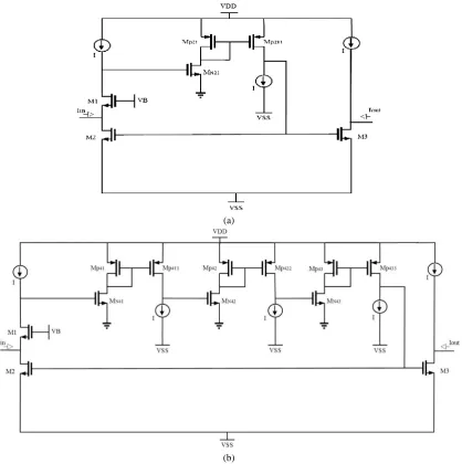
The circuitry of the 1st-order OCBII is shown in Fig.1. As it is seen an active feedback loop consisting of common gate input transistor M1, current source I and gain transistor M2 is such arranged that initially delivers most of Iininto the source node of M1 (at input node,
rsM1<<roM2). It is then amplified by M2 and fed back to the input node causing Iin to be mostly sunk by drain junction of M2 rather than being sourced into source junction of M1, at last. The input current which is such sunk by M2 is mirrored to the buffer’s output node by M3. The order of the OCBII is taken after the number of the gain blocks of the feedback loop (i.e. M2 here). The diode connected transistor MD is used for appropriate level shifting.
2 2
1 dBM gsM
C C C
1
2 gsM
C C
1 1 2 3 2
3
3
1
2 2
M M M M M
M
gd db gs gs dg dg
C C C C C C
C C
3 3
4 dgM dbM
C C C
1 /
I I MD I I
B O O m O O
R R R g R R (1)
In (1), gm, CI, Cgs, Cdb, Cdg, rO, ROI and ROI' denotes the transconductance of the related transistor, output capacitance of current source I, gate-source capacitance, drain-body capacitance, drain-gate capacitance, output impedance of related transistor, output impedance of I current source and output impedance of I' current source respectively. The equivalent resistance of diode connected transistor D is also omitted for simplicity. According to feedback theory we have:
inf
1
in Z Z
T
(2)
where, Zin is the open loop input impedance, T is the feedback loop gain and Zinf is closed loop input impedance. By ignoring higher order poles and zeroes, the loop gain T can be found from:
2
2
2 3
1
1
1
1
1 1
1
M
M
M
o f
B m
in o B
m M
r I
T R g
I r sC R
g
K
S P
(3)
while
2
2 2
1
1 1
M
M
M
M
o
B m o
m
r
K R g
r
g
(3.1)
11 B. 3
P R C (3.2)
Referring to (3) through (3.2), P1 is the dominant pole of T and K1 is the DC value of loop gain.
Zin (open loop input impedance) and Zinf(closed loop one) can be found as:
Fig. 1 1st order OCBII.
Fig. 2 Open loop small signal equivalent circuit of 1st order OCBII.
Iranian Journal of Electrical and Electronic Engineering, Vol. 15, No. 2, June 2019 86 1 2 1 1 1 M in m Z S g P (4)
1 12 1 2
1
M
m
P C C
g (4.1)
1 1 12 1 1
1 1 1 1 1 1 M in in f m S Z P Z
T K g S S
P K P
(5)
As it is seen from (5), Zinf has a zero equal to the dominant pole of T in (3) and two much larger poles. On the other hand, the DC value of Zinf is K1 times lower than that of a simple common gate structure (i.e. 1/gmM1) with a very wide bandwidth (here in worst case, P1) depending on the utilized transistors.
Now for Aif, using the feedback theory gives:
1
1
1
2 1 1
1 1 1 1 1 1 M in in f m S Z P Z
T K g S S
P K P
(6)
Eq. (6) shows that the DC value of Aif is close to unity while its bandwidth is:
1 1
BW K P (6.1)
Multiple output version of 1st order OCBII can also be simply implemented. Fig. 3 shows the two output version of OCBII. The first output is composed of simple current mirror with moderately high output impedance while the second output is composed of cascode current mirror exhibiting very high output impedance.
2.2 Higher Orders Structure (OCBII)
The repeating part of higher orders is common source arrangement as is shown in Fig. 4 in which MNni provides high loop gain and PMOS current mirror composed of MPni-MPnii simply transfer currents to the next stages. In the gain transistor, N indicates the type of transistor, i.e. NMOS, the index n is determined by the order of current buffer and i is the transistors’ number. For the current mirror transistors, index P represents the type of transistor, i.e. PMOS, indexes n and i represents buffers order and transistors number, respectively. The first order is preceded by 2nd order as is shown in Fig. 5(a) which is implemented by adding one repeating part to the first order structure. As can be seen, n is replaced by 2 indicating the order of current buffer. In OCBII, the order of the buffer simply indicates the number of the used repeating part. Based on this discussion, the circuitry of 4th order of OCBII is shown
in Fig. 5(b).
The open loop gain of the nth order OCBII can be found as:
2 2 1 1 11 3 4
1
1
1 1 1
M Ni M M n o m B o m n n r
T g R
r g
S S S
P P P
(7)
3 1 2I Pnii MPnii Pnii Mni
Mni
O o db dg gs dg
P R r C C C
C
(7.1)
4
1
1
Mpni Mpni MNni Mpni
Pni
MNni MPnii
gs gs db db m
dg gd
P C C C C
g
C A C
(7.2)
In (7.2), A is the miller effect on the drain gate capacitance of MPnii transistor and is defined as:
||
MPnii MPnii I
m o O
A g r R (7.3)
In frequency domain each repeating cell adds two poles to the 1st order structure according to (7). One of the extra poles is produced by gain transistor and the other is related to current mirror.
Fig. 3 Multiple output version of OCBII.
Fig. 4 Common source arrangement as the repeating part of higher orders.
Iranian Journal of Electrical and Electronic Engineering, Vol. 15, No. 2, June 2019 85 (a)
(b)
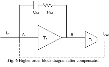
Fig. 5 Higher order OCBII; a) 2nd order and b) 4th order. 2.3 Higher Orders Compensation
As is done in OCBII, the higher order compensation is done by connecting compensation capacitor between input node and node B according to the block diagram of Fig. 6 in which RB is the equivalent resistant of node B. In Fig. 6 we have:
1 1 2
3 4
1 1
n
n n
K T
S S
P P
2
1 2
1
1
1
M
M
M
M
n O
n m B
o
m
r
K g R
r
g
2
1 4
1 1
K T
S S
P P
2
M
B m
K R g (8)
Using the block diagram of Fig. 6 it can be proved that the loop gain after compensation is:
1
2 2
1 2
1
1 M M id
M e
M e
T SR C
A T
C r
S ST C r
P
(9)
The open loop transfer function of (9) can be simplified to:
2 1
1 1
n
id n
d nd
K K
A
S S
P P
(10)
where
1
1
1
M
d n M m
P K C
g
(10.1)
Iranian Journal of Electrical and Electronic Engineering, Vol. 15, No. 2, June 2019 86
Fig. 6 Higher order block diagram after compensation.
1 2
2 1
1 2 3 4
n n n
nd n
P K P P P P (10.2) The dominant pole is much smaller than the non-dominant ones resulting in a proper phase margin. However the value of compensation capacitor is chosen such that the unity gain frequency of (10) gets smaller than non-dominant poles.
The open loop input impedance can also be found from (11).
2.4 Closed Loop Parameters of Higher Orders
Using (8)-(11), the closed loop parameters are found as follows:
21 1
1 n
id f n
n df KK A KK S P (12) 2 1
2n n
df d nd
P P P (12.1)
1 1 2 3 4 2 1 11 1 1
1 f Q id n m n n M M n df R KK g S S SR C P P S P (13)
3 Simulation Results and Discussion
To study the practical behavior of the block it is simulated up to 3th order for the single output configuration and the dual one. Both pre and post-Layout plus Monte Carlo (with 100 number of runs under mismatch and process variation) simulations are carried out by Cadence using TSMC 0.18 µm CMOS
Table 1 Transistor aspect ratio of the proposed circuit. Transistors W[µm]/L[µm]
Non-Repeated Ones
M1 80/0.5
M2,M3 16/0.4
MD 30/0.18
M4 17.1/0.4
M5 17.1/0.18
Repeated Ones MNni 60/0.18
MPni,MPnii 30.51/0.18
Table 1 The used elements’ values.
Element Value
I 30 [µA]
I' 20 [µA]
I'' 50 [µA]
VDD & VSS 0.75 [V]
VB 0 [V]
CM 1st Not Required
2nd 130 [fF]
3rd 500 [fF]
technology parameters under ±0.75 V supply voltage. The aspect ratios of transistors and the used element values are given in Tables 1 and 2, respectively.
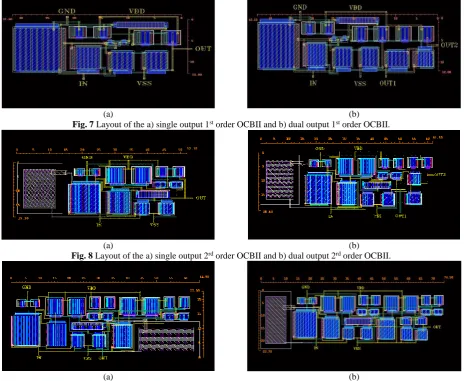
The layout views of the OCBII are shown for the single output and dual output of the 1st order in Fig. 7, of the 2nd order in Fig. 8, and of the 3rd order in Fig.9. The proper frequency performance for a versatile current buffer defined as it shows low input impedance to wide bandwidth frequency input signals with low power consumption. The dual output structure show more output impedance from the cascode current mirror with the same input impedance as the single output structure. It only consumes a bit more power (about 70 µW as a mean value for the 1st, 2nd and 3rd orders) than the single output structure and also shows a wide bandwidth. The figures containing frequency bandwidth are responses of the single output design as the main structure.
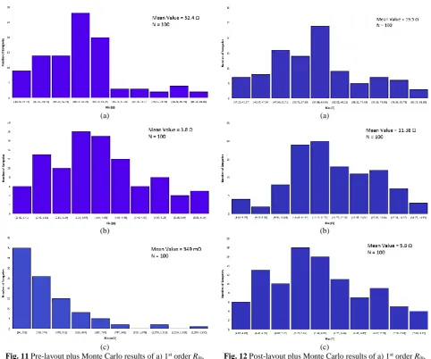
The stimulated frequency performance of the input impedances are 51.5 Ω, 3.2 Ω and 0.25 Ω for the 1st, 2nd and 3rd orders, respectively, and shown in Fig. 10. The Pre-layout plus Monte Carlo input impedances of 1st, 2nd and 3rd order OCBII are respectively shown as 52.4 Ω, 3.8 Ω and 0.34 Ω in Figs. 11(a)-(c), respectively. The post-layout plus Monte Carlo results of input impedances are also shown in Figs. 12(a)-(c), which are 59.5 Ω, 11.38 Ω and 5.8 Ω for the 1st, 2nd and 3rd orders, respectively.
1
1 2
3 4
1 2 1 2
2 '
2 1 3 4 1 3 4
1 . 1 1
1
1 1 1 1 1 1
M
n n
M M
id n n n n
m M e
n M e
S S
S R C
P P
R
g C r S S S S S S
S SK C r
P P P P P P P
(11)
Iranian Journal of Electrical and Electronic Engineering, Vol. 15, No. 2, June 2019 86
(a) (b)
Fig. 7 Layout of the a) single output 1st order OCBII and b) dual output 1st order OCBII.
(a) (b)
Fig. 8 Layout of the a) single output 2rd order OCBII and b) dual output 2rd order OCBII.
(a) (b)
Fig. 9 Layout of the a) single output 3rd order OCBII and b) dual output 3rd order OCBII.
Fig. 10 Simulated Rin of the 1st to 3rd order OCBII. Fig. 13 shows the excellent frequency performance of
the unity gain Ai with 737 MHz, 581.9 MHz and 572 MHz, -3 dB bandwidths for the 1st, 2nd and 3rd orders in simulations results. Pre-layout plus Monte Carlo with bandwidth of 733.7 MHz, 576.4 MHz and
567.4 MHz for 1st, 2nd and 3rd order shows proper robustness to process variations and non-idealities. These results are also shown in Figs. 14(a)-(c), respectively.
Iranian Journal of Electrical and Electronic Engineering, Vol. 15, No. 2, June 2019 85
(a) (a)
(b) (b)
(c) (c)
Fig. 11 Pre-layout plus Monte Carlo results of a) 1st order R
in,
b) 2nd order R
in, and c) 3rd order Rin.
Fig. 12 Post-layout plus Monte Carlo results of a) 1st order R
in,
b) 2nd order R
in, and c) 3rd order Rin.
Fig. 13 Ai frequency performance in simulation results of 1st to 3rd order OCBII.
Iranian Journal of Electrical and Electronic Engineering, Vol. 15, No. 2, June 2019 86
(a) (a)
(b) (b)
(c) (c)
Fig. 14 Pre-layout plus Monte Carlo results of a) 1st order -3 dB BW, b) 2nd order -3 dB BW, and c) 3rd order -3 dB BW.
Fig. 15 Post-layout plus Monte Carlo results of a) 1st order -3 dB BW, b) 2nd order -3 dB BW, and c) 3rd order -3 dB BW.
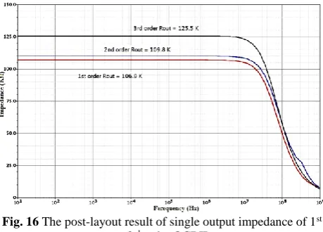
Fig. 16 The post-layout result of single output impedance of 1st to 3rd order OCBII.
Fig. 17 The post-layout result of the high-output impedance structure of 1st to 3rd order OCBII.
Iranian Journal of Electrical and Electronic Engineering, Vol. 15, No. 2, June 2019 87
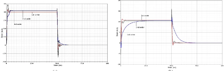
(a) (b)
Fig. 18 a) Simulated step response of 1st to 3rd order OCBII and b) Post-layouted step response of 1st to 3rd order OCBII.
Table 3 Post-layout corner case simulation results of 1st to 3rd orders of OCBI.
Process Corners TT FF SS FS SF
Temperature [°C] 27 -25 75 50 0
Supply Voltage [V] 0.75 0.825 0.675 0.75 0.75
OCBII First Order BW [MHz] 616.6 1370 255.13 403.9 776
Rin [Ω] 58.6 27.4 138.6 56.6 68.2
OCBII Second Order BW [MHz] 534.7 948.3 236.2 497.9 486.6
Rin [Ω] 10.1 9.8 32.5 7.5 30.16
OCBII Third Order BW [MHz] 530.1 896 221.1 474.8 480.9
Rin [Ω] 5.1 4.06 15 5 10
Table 4 Comparison between the proposed OCBII with some related artworks. Ref./Year Rin [Ω]
f -3dB [MHz]
Rout
[kΩ]
Power Consumption
[mW]
Voltage Supply
[V]
Number of Elements
FOM [MHz/µW]
Technology
(CMOS) [μm] Simulation
[14]/2016 18.33 4.5 700 0.051 1.8 1>>11 <<0.3×10³ 0.18 Simulation
[20]/2008 50 80 102 - 0.75 2> 18 <0.4×10² 0.18 Simulation
[21]/2013 3.7 450 127 1.02 1.65 28 0.5×10³ 0.35 Simulation
[19]/2009 56.5 24.6 153 0.27a 0.75 2> 18 <0.13×10² 0.18 Post-Layout [22]/2018 597 464.5 59 0.510a 0.6 2> 12 <0.75×10 0.18 Post-Layout
P
ro
p
o
se
d
b
1st 52.4 733.7 105.6 0.225 0.75 11 0.6×10³ 0.18
Pre-Layout Plus Monte
Carlo
2nd 3.8 576.4 106.4 0.307 0.75 14 0.38×10⁴ 0.18
3rd 0.34 566.9 118.2 0.535 0.75 21 0.2×10⁵ 0.18
1st 59.9 609.6 106.9 0.212 0.75 11 0.46×10³ 0.18
Post-Layout Plus Monte
Carlo
2nd 11.3 529.3 109.8 0.289 0.75 14 0.12×10⁴ 0.18
3rd 5.8 526.5 125.5 0.514 0.75 21 0.1×10⁴ 0.18
a Calculated
b All of the results are related to single output structure.
1 The self-biased current follower of [14] has an operational amplifier in its structure which the inner design of that was not available;
so, it is not possible to find the exact number of elements.
2 These blocks contain some current sources whose detailed structure are not available. To have a fair comparison, it is assumed that
any current source made of only one transistor.
To validate the time domain response of the OCBII, its response to a step input with amplitude of 10 µA for 1st to 3rd orders are examined. The results for regular simulations and for the post-layout simulations are shown in Figs.18 (a) and 18(b), respectively which proves the OCBII’s stability. Moreover, corner cases simulation after post-layout, for major parameters are also studied and reported in Table 3 which shows the
robust performance of proposed current buffer.
Table 4 summarizes the performances of the second generation orderly current buffer and compares them to several recently reported works.
The comparison also includes the figure of merit (FOM) commonly used for current amplifiers performance comparison and defined as (14). However, one should take account into the fact that both of the pre
Iranian Journal of Electrical and Electronic Engineering, Vol. 15, No. 2, June 2019 88 and post layout simulations in this work are plus Monte
Carlo, while the related artworks did not define the impact of Monte Carlo simulations on the final results, so the high FOM results of OCBII shows the definite superiority of this work.
out in
R BW
R Power
FOM
Number of Elements
(14)
To have a fair comparison, authors have considered the not-available parameter of related works as same as the values reported for the 1st order OCBII.
4 Conclusion
In this paper circuitries of 1st to 3rd orders are shown leading to the way of forming the second generation of OCBII in CMOS technology. It is formed in single input single output arrangement. The most important parameters of the proposed circuit are formulized and the merits are discussed. The simulations of the 1st to 3rd orders of OCBII are carried out by Cadence using 0.18 µm TSMC CMOS parameters. To evaluate the impact of PVT non-idealities on the presented work, the corner cases with temperature analysis and both the pre– layout and post-layout plus Monte-Carlo simulations are performed. Simulation results show that OCBII makes it possible to implement low power wide bandwidth current buffers with low input impedance by a simple structure.
Acknowledgment
The authors would like to appreciate Dr. Leila Safari for her valuable input at the beginning of the OCB concept.
References
[1] M. Altun and H. Kuntman, “Design of a fully differential current mode operational amplifier with improved input–output impedances and its filter applications,” AEU-International Journal of
Electronics and Communications, Vol. 62, No. 3,
pp. 239–244, 2008
[2] M. A. Eldeeb, Y. H. Ghallab, Y. Ismail, and H. Elghitani, “Low-voltage subthreshold CMOS current mode circuits: Design and applications,”
AEU-International Journal of Electronics and
Communications, Vol. 82, pp. 251–264, 2017.
[3] H. Faraji Baghtash, K. Monfaredi and A. Ayatollahi, “A novel ±0.5 V, high current drive, and rail to rail current operational amplifier,” Analog
Integrated Circuits and Signal Processing, Vol. 70,
No. 1, pp. 103–112, 2011.
[4] I. M. Filanovsky, J. K. Järvenhaara, and N. T. Tchamov, “On design of low-voltage CMOS current amplifiers,” in IEEE 57th International
Midwest Symposium on Circuits and Systems
(MWSCAS), pp. 563–566, 2014.
[5] B. Pankiewicz, “Multiple output CMOS current amplifier,” Bulletin of the Polish Academy of
Sciences Technical Sciences, Vol. 64, No. 2,
pp. 301–306, Jan. 2016.
[6] F. Esparza-Alfaro, S. Pennisi, G. Palumbo and A. Lopez-Martin, “Low-power class-AB CMOS voltage feedback current operational amplifier with tunable gain and bandwidth,” IEEE Transactions on
Circuits and Systems II: Express Briefs, Vol. 61,
No. 8, pp. 574-578, 2014.
[7] C. Toumazou, F. J. Lidgey, and D. G. Haigh, eds.
Analog IC design: The current mode approach.
U.K.: Patter Peregrines Ltd, On Behalf of IEE, 1993. [8] J. A. Martínez-Nieto, M. T. Sanz-Pascual, N. J. Medrano-Marqués, and B. Calvo-López, “Self-biased class AB CMOS current buffer.” in IEEE 7th
Latin American Symposium on Circuits & Systems
(LASCAS), pp. 255–258, 2016.
[9] G. D. Cataldo, R. Mita, and S. Pennisi, “High-speed CMOS unity-gain current amplifier,”
Microelectronics Journal, Vol. 37, No. 10,
pp. 1086–1091, 2006.
[10]E. Arslan, S. Minaei, and A. Morgul, “On the realization of high performance current conveyors and their applications,” Journal of Circuits, Systems
and Computers, Vol. 22, No. 03, p. 1350015, 2013.
[11]L. N. Alves and R. L. Aguiar, “A differential current-conveyor based buffer for high-bandwidth, low-signal applications,” in The 6th IEEE
International Conference on, Electronics, Circuits
and Systems, Vol. 2, pp. 903–906, 1999.
[12]E. Yuce and H. Alpaslan, “New CMOS based current follower and its applications to inductor simulator and band-pass filter,” Indian Journal of
Pure & Applied Physics (IJPAP), Vol. 54, No. 8,
pp. 511–516, 2016.
[13]S. J. Azhari and L. Safari, “The orderly current buffer, OCB: An innovative block with extremely low input impedance and high CMRR,” World
Academy of Science, Engineering and Technology,
Vol. 61, pp. 114–124, 2010.
[14]R. Senani and S. S. Gupta, “Novel sinusoidal oscillators using only unity-gain voltage followers and current followers,” IEICE Electronics Express, Vol. 1, No. 13, pp. 404–409, 2004.
Iranian Journal of Electrical and Electronic Engineering, Vol. 15, No. 2, June 2019 89 [15]A. Ü. Keskin, D. Biolek, E. Hancioglu, and
V. Biolková, “Current-mode KHN filter employing current differencing transconductance amplifiers,”
AEU-International Journal of Electronics and
Communications, Vol. 60, No. 6, pp. 443–446,
2006.
[16]H. Alzaher, “Current follower based reconfigurable integrator/differentiator circuits with passive and active component’ reuse,” Microelectronics Journal, Vol. 46, No. 2, pp. 135–142, 2015.
[17]H. Alzaher and N. Tasadduq, “Realizations of CMOS fully differential current followers/amplifiers,” in IEEE International
Symposium on Circuits and Systems, pp. 1381–
1384, 2009.
[18]E. Ergun and M. Ulutas, “Low input impedance current-mode allpass and notch filter employing single current follower,” in 14th International
Conference on Mixed Design of Integrated Circuits
and Systems, 2007.
[19]C. Cakir, S. Minaei, and O. Cicekoglu, “Low voltage low power CMOS current differencing buffered amplifier,” Analog Integrated Circuits and
Signal Processing, Vol. 62, No. 2, pp. 237–244,
2009.
[20]C. Cakir and O. Cicekoglu, “Low-voltage high-performance CMOS current differencing buffered amplifier (CDBA),” Ph.D. Research in
Microelectronics and Electronics, 2008.
[21]E. Arslan, “Self-biasing high precision CMOS current subtractor for current-mode circuits,”
Advances in Electrical and Computer Engineering,
Vol. 13, No. 4, pp. 19–24, 2013.
[22]S. Kumari and M. Gupta, “A new CMOS design of high transconductance current follower transconductance amplifier and its applications,”
Analog Integrated Circuits and Signal Processing,
Vol. 95, No. 2, pp. 325–349, 2018.
S. J. Azhari received the B.Sc. degree in Electronic Engineering from Iran University of Science and Technology (IUST), Narmak, Tehran, the M.Sc. degree in Electronic Instrumentation and Measurement from Victoria University of Manchester, U.K., and the Ph.D. degree in Electronics from UMIST, U.K., in 1975, 1986, and 1990, respectively. He joined IUST as a Teaching and Research Assistant in 1975. He is the founder of Electronic Research Center (ERC) of IUST. Currently, he is a Professor in electronic engineering (since 2016) working in Electrical Engineering Faculty and Electronic Research Center of IUST. He is interested in circuit and system design especially in current-mode field, electronic instrumentation and measurement, semiconductor devices and sensor technology. He is the author of more than ten textbooks in electronics, the author or co-author of about sixty papers, and the designer or codesigner of many electronic instruments. Prof. Azhari is a Member of the Iran Electrical Engineering Society. He was the recipient of the O.R.S Award (U.K.) during 1987-1990.
M. Zareie was born in Hamadan, Iran in 1992. She received the B.Sc. degree in Electrical Engineering from Buali-Sina University, Iran, in 2014 and currently she is the M.Sc. student of Electrical Engineering at Iran University of Science and Technology (IUST). Her research interests are low power analog integrated circuit design especially current mode ones. She is currently with IC Design Laboratory at Electronic Research Center (ERC) of IUST.
© 2019 by the authors. Licensee IUST, Tehran, Iran. This article is an open access article distributed under the terms and conditions of the Creative Commons Attribution-NonCommercial 4.0 International (CC BY-NC 4.0) license (https://creativecommons.org/licenses/by-nc/4.0/).