Please cite this article as: P. Karuppanan, K. Anuradha, Study and Analysis of A Simple Self Cascode Regulated Cascode Amplifier, International Journal of Engineering (IJE), IJE TRANSACTIONS A: Basics Vol. 31, No. 10, (October 2018) 1633-1641
International Journal of Engineering
J o u r n a l H o m e p a g e : w w w . i j e . i rStudy and Analysis of A Simple Self Cascode Regulated Cascode Amplifier
P. Karuppanan*, K. Anuradha
Department of Electronics and Communication Engineering, Motilal Nehru National Institute of Technology Allahabad, India
P A P E R I N F O
Paper history:
Received 29 July 2017
Received in revised form 26 April 2018 Accepted 26 April 2018
Keywords: Self Cascode Regulated Cascode
Self Cascode Based Regulated Cascode Simple Self Cascode Regulated Cascode
A B S T R A C T
This article proposed a simple self cascode RGC amplifier configuration to increase the gain and bandwidth. The cascode amplifier eliminates the miller capacitance between input and output and facilitates high gain, high input and output impedance with high bandwidth. However, the cascode amplifier requires relatively high supply voltage for proper operation and it decreases the output voltage swing by overdrive voltage. These issues are overcome by self cascode based RGC amplifier; even though it has low bandwidth due to the presence of one of its pole at low frequency. The bandwidth and output impedance of the conventional RGC has increased using a split length compensation technique. To improve the overall performance of the amplifier, introduced a simple self cascode RGC without using additional passive elements. The expression of gain and output impedance for the proposed amplifier is derived using small signal analysis. The calculated value of voltage gain for the projected circuit is 58.37 dB which is more than the self cascode based RGC. The power dissipation of the proposed circuit is 1.07 µWatt and it was compared with CS, cascode, self cascode and SC based cascode, RGC, SC based RGC amplifiers.
doi: 10.5829/ije.2018.31.10a.04
1. INTRODUCTION1
In recent years, the requirement of low power and portable electronic devices is increasing due to its wide range of applications. The complementary metal oxide semiconductor (CMOS) technology is suitable for low power, high-speed analog and mixed signal circuit design. It arise new challenges in designing of analog VLSI circuits as the demand for compact size, high reliability and high gain amplifier [1]. To design a single stage amplifier with high gain is too difficult and this problem needs to be solved. Currently, many researchers have reported several techniques to increase the gain of amplifiers and it can be designed using long channel transistor [2, 3]. However, the cutoff frequency of the transistor is inversely proportional to the square of the channel length. As a result, the longer channel length is not a suitable solution since it will not work for low-frequency applications [4]. To eliminate these drawbacks, Cascode transistors has been proposed and it also causes a loss in linear output swing of the
*Corresponding Author Email: [email protected] (P Karuppanan))
amplifiers. The output swing can be improved while connecting a series combination of two transistors in which the upper transistor has longer channel length than a lower transistor. This structure is known as self cascode or composite transistor and it has been proposed by Comer [5]. The self cascode technique makes the designing of amplifier circuit simple, which provides high voltage gain that can be used in op amps with low power dissipation [6]. For the further improvement of the gain of cascode amplifier was introduced in regulated cascode (RGC) amplifier [7]. The regulated cascode provides high gain; however, the bandwidth of this circuit is reduced due to one pole of the RGC located at a given low frequency. There are several techniques have been disclosed to improve the bandwidth. As described in the literature, the self cascode is the solution to most of the problem like bandwidth, output voltage swing, power dissipation [8]. Consequently, the cascode transistor is replaced by self cascode transistor in the conventional RGC amplifier which is called as self cascode based regulated cascode amplifier [9].
cascode amplifier in order to improve the gain. The parameters like voltage gain, power dissipation, 3-dB bandwidth, output voltage swing were calculated. The calculated value of voltage gain for the proposed circuit is 58.37 dB and the power dissipation obtained is 1.071µWatt. The expression for the voltage gain and output impedance is calculated using small signal model.
2. SELF CASCODE AMPLIFIER
To fulfill the requirement of low power dissipation and high-performance amplifier, self-cascode amplifier technique is introduced which does not need high supply voltage [9]. It provides high output impedance to achieve high gain; hence it is useful in low-voltage analog circuit design.
A self-cascode amplifier consists of two transistors in which both the transistors are biased by a single input supply as shown in Figure 1, which is similar to a single composite transistor. When W/L ratio for both transistors is the same, M1 will work in triode region and M2 will operate in the active region and thus the single composite transistor works like a common source amplifier with high voltage gain. But when W/L ratio of M2 is greater than that of M1, M1 will operate in triode region i.e. it can be replaced by a linear resistor whereas M2 will operate in saturation region which again increases the voltage gain.
The W/L ratio of upper transistor M2 must be larger than that of lower transistor M1 for proper operation of self cascode structure i.e., m>1 [10, 11]. The voltage gain of self cascode amplifier is given by the following expression:
1 2 2
2 1 2 2
2 1
( )
1
m m o L
V
o m m gs
L gs m
g g r R
A s
r g g s C
R sC g
(1)
where, gm1and gm2 are the transconductance of transistor
M1 and M2 respectively. RLis the load resistance of the
self cascode amplifier. Cgs2is gate source capacitance of transistor M2,r02 is the output resistance of transistor M2.
Figure 1. Self cascode amplifier
3. REGULATED CASCODE AMPLIFIER
The RGC circuit has an extra MOS transistor which forms a feedback loop between transistors M1 and M2 that structure is shown in Figure 2. It is connected to maintain constant drain to source voltage of input transistor M1and to maintain the biasing of transistor
M2. To design a circuit with larger bandwidth, minimum
feature size should be followed.
A regulated cascode (RGC) amplifier is used to reduce the input impedance so that the dominating pole of the amplifier will not be located at the input. In the RGC circuit, transistor M1 converts the input voltage Vin into a drain current Id2, that flows through the drain-source path of M2 to the output terminal [12]. The output resistance of MOS transistor decreases with increase in channel length modulation. Thus, to obtain a high output resistance, i.e., to avoid the effect of channel-length modulation of M1, the respective drain-source voltage must be kept stable [13]. In the regulated cascode, this is obtained by a feedback loop consisting of an amplifier (M3). In this way, the drain-source voltage of M1 is regulated to a fixed value. Note that the feedback mechanism upon which the stabilization is based works even if M2 is driven into the ohmic region. It can be concluded that input impedance has been reduced by a factor of (1+gm1Rb) relative to a common gate input stage [14]. To obtain a more small input impedance, it is desirable to increase the factor
(1+gm1Rb), which can be done by increasing the
transconductance of the transistor M1 (gm1) or the bias resistor (Rb). These two parameters can be increased upto a certain limited value, because an increase in Rb would require a decrease in the bias current Id2 in order to keep M2 in the active region. The expression for voltage gain of RGC is given as follows:
1 3
2 2
0
2
3 2 2
4 4
2 3 2 }
3 0
) 2
3
{ }
( )
{ ( )
( )
m v
o b o gs o b
gs g
l m m b b
s m
gs m o b m m o b
o g
A s
r R r sC r R
sC sC g
sC g r R
r R g g r R R
g r R
r
g
(2)
where, gm1, gm2 and gm3 and are the transconductance of transistors M1, M2 and M3, respectively and r0 is output resistance which is considered to be the same for each MOS transistor. Cgs2 and Cgs2 are gate to source capacitance of M2 and M3, respectively, RL is the load resistance and Rb is the bias resistance. Assuming ro =
Rb, gm1r0>>1 and r0>>RL>>1 and after performing some simplifications, the transfer function becomes:,
2 1 1 2 3
2 2
2 3 2
2 2
2 2 3 2 3
{ 2}
( )
{ ( )
( ) }
m m m o
V
gs o gs gs
gs o m m m m o
g R g g r
A s
s c r C C
sC r g g g g r
(3)
The regulated cascode amplifier has low bandwidth because of one of its pole is located at low frequency. A further limitation of RGC structure is that the drain-source voltage of M1 must be kept at least one threshold voltage for proper feedback operation of the MOSFETs. These problems are eliminated by self regulated based RGC amplifier.
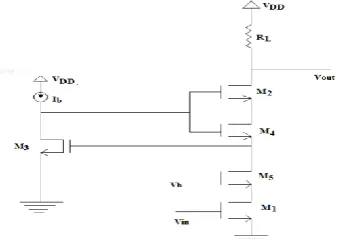
4. SELF CASCODE BASED REGULATED CASCODE AMPLIFIER
The self cascode amplifier has higher cutoff frequency and output impedance due to its shorter channel length. So in conventional regulated cascode amplifier replace transistor M2 by self cascode amplifier to increase the bandwidth. The self cascode based RGC amplifier is shown in Figure 3. The operating principle of self cascode based RGC is approximately similar to conventional RGC amplifier. The transistor M1 will convert the input voltage into drain current Id4. Since in the self cascode amplifier of above circuit, transistor M4 operates in triode region so it works as a resistor. The current Id4will flow through the drain of M2 as Id2and goes to the output terminal Vout. To reduce the channel-length modulation of M1, the respective drain-source voltage must be kept stable. In the regulated cascode, the channel length modulation can be reduced by using feedback loop consisting of an amplifier M3 . In this way, the drain-source voltage of M1 is regulated to a fixed value.
Figure 3. Self cascode based RGC amplifier
Assuming ro1 = ro2 = ro3 = ro and gmiro>>1 (i= 1–4), the transfer function obtained is given by, Where, gm1, gm2
gm3 and gm4 are the transconductance of transistor M1,
M2, M3 and M4, respectively. RL is the load resistance of
the circuit. r0 is the output resistance which is assumed to be the same value for each MOS.
1 2 3 4 2
2 3 4 2 4 3 2 3 4 ( )
(
m m m m o L
V
gs gs m o L
gs m m o L
m m m o
g g g g r R
A s
s C C g r R
sC g g r R
g g g r
(4)
The regulated cascode amplifier provides the large voltage gain and larger output impedance than that of cascode amplifier. To further increase the voltage gain of self cascode based regulated cascode amplifier, a simple self cascode RGC amplifier has been proposed.
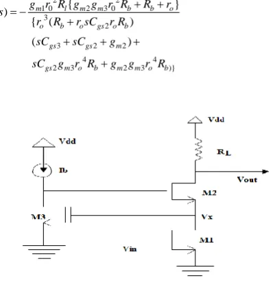
5. SIMPLE SELF CASCODE RGC AMPLIFIER CIRCUIT
The proposed simple self cascode RGC circuit is shown in Figure 4. It consists of a cascode amplifier constructed by transistor M1 and M5 in order to improve the gain, a self cascode amplifier having transistor M2
and M4 and one transistor M3 coupled in feedback to
preserve the constant drain to source voltage of cascode circuit. The feedback mechanism sustains the biasing of self cascode stage and the biasing current for the circuit is taken 10 µA.
The transistor M1 produces a drain current Id1 by converting the input voltage Vininto a current. Since M5 is working as a current buffer, drain current of M5 is equal to Id1. Transistor M1will operate in triode region while M5 will be in saturation region for suitable operation. The self cascode stage in the above circuit is operating in triode region so the output current will be the same as Id1. The transistor M3which is connected as feedback functioning in triode region. It maintains the constant drain to source voltage of cascode transistor and holds the biasing of self cascode amplifier.
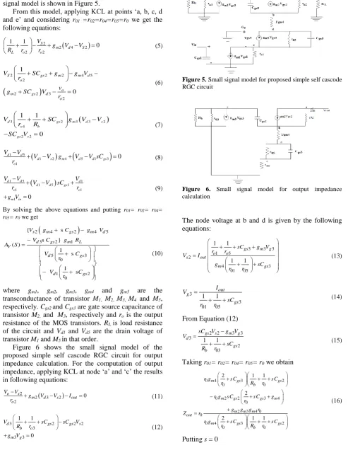
The proposed simple self cascode RGC amplifier small signal model is shown in Figure 5.
From this model, applying KCL at points ‘a, b, c, d and e’ and considering r01 =r02=r04=r05=r0 we get the following equations:
2
2 4 2
2 2
1 1
0 S
m d S
L o o
V
g V V
R r r
(5)
2 2 2 4 5
2
2 2 3
2
1
0
S gs m m d
o
o
m gs d
o
V SC g g V
r
v
g SC V
r (6)
3 2 3 3 2
4
2 2
1 1
0
d gs m d s
o b
gs s
V SC g V V
r R SC V (7)
1 51 2 4 5 1 3
1
0
d d
d s m d d gs
o
V V
V V g V V sC
r
(8)
1 5 1
1 5 3
1 1
1 0
d d d
d d gs
o o
m in
V V V
V V sC
r r g V (9)
By solving the above equations and putting r01= r02= r04= r05= r0 we get
2 4 2 4 5
3 2 1
5 3
0
1 2
0
{ s
s }
1 s ( r 1 r ) s
s m gs m d
d gs m L
d gs
d g
V
s
V g C
A
g V
V C g
S R V C V C (10)
where gm1, gm2, gm3, gm4 and gm5 are the transconductance of transistor M1, M2, M3, M4 and M5, respectively. Cgs2and Cgs3 are gate source capacitance of transistor M2, and M3, respectively and ro is the output resistance of the MOS transistors. RLis load resistance of the circuit and Vd1 and Vd5 are the drain voltage of transistor M1 and M5in that order.
Figure 6 shows the small signal model of the proposed simple self cascode RGC circuit for output impedance calculation. For the computation of output impedance, applying KCL at node ‘a’ and ‘c’ the results in following equations:
2
2 3 2
2
0
o s
m d s out
o
V V
g V V I
r
(11)
3 2 2 2
3 3 3
1 1
0
d gs gs s
b o
m g
V sC sC V
R r g V (12)
Figure 5. Small signal model for proposed simple self cascode RGC circuit
Figure 6. Small signal model for output impedance calculation
The node voltage at b and d is given by the following equations:
3 3 3
1 5 2 4 3 01 05 1 1 1 1
gs m g
o o
s out
m gs
sC g V
r r V I g sC r r (13) 3 3 01 05 1 1 out g gs I V sC r r
(14)
From Equation (12)
2 2 3 3 3
2 03
1 1
gs s m g
d
gs b
sC V g V
V
sC
R r
(15)
Taking r01= r02= r04= r05= r0we obtain
0 4 3 2
0 0
0 2 2 3 4
0 2 3 4 0 0
0 4 3 2
0 0
2 1 1
2
2 1 1
m gs gs
b
m gs gs m
m m m
out
m gs gs
b
r g s C s C
r R r
r g s C s C g
r
g g g r
Z r
r g s C s C
r R r
(16)
2 3 0 0
0 1
1 1
2
m m
out
b g g r
R r
R r
(17)
Bandwidth of the proposed circuit is given by,
1 5
0
3 5 2 1 0
d d
gs d gs d
V V
W
C V C V r
(18)
The expression for bandwidth of the proposed simple self cascode RGC circuit is inversely proportional to r0 and it also depends on the gate source capacitance of the transistor M2 and M3and it increase the bandwidth.
6. SIMULATION AND RESULTS AND ANALYSIS
In the proposed simple self cascode RGC circuit replacing the input transistor M1 by a cascode amplifier
(M1 and M5) in the self cascode based RGC amplifier to
improve the gain. The various amplifiers are constructed and calculated the significant parameters such as voltage gain, output impedance, bandwidth and power dissipation. TANNER EDA tool 12.5 using180 nm technologies have been adopted for designing the amplifiers circuits with the device parameter given in Table 1.
The performances of the amplifiers are investigated under I-V characteristics, DC analysis, AC analysis with varying frequency range of 1 to 10 GHz and transient analysis executed with time interval of 0 to 100 ns.
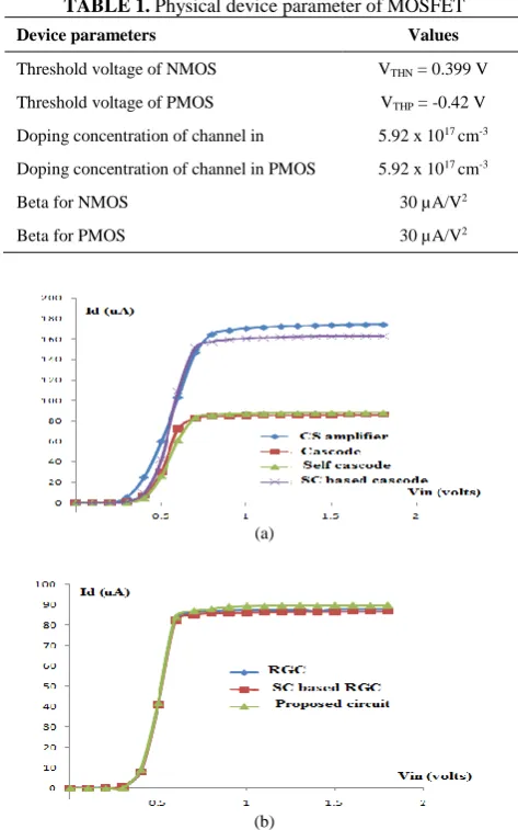
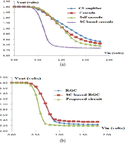
6. 1. Case 1: I-V Characteristics for Different Amplifiers To plot I-V characteristics of various amplifier circuits, the power supply voltage is considered as 1.8 V and the input voltage is varied from 0 to 1.8 V. Figure 7(a) shows the I-V characteristics for common source amplifier, cascode amplifier, self cascode amplifier and self cascode based cascode amplifier. The maximum value of drain current at the output of common source amplifier is 173.88 µA and for self cascode based cascode amplifier it is almost similar which is equal to 162.81 µA. For cascode amplifier and self cascode the value of drain current is approximately the same as 86.11 µA and 87.98 µA, respectively. Figure 7(b) shows the I-V characteristics for RGC, SC based RGC and proposed simple self cascode RGC circuit. From this figure, it can be concluded that the captured value of drain current at the output terminal is approximately the same for all the three amplifiers.
6. 2. Case 2: DC Analysis Figure 8(a) shows the DC transfer characteristics for CS amplifier, cascode amplifier, self cascode amplifier and self cascode based
cascode amplifier. For CS amplifier the output voltage swing is from 1.8 to 0.52 Volts and for cascode amplifier the output voltage swing is varying from 1.8 to 0.45 Volts. The output voltage swing for self cascode amplifier is 1.8 to 0.40 Volts whereas for self cascode based cascode voltage swing is measured as highest from 1.8 to 0.27 Volts. The DC transfer characteristics for RGC, self cascode based RGC and proposed circuit is plotted in Figure 8(b). The output voltage swing for RGC amplifier is varying from 1.8 to 0.23 Volts while for self cascode based RGC is 1.8 to 0.33 Volts that slightly less than RGC. The proposed simple self cascode RGC circuit is facilitated the maximum output voltage swing from 1.8 to 0.19 volt.
6. 3. Case 3: AC Analysis The ac analyses of the various amplifiers are performed for calculating the voltage gain and bandwidth of the circuits.
TABLE 1. Physical device parameter of MOSFET
Device parameters Values
Threshold voltage of NMOS VTHN = 0.399 V
Threshold voltage of PMOS VTHP = -0.42 V
Doping concentration of channel in 5.92 x 1017 cm-3
Doping concentration of channel in PMOS 5.92 x 1017 cm-3
Beta for NMOS 30 µA/V2
Beta for PMOS 30 µA/V2
(a)
(b)
(a)
(b)
Figure 8. (a) DC analysis of CS, Cascode, Self cascode and SC based cascode amplifiers and (b) DC analysis of RGC, Self cascode based RGC and proposed simple self cascode RGC circuit
For the AC analysis, supply voltage 1.5 Volt with the varying frequency ranges from 1 Hz to 10 GHz have been considered. Figure 9(a) shows the gain vs frequency curve for CS amplifier, cascode amplifier, self cascode amplifier and SC based cascode amplifier. The value of voltage gain for CS amplifier is 28.12 dB whereas for the cascode amplifier is equal to 36.58 dB. For self cascode amplifier gain is 38.32 dB and SC based cascode amplifier is 39.63 dB that illustrate an increase in the voltage gain. Figure 9(b) shows the gain vs frequency curve for RGC, SC based RGC and proposed simple self cascode RGC circuits. The calculated voltage gain for RGC amplifier is 48 dB and self cascode based RGC gain is almost same as 48.29 dB. For the proposed simple self cascode RGC circuit, the voltage gain is 58.37 dB that proofed the voltage gain is increased. The bandwidth of the proposed simple self cascode RGC circuit is measured as 45.85 MHz.
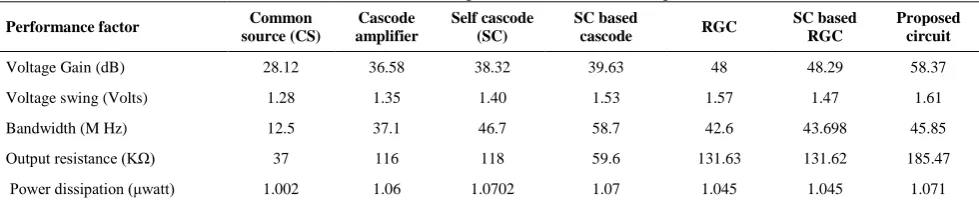
6. 4. Case 4: Transient Analysis From the transient analysis, average power consumption is calculated for the various amplifier circuits. For this analysis, the input signal is considered as a pulse of magnitude 1.5 V. Figure 10(a) shows the transient analysis from the variation of input and output voltages (Volts) with respect to time (ns) for common source amplifier. The power dissipation of the common source amplifier is 1.002 µwatt at 1ns.
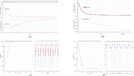
Figure 10(b) shows the transient analysis of the cascode amplifier and it captures the power dissipation 1.06 µWatt. Figures 10(c) and 10(d) show transient analysis for self cascode amplifier and self cascode based cascode amplifier. The calculated value of power dissipation for self cascode amplifier is 2.07 µWatt whereas for self cascode based cascode amplifier is 1.07 µWatt calculated at 1 ns. Figure 10(e) shows the variation of input and output voltage with respect to time for RGC amplifier. The power dissipation of the RGC amplifier is 1.045 µWatt at 1 ns, which is comparatively less than common source and cascode amplifier. Figure 10(f) shows the transient analysis of self cascode based RGC amplifier and power dissipation for this circuit is 1.045 µWatt which is same as RGC amplifier but less than common source and cascode amplifier. Figure 11 shows the slew rate and noise analysis for regulated cascode amplifier and proposed simple self cascode RGC circuit.
The performances of the various amplifiers have been investigated with different parameters that are shown in Table 2. For common source (CS) amplifier voltage gain is obtained 28.12 dB, output voltage swing 1.28 volts, output impedance 37 KΩ with bandwidth of 12.5 MHz and power dissipation is approximately 1 µWatt.
(a)
(b)
(a) (b)
(c) (d)
(e) (f)
Figure 10. Transient analysis of (a) common source amplifier, (b) cascode amplifier, (c) self cascode amplifier, (d) self cascode based cascode amplifier, (e) RGC amplifier and (f) self cascode based RGC amplifier
(a) (b)
(c) (d)
TABLE 2. Value of various parameters for different amplifiers
Performance factor Common
source (CS)
Cascode amplifier
Self cascode (SC)
SC based
cascode RGC
SC based RGC
Proposed circuit
Voltage Gain (dB) 28.12 36.58 38.32 39.63 48 48.29 58.37
Voltage swing (Volts) 1.28 1.35 1.40 1.53 1.57 1.47 1.61
Bandwidth (M Hz) 12.5 37.1 46.7 58.7 42.6 43.698 45.85
Output resistance (KΩ) 37 116 118 59.6 131.63 131.62 185.47
Power dissipation (μwatt) 1.002 1.06 1.0702 1.07 1.045 1.045 1.071
Using cascode amplifier gain increases to 36.58 dB with bandwidth of 37.1 MHz. the power dissipation for cascode amplifier is the same as that of CS amplifier whereas output resistance and output voltage swing increases to 116 KΩ and 1.35 volts, respectively. In self cascode amplifier, the voltage swing has increased up to 1.40 volts while all other parameters are almost of same value as cascode amplifier. Output voltage swing and voltage gain are increased in RGC and self cascode based RGC circuits up to a value of 48 dB, 1.57 volts and 48.29 dB, 1.47 volts, respectively.
The output impedance and bandwidth for RGC and self cascode based RGC raised to 131.63 K Ω, 42.6 MHz and 131.62 K Ω, 43.69 MHz, respectively. Power dissipation of the proposed simple self cascode RGC circuit is 1.071 µWatt and voltage gain is 58.37 dB which is approx 10 dB more than the RGC amplifier. The bandwidth of the proposed circuit is 45.85 dB which is approximately same as self cascode based RGC amplifier. The output impedance is 185.47 KΩ and output voltage swing 1.61 volts. The proposed circuit voltage gain is enhanced and also increases bandwidth compared to other amplifiers.
7. CONCLUSION
Cascode structured amplifier has been employed in various low voltage applications. It provides higher output impedance and reduces the effect of miller capacitance of the amplifier. The proposed simple self cascode RGC circuit consists of a self casocode amplifier and the input transistor of RGC amplifier is replaced by cascode amplifier to increase the gain. The self cascode amplifier is used to enhance the output impedance and bandwidth of RGC amplifier and one MOS transistor is connected in feedback to maintain the constant drain to source voltage of cascode circuit. While designing the low power amplifier circuit, several factors are taken into consideration such as power supply, input voltage, biasing current and power dissipation. The performances of the various amplifiers have been analyzed and with different parameters voltage gain, output voltage swing, output impedance,
bandwidth and power dissipation. From the investigation, the proposed simple self cascode RGC amplifier voltage gain is enhanced. It also increases output impedance and bandwidth compared to other amplifiers.
8. REFERENCES
1. Zhao, X., Zhang, Q., Wang, Y. and Deng, M., “Transconductance and slew rate improvement technique for current recycling folded cascode amplifier”, AEU -
International Journal of Electronics and Communications,
Vol. 70, No. 3, (2016), 326–330.
2 Zhao, C., Liu, J., Shen, F. and Yi, Y., “Low power CMOS power amplifier design for RFID and the Internet of Things”,
Computers & Electrical Engineering, Vol. 52, (2016), 157–
170.
3. Zhao, X., Fang, H., Ling, T. and Xu, J., “Low-voltage process-insensitive frequency compensation method for two-stage OTA with enhanced DC gain”, AEU - International Journal of
Electronics and Communications, Vol. 69, No. 3, (2015), 685–
690.
4. Wang, J., Zhu, Z., Liu, S. and Ding, R., “A low-noise programmable gain amplifier with fully balanced differential difference amplifier and class-AB output stage”,
Microelectronics Journal, Vol. 64, (2017), 86–91.
5. Comer, D.J., Comer, D.T. and Petrie, C.S., “The utility of the composite cascode in analog CMOS design”, International
Journal of Electronics, Vol. 91, No. 8, (2004), 491–502.
6. Prodanov, V.I. and Green, M.M., “CMOS current mirrors with reduced input and output voltage requirements”, Electronics
Letters, Vol. 32, No. 2, (1996), 104–105.
7. Aghnout, S. and Masoumi, N., “Modeling of Substrate Noise Impact on a Single-Ended Cascode LNA in a Lightly Doped Substrate (RESEARCH NOTE)”, International Journal of
Engineering - Transactions A: Basics, Vol. 23, No. 1, (2009),
23–28.
8. Raj, N., Singh, A.K. and Gupta, A.K., “Low voltage high performance bulk driven quasi-floating gate based self-biased cascode current mirror”, Microelectronics Journal, Vol. 52, (2016), 124–133.
9. Sedaghat, S.B., Karimi, G. and Banitalebi, R., “A Low Voltage Full-band Folded Cascoded UWB LNA with Feedback Topology”, International Journal of Engineering -
Transactions A: Basics, Vol. 28, No. 1, (2014), 66–73.
10. Kaur, J., Prakash, N. and Rajput, S.S., “A Low Voltage High Performance Self Cascode Current Mirror”, International
Journal of Electronics and communication Engineering, Vol.
11. Galal, A.I.A., Pokharel, R., Kanaya, H. and Yoshida, K., “High linearity technique for ultra-wideband low noise amplifier in 0.18 μm CMOS technology”, AEU - International Journal of
Electronics and Communications, Vol. 66, No. 1, (2012), 12–
17.
12. Chen, C. L., Hsieh, W. L., Lai, W. J., Chen, K. H. and Wang, C. S., “A high-speed and precise current sensing circuit with bulk control (CCB) technique”, 15th IEEE International Conference
on Electronics, Circuits and Systems, IEEE, (2008), 283–287. 13. Kundra, S., Soni, P. and Kundra, A., “Low power folded
cascode OTA”, International Journal of VLSI design &
Communication Systems, Vol. 3, No. 1, (2012), 127–136.
14. Shekhar, S., Walling, J.S. and Allstot, D.J., “Bandwidth Extension Techniques for CMOS Amplifiers”, IEEE Journal of
Solid-State Circuits, Vol. 41, No. 11, (2006), 2424–2439.
Study and Analysis of A Simple Self Cascode Regulated Cascode Amplifier
P. Karuppanan, K. Anuradha
Department of Electronics and Communication Engineering, Motilal Nehru National Institute of Technology Allahabad, India
P A P E R I N F O
Paper history:
Received 29 July 2017
Received in revised form 26 April 2018 Accepted 26 April 2018
Keywords: Self Cascode Regulated Cascode
Self Cascode Based Regulated Cascode Simple Self Cascode Regulated Cascode
هدیکچ
یلپمآ یدنبرکیپ کی ،هلاقم نیا رد ریاف
RGC
هپ و دوس شیازفا یارب هداس رتویپماکدوخ .تسا هدش داهنشیپ دناب یان
یلپمآ م تیفرظ دووکساک ریاف یم فذح یجورخ و یدورو نیب ار زلی
،لااب سنادپما و دنک لااب یدورو
ر لااب دناب یانهپ و ا
یم لیهست تیوقت ،لاح نیا اب .دنک ًاتبسن هیذغت عبنم ژاتلو هب زاین نودکاوک هدننک
ناسون و دراد بسانم درکلمع یارب لااب
ژاتلو اب ار یجورخ ژاتلو
overdrive
یم شهاک یلپمآ اب لئاسم نیا .دهد ریاف
RGC
یم هبلغ رتویپماکدوخ رب ینتبم ؛دنک
ب هجوت اب مک دناب یانهپ رگا یتح یجورخ سنادپما و دناب یانهپ .دشاب نییاپ سناکرف رد نآ بطق کی روضح ه
RGC
ا هتفای شیازفا جوم لوط میسقت ناربج شور زا هدافتسا اب یلومعم تیوقت یلک درکلمع دوبهب یارب .تس
کی ،هدننک
RGC
دپما نایب .تسا هدش یفرعم یفاضا لعفنم رصانع زا هدافتسا نودب هداس تکساک دوخ ازفا سنا
یارب سنادپما و شی
تیوقت حم رادقم .تسا هدش قتشم کچوک لانگیس لیلحت زا هدافتسا اب یداهنشیپ هدننک رادم یارب ژاتلو زا هدش هبسا
شیپ هدش ینیب
dB
73 / 85 زا رتشیب هک تسا
RGC
یداهنشیپ رادم تردق نداد تسد زا .تسا وکساک دوخ رب ینتبم
73 / 1 اب و تسا تاواگم
CS
،
cascode
،
selfcascode
و
cascodebasedSC
،
RGC
،
SC
تیوقت هدننک یاه
RGC