Adv. Radio Sci., 9, 383–389, 2011 www.adv-radio-sci.net/9/383/2011/ doi:10.5194/ars-9-383-2011
© Author(s) 2011. CC Attribution 3.0 License.
Advances in
Radio Science
Advanced parametrical modelling of 24 GHz radar sensor IC
packaging components
R. Kazemzadeh1, W. John2, J. Wellmann1, U. B. Bala1, and A. Thiede1
1University of Paderborn (HFE), Paderborn, Germany
2Leibniz University Hannover (TET), Hannover/SIL R+D, Paderborn, Germany
Abstract. This paper deals with the development of an
ad-vanced parametrical modelling concept for packaging com-ponents of a 24 GHz radar sensor IC used in automotive driver assistance systems. For fast and efficient design of packages for system-in-package modules (SiP), a simplified model for the description of parasitic electromagnetic effects within the package is desirable, as 3-D field computation be-comes inefficient due to the high density of conductive ele-ments of the various signal paths in the package. By using lumped element models for the characterization of the con-ductive components, a fast indication of the design’s signal-quality can be gained, but so far does not offer enough flex-ibility to cover the whole range of geometric arrangements of signal paths in a contemporary package. This work pur-sues to meet the challenge of developing a flexible and fast package modelling concept by defining parametric lumped-element models for all basic signal path components, e.g. bond wires, vias, strip lines, bumps and balls.
1 Introduction
To obtain the lumped element models for the parametric modelling concept, the parametric simulations of the con-sidered structures are first carried out with 3-D field solvers (like EMPIRE, 2009), where the parameter typically is a ge-ometric quantity, like length, height, diameter, thickness or distance of the structures. Then, the simulation results are used to obtain the lumped-element description of the conduc-tive structure. Section 2 examines the feasibility of the pur-sued parametric modelling concept by reassembling signal path structures from the parametric lumped element charac-terizations of the basic conductive components and
compar-Correspondence to: W. John
ing the results of the lumped element signal path models to those of the 3-D field calculations. Section 3 deals with the modelling of parametric ball structures. Section 4 addresses the parametric modelling of bond wire structures with focus on different numerical tools to minimize the effect of their specific behaviour.
2 Parametric modelling of vertical interconnect structures
This section addresses the issue whether it is possible to char-acterize the electromagnetic behaviour of a package signal path by interconnection of RLC models of the basic signal path elements, like vias, bond wires, balls, strip lines or com-binations of these. To verify the feasibility of the pursued parametrical modelling concept, as a first step only the via inductance is being focused on, neglecting the coupling ca-pacitance between the via-body and the P/G-planes accord-ing to the equivalent circuit model of a via in Fig. 1.
The examination of via-configurations in conjunction with signal lines shows that the characteristic behaviour of such a configuration, e.g. the impedance characteristic, cannot be approximated by simple interconnection of the RLC models. For instance, the characteristic of a via with a via length of lViaBody=100 µm and micro strip length of lMicrostrip= 50 µm, secluding at the upper and lower via pad, cannot simply be characterized by an interconnection of the RLC models of e.g. a via with lViaBody=50 µm in conjunction with a micro strip oflMicrostrip=50 µm and another via with
384 R. Kazemzadeh et al.: Advanced parametrical modelling of 24 GHz radar sensor IC packaging components
1
R
ViaBodyGND
GND
C
ViaGNDC
ViaGNDL
ViaBodyAdvanced Parametrical Modelling of 24 GHz
Radar Sensor IC Packaging Components
R. Kazemzadeh
#
, J. Wellmann
#
, U.B. Bala
#
, W. John
*
, A. Thiede
#
#
University of Paderborn (HFE) - Paderborn
*
Leibniz University Hannover (TET) - Hannover/SIL R+D - Paderborn
Correspondence to Dr.-Ing. W. John - [email protected]
Abstract.
This paper deals with the
development of an advanced parametrical
modelling
concept
for
packaging
components of a 24 GHz radar sensor IC
used in automotive driver assistance
systems. For fast and efficient design of
packages for system-in-package modules
(SiP), a simplified model for the
description of parasitic electromagnetic
effects within the package is desirable, as
3D field computation becomes inefficient
due to the high density of conductive
elements of the various signal paths in the
package. By using lumped element models
for the characterization of the conductive
components, a fast indication of the
design’s signal-quality can be gained, but
so far does not offer enough flexibility to
cover the whole range of geometric
arrangements of signal paths in a
contemporary package. This work pursues
to meet the challenge of developing a
flexible and fast package modelling
concept by defining
parametric
lumped-element models for all basic signal path
components, e.g. bond wires, vias, strip
lines, bumps and balls.
1 Introduction
To obtain the lumped element models for
the parametric modelling concept, the
parametric simulations of the considered
structures are first carried out with 3D field
solvers (like [5]), where the parameter
typically is a geometric quantity, like
length, height, diameter, thickness or
distance of the structures. Then, the
simulation results are used to obtain the
lumped-element
description
of
the
conductive structure. Section 2 examines
the feasibility of the pursued parametric
modelling concept by reassembling signal
path structures from the parametric lumped
element characterizations of the basic
conductive components and comparing the
results of the lumped element signal path
models to those of the 3D field
calculations. Section 3 deals with the
modelling of parametric ball structures.
Section 4 addresses the parametric
modelling of bond wire structures with
focus on different numerical tools to
minimize the effect of their specific
behaviour.
2 Parametric Modelling of Vertical
Interconnect Structures
Fig. 1
Equivalent circuit model of a via
This section addresses the issue whether it
is
possible
to
characterize
the
Fig. 1. Equivalent circuit model of a via.
electromagnetic behaviour of a package
signal path by interconnection of RLC
models of the basic signal path elements,
like vias, bond wires, balls, strip lines or
combinations of these. To verify the
feasibility of the pursued parametrical
modelling concept, as a first step only the
via inductance is being focused on,
neglecting
the
coupling
capacitance
between the via-body and the P/G-planes
according to the equivalent circuit model
of a via in fig.1.
The examination of via-configurations in
conjunction with signal lines shows that
the characteristic behaviour of such a
configuration,
e.g.
the
impedance
characteristic, cannot be approximated by
simple interconnection of the RLC models.
Fig. 2
Graphical representation of a via
For instance, the characteristic of a via
with a via length of
l
ViaBody= 100 µm and
micro strip length of
l
Microstrip= 50 µm,
secluding at the upper and lower via pad,
cannot simply be characterized by an
interconnection of the RLC models of e.g.
a via with
l
ViaBody= 50 µm in conjunction
with a micro strip of
l
Microstrip= 50 µm and
another via with
l
ViaVody= 50 µm. Hence,
the RLC models of the individual elements
(via, ball, bond wire etc.) are not suitable
as basic models for the pursued modelling
concept, since the occurring effects at the
interfaces of the interconnected elements
are not being regarded. The consideration
of these effects would require modelling
them individually. Here, a different
approach
is
followed
by
using
combinations of the individual signal path
elements as basic RLC models. More
precisely, a via in conjunction with micro
strip lines at its upper and lower pad serves
as
a
basic
model,
allowing
the
consideration of transition effects at the
micro strip/via-pad junction. Using a 3D
FDTD solver for all electromagnetic field
simulations,
a
simple
signal
path
arrangement consisting of three vertically
interconnected vias with micro strip lines
at the very upper and very lower via-pad is
being examined. As can be expected, this
signal path arrangement shows nearly the
same impedance characteristic as a single
via of the same overall via length and
micro strip length. Fig. 3 shows the
inductance
L
SPof the considered signal
path arrangement as a function of its
overall vertical length
l
Vertical.
Fig. 3
Signal path inductance L
SP(vertical
and horizontal signal path length for basis
model (continuous curves)) - three
vertically interconnected vias (dashed) -
signal path arrangement (array of curves)
Here, the inductance of the single vias in
conjunction with signal lines is represented
by
continuous
lines,
whereas
the
inductance of the simple signal path
arrangement of three vertically connected
vias in conjunction with signal lines is
shown by the dashed lines. As the
capacitive via-GND coupling is not
regarded at this stage, the impedance
characteristic can be approximated from
the inductance values displayed in fig. 3,
L
ViaPadD
ViaPadD
ViaBodyD
DrillHoleL
ViaBodyFig. 2. Graphical representation of a via.
signal path elements as basic RLC models. More precisely, a via in conjunction with micro strip lines at its upper and lower pad serves as a basic model, allowing the considera-tion of transiconsidera-tion effects at the micro strip/via-pad juncconsidera-tion. Using a 3-D FDTD solver for all electromagnetic field simu-lations, a simple signal path arrangement consisting of three vertically interconnected vias with micro strip lines at the very upper and very lower via-pad is being examined. As can be expected, this signal path arrangement shows nearly the same impedance characteristic as a single via of the same overall via length and micro strip length. Fig. 3 shows the in-ductanceLSPof the considered signal path arrangement as a
function of its overall vertical lengthlVertical.
Here, the inductance of the single vias in conjunction with signal lines is represented by continuous lines, whereas the inductance of the simple signal path arrangement of three vertically connected vias in conjunction with signal lines is shown by the dashed lines. As the capacitive via-GND
cou-2
electromagnetic behaviour of a package
signal path by interconnection of RLC
models of the basic signal path elements,
like vias, bond wires, balls, strip lines or
combinations of these. To verify the
feasibility of the pursued parametrical
modelling concept, as a first step only the
via inductance is being focused on,
neglecting
the
coupling
capacitance
between the via-body and the P/G-planes
according to the equivalent circuit model
of a via in fig.1.
The examination of via-configurations in
conjunction with signal lines shows that
the characteristic behaviour of such a
configuration,
e.g.
the
impedance
characteristic, cannot be approximated by
simple interconnection of the RLC models.
Fig. 2
Graphical representation of a via
For instance, the characteristic of a via
with a via length of
l
ViaBody= 100 µm and
micro strip length of
l
Microstrip= 50 µm,
secluding at the upper and lower via pad,
cannot simply be characterized by an
interconnection of the RLC models of e.g.
a via with
l
ViaBody= 50 µm in conjunction
with a micro strip of
l
Microstrip= 50 µm and
another via with
l
ViaVody= 50 µm. Hence,
the RLC models of the individual elements
(via, ball, bond wire etc.) are not suitable
as basic models for the pursued modelling
concept, since the occurring effects at the
interfaces of the interconnected elements
are not being regarded. The consideration
of these effects would require modelling
them individually. Here, a different
approach
is
followed
by
using
combinations of the individual signal path
elements as basic RLC models. More
precisely, a via in conjunction with micro
strip lines at its upper and lower pad serves
as
a
basic
model,
allowing
the
consideration of transition effects at the
micro strip/via-pad junction. Using a 3D
FDTD solver for all electromagnetic field
simulations,
a
simple
signal
path
arrangement consisting of three vertically
interconnected vias with micro strip lines
at the very upper and very lower via-pad is
being examined. As can be expected, this
signal path arrangement shows nearly the
same impedance characteristic as a single
via of the same overall via length and
micro strip length. Fig. 3 shows the
inductance
L
SPof the considered signal
path arrangement as a function of its
overall vertical length
l
Vertical.
Fig. 3
Signal path inductance L
SP(vertical
and horizontal signal path length for basis
model (continuous curves)) - three
vertically interconnected vias (dashed) -
signal path arrangement (array of curves)
Here, the inductance of the single vias in
conjunction with signal lines is represented
by
continuous
lines,
whereas
the
inductance of the simple signal path
arrangement of three vertically connected
vias in conjunction with signal lines is
shown by the dashed lines. As the
capacitive via-GND coupling is not
regarded at this stage, the impedance
characteristic can be approximated from
the inductance values displayed in fig. 3,
L
ViaPadD
ViaPadD
ViaBodyD
DrillHoleL
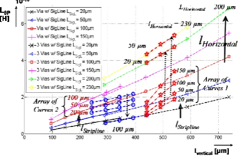
ViaBodyFig. 3. Signal path inductanceLSP (vertical and horizontal signal path length for basis model (continuous curves)) – three vertically interconnected vias (dashed) – signal path arrangement (array of curves).
pling is not regarded at this stage, the impedance character-istic can be approximated from the inductance values dis-played in Fig. 3, since the loss resistance of the considered arrangements is negligible. The second parameter, besides the vertical overall lengthlVertical of the signal path arrange-ments, is the horizontal signal line lengthlHorizontal. Ascend-ing in the direction of the ordinate, each curve represents an arrangement with a constant signal line length, as indicated in the legend of Fig. 3 and as assigned at the array of curves in the same figure. The inductance of the arrangements of vias grows nearly linearly with increasing via length. Further-more, the inductance increases with the signal line length. Comparing the dashed curves for the three via arrangement, an increase in signal line length involves an increase of the gradient for the respective curve. Since the inductance in-creases nearly linearly with the via length and the gradient of the curves rises nearly linearly with the signal line length, every point in the considered space or, respectively, within the considered geometric domain for the signal path arrange-ments can be approximated by means of simple algorithms.
To further verify the parametric modelling concept, in a next step a benchmark signal path example is established to see if it is possible to approximate its impedance character-istic by interconnection of variations of the basic via/signal line model.
Figure 4a–d shows the signal path example consisting of three vias, two of which are positioned above each other, with the third via positioned on the level of the gap be-tween the two vias, but laterally displaced. The three vias are interconnected with strip lines according to Fig. 4. Four geometric parameters are analyzed: The length of the strip lines lStripline between the middle via and the upper/lower via (Fig. 4a), the length of the micro striplMicrostrip at the upper/lower via (Fig. 4b), the length of the middle via-bodylMidVia(Fig. 4c) and the length of the lower via-body
R. Kazemzadeh et al.: Advanced parametrical modelling of 24 GHz radar sensor IC packaging components 385
3
since the loss resistance of the considered
arrangements is negligible. The second
parameter, besides the vertical overall
length
l
Verticalof
the
signal
path
arrangements, is the horizontal signal line
length
l
Horizontal. Ascending in the direction
of the ordinate, each curve represents an
arrangement with a constant signal line
length, as indicated in the legend of fig. 3
and as assigned at the array of curves in the
same figure. The inductance of the
arrangements of vias grows nearly linearly
with increasing via length. Furthermore,
the inductance increases with the signal
line length. Comparing the dashed curves
for the three via arrangement, an increase
in signal line length involves an increase of
the gradient for the respective curve. Since
the inductance increases nearly linearly
with the via length and the gradient of the
curves rises nearly linearly with the signal
line length, every point in the considered
space
or,
respectively,
within
the
considered geometric domain for the signal
path arrangements can be approximated by
means of simple algorithms.
To further verify the parametric modelling
concept, in a next step a benchmark signal
path example is established to see if it is
possible to approximate its impedance
characteristic
by
interconnection
of
variations of the basic via/signal line
model.
Fig. 4
Investigated signal path arrangement
with examined parameters: (a) strip line
length
l
Stripline- (b) micro strip length
l
Microstrip- (c) middle via-body length
l
MidVia- (d) lower via body length
l
LowViaFig. 4 a-d shows the signal path example
consisting of three vias, two of which are
positioned above each other, with the third
via positioned on the level of the gap
between the two vias, but laterally
displaced.
The
three
vias
are
interconnected with strip lines according to
fig. 4. Four geometric parameters are
analyzed: The length of the strip lines
l
Striplinebetween the middle via and the
upper/lower via (fig. 4 a), the length of the
micro strip
l
Microstripat the upper/lower via
(fig. 4 b), the length of the middle via-body
l
MidVia(fig. 4 c) and the length of the lower
via-body
l
LowVia(fig. 4 d). The range of
variation of the geometric parameters for
the signal path arrangement is listed in
table 1, in addition to the other via and
signal line parameters. An illustration of
the via parameters is given in fig. 2. First,
the variation of the middle via-body length
l
Microstripin conjunction with the strip line
length
l
Striplinewas analyzed (fig. 4 a/c),
where the length of the upper and lower
via-body is
l
UpVia,l
LowVia= const.
= 50 µm
and the length of the micro strip is
l
Microstrip= const.
= 20 µm.
The results, displayed by the
array of
curves 1
, were displaced 200 units in the
direction of the abscissa to not overlay
with the
array of curves 2
in fig. 3. It is
apparent that the curves of
array 1
have a
higher gradient compared to the rest of the
curves. As mentioned earlier, the gradient
of a curve at a certain via length is
determined by the length of the signal lines
connected to the via. Although the length
of the micro strip and the strip line is
l
Stripline- l
Microstrip= 20 µm for the under
most curve of the
array 1
, the gradient is
evidently higher than the gradients of the
curves for the basic models with the same
or even higher signal line lengths. Moving
the two under most curves of
array 1
onto
the curves for the three vertically
interconnected vias in conjunction with
signal line lengths
l
Horizontal= 200 µm and
l
Horizontal= 230 µm shows the same
gradients for each pair of curves, as
l
Striplinel
Microstripl
LowVial
MidVia(c) (a)
(d) (b)
Fig. 4. Investigated signal path arrangement with examined parame-ters: (a) strip line lengthlStripline– (b) micro strip lengthlMicrostrip – (c) middle via-body lengthlMidVia– (d) lower via body length
lLowVia.
lLowVia (Fig. 4d). The range of variation of the geometric parameters for the signal path arrangement is listed in Ta-ble 1, in addition to the other via and signal line parame-ters. An illustration of the via parameters is given in Fig. 2. First, the variation of the middle via-body lengthlMicrostripin conjunction with the strip line lengthlStripline was analyzed (Fig. 4a/c), where the length of the upper and lower via-body islUpVia,lLowVia=const.=50µm and the length of the micro strip islMicrostrip=const.=20 µm.
The results, displayed by the array of curves 1, were dis-placed 200 units in the direction of the abscissa to not over-lay with the array of curves 2 in Fig. 3. It is apparent that the curves of array 1 have a higher gradient compared to the rest of the curves. As mentioned earlier, the gradient of a curve at a certain via length is determined by the length of the signal lines connected to the via. Although the length of the mi-cro strip and the strip line islStripline−lMicrostrip=20µm for the under most curve of the array 1, the gradient is evidently higher than the gradients of the curves for the basic models with the same or even higher signal line lengths. Moving the two under most curves of array 1 onto the curves for the three vertically interconnected vias in conjunction with sig-nal line lengthslHorizontal=200 µm andlHorizontal=230 µm shows the same gradients for each pair of curves, as delin-eated in Fig. 3. Thus, the considered signal path arrange-ment behaves like a basic model with considerably longer signal lines. Comparing the signal path arrangement to the basic model of the same length, the former possesses addi-tional horizontal conductors, which are the lower via pad of the upper via and the upper via pad of the displaced via (or, the lower via pad of the displaced via and the upper via pad of the lower via, respectively) (Fig. 4).
Adding the length of these additional horizontal conduc-tors to the overall signal line length of the signal path ar-rangement, we approximately obtain the signal line length of the basis model with the same gradient as the signal path
Table 1. Parameters of calculated structures.
Characteristic (all Models) Value Unit
Height of signal lines/via pads 23 µm
Width of signal lines 65 µm
Diameter of via-padsdViaPad 142 µm Diameter of via-bodydViaBody 96 µm Diameter of drill holedDrillHole 50 µm Dielectric constant of substrate materialεr 3.5 – Basic Model and Three Vertical Vias Model
Vertical lengthlVertical 96–738 µm Horizontal lengthlHorizontal 20–230 µm Signal Path Arrangement
Middle via-body lengthlMidVia 50–150 µm Up/low via-body length lUpVia−lLowVia 50–150 µm Overall vertical lengthlVertical 242–392 µm Micro strip lengthlMicrostrip 20–150 µm Strip line lengthlStripline 20–150 µm
arrangement, which explains the agreement of the gradients of the curves. Thus, it is possible to approximate the char-acteristic of the signal path arrangement for the parameters
lStripline andlMidViaby means of the basic model. Next, the variation of the lower via-body lengthlLowViain conjunction with the strip line lengthlStriplinewas analyzed (Fig. 4 a/d), where the length of the upper and middle via-body islUpVia andlMidVia=const.=50 µm and the length of the micro strip islMicrostrip=const.=20 µm. The results are displayed by the array of curves 2 in Fig. 3. Here, it stand out that the gra-dients of the curves of array 2 all have the same gradient and that the variation of the strip line lengthlStriplinehas no effect on the gradient, in contrast to the preceding examination of the strip line lengthlStripline in conjunction with the middle via-body length lMidVia. The gradient of the curves is de-termined by the length of the micro striplMicrostrip=const.= 20 µm, independent of the strip line lengthlStripline,which
386 R. Kazemzadeh et al.: Advanced parametrical modelling of 24 GHz radar sensor IC packaging components
packages requires an appropriate way of
modelling.
Regarding the ball geometry, tinned bumps
of pure solder/tin compounds will form a
spherical body after soldering, depending
on the amount of material and the height of
the connection [1].
Table 2
Parameters of calculated structures
Characteristic
(all Models)
Value
Unit
Diameter
d
(Ball)
30 - 480
µ m
Diameter (Pad)
0.8*d
µ m
Height (Pad)
24
µ m
Distance
D
(between
Balls)
200-1600
µ m
Relative permittivity of
substrate/underfill
material
ε
r2.0/3.5/
11.9
--
Conductivity of ball
material
s
rTin
Gold
Copper
8.67*10^6
4.1*10^7
5.8*10^7
1/(Ohm
*m)
In this work, a simplified geometry was
inspected to reduce the number of
parameters for the parametrical lumped
element model to the overall diameter of
the ball. The angles of the cutting-planes
are kept constant, giving a diameter of the
upper and lower pads relative to the balls
diameter.
Different parameters will be used for
modelling: The diameter
d
of the ball, the
distance
D
between two balls,
ε
r
of the
surrounding material and the conductivity
σ
r
of the ball’s material. The dominant
non-resistive elements are the inductance
of the single ball and the
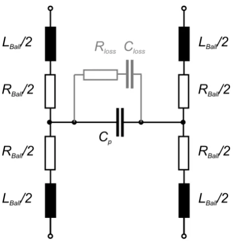
coupling-capacitance between two balls (fig. 5). For
better symmetry, the ball-inductance is
splitted in half, so the coupling-network
between several bumps can be connected
without any vertical mismatch giving a
symmetrical
model.
The
inter-bump
coupling-network includes, apart from the
coupling-capacitance
C
p
,
additional
elements to model resistive and dielectric
losses.
Fig. 5
Equivalent circuit model of two
balls and capacitive coupling
As shown in table 3, the parameterization
of the inductance between ball and
diameter is linear [2].
Table 3
Inductance of a single ball
Ball
Diameter
d
Field
Computation
Parameterization
30 µm
59.5 pH
60 pH
60 µm
65.9 pH
66 pH
90 µm
71.9 pH
72.4 pH
120 µm
77.9 pH
78.3 pH
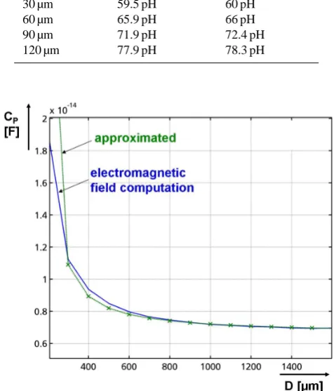
The coupling capacitance
C
p
between two
balls (see fig. 6) dominates the magnetic
coupling factor [3]. It should be noted that
the distance between two balls is measured
between the ball’s central points, so D = d
would mean a direct contact between the
two balls, and an infinity capacitance for
D/d » 0. As shown in fig. 7, the
capacitance converges to a 1/D-behaviour.
For getting an approximation for close ball
distances it is necessary to use the relative
ball distance between central points). The
size of the coupling capacity
C
p
can be
approximated as
1 2
( , ,
)
p r r o
k D
k
C D d
d
D
d
ε
≈
ε ε
+
−
(1)
where
D
is the distance between two balls,
d
the diameter of each ball
,
ε
r
the dielectric
Fig. 5. Equivalent circuit model of two balls and capacitivecou-pling.
can be approximated by a basis model oflVertical= 242 µm andlHorizontal=20 µm in conjunction with a basis model of
lVertical=50 µm andlHorizontal=200 µm.
3 Parametric modelling of ball-structures
The use of spherical ball- or bump-structures for intercon-nections between die and interposer (FlipChip/SIP) or BGA packages requires an appropriate way of modelling.
Regarding the ball geometry, tinned bumps of pure sol-der/tin compounds will form a spherical body after solder-ing, depending on the amount of material and the height of the connection (Hussein, 1996).
In this work, a simplified geometry was inspected to re-duce the number of parameters for the parametrical lumped element model to the overall diameter of the ball. The angles of the cutting-planes are kept constant, giving a diameter of the upper and lower pads relative to the balls diameter.
Different parameters will be used for modelling: The di-ameterd of the ball, the distanceDbetween two balls,εr of
the surrounding material and the conductivityσrof the ball’s
material. The dominant non-resistive elements are the induc-tance of the single ball and the coupling-capaciinduc-tance between two balls (Fig. 5). For better symmetry, the ball-inductance is splitted in half, so the coupling-network between several bumps can be connected without any vertical mismatch giv-ing a symmetrical model. The inter-bump couplgiv-ing-network includes, apart from the coupling-capacitanceCp, additional
elements to model resistive and dielectric losses.
Fig. 6. Ball to ball coupling capacityCP;εr=1.
As shown in Table 3, the parameterization of the induc-tance between ball and diameter is linear (Ndip, 2003).
The coupling capacitance Cp between two balls (see
Fig. 6) dominates the magnetic coupling factor (Ahn, 2000). It should be noted that the distance between two balls is mea-sured between the ball’s central points, soD=dwould mean a direct contact between the two balls, and an infinity ca-pacitance forD/d0. As shown in Fig. 7, the capacitance converges to a 1/D-behaviour. For getting an approximation for close ball distances it is necessary to use the relative ball distance between central points). The size of the coupling capacityCpcan be approximated as
Cp(D,d,εr)≈εrεod2
k1D+k2
D−d (1)
whereDis the distance between two balls,εr the dielectric
constant of the underfill, andk1≈2.29×10⁸,k2≈ −2.32× 10⁶are fitting parameters.
The dielectric losses of the underfill-material are not part of this parametric model, as no major influence was observed for the inspected materials (Polyimide/Epoxy/Polyclad) in the targeted frequency range up to 30 GHz.
For precise modelling of the dielectric losses for higher frequencies or different materials, additional R and RC-Networks can be connected in parallel to the coupling ca-pacitanceCp.
4 Parametric modelling of bond wire
This section deals with the parametrical modelling of bond wires. The bond wires will be parameterized by varying their length and the distance between two bond wires. In the present model, JEDEC4 bond wires are being consid-ered (Fig. 8), where the height of each bond wire is 200 µm and consists of PEC (Perfectly Electrically Conducting) ma-terial. The bond wire radius is 12.5 µm. The substrate is
R. Kazemzadeh et al.: Advanced parametrical modelling of 24 GHz radar sensor IC packaging components 387
Table 2. Parameters of calculated structures.
Characteristic (all Models) Value Unit
Diameterd(Ball) 30–480 µm
Diameter (Pad) 0.8×d µm
Height (Pad) 24 µm
DistanceD(between Balls) 200–1600 µm
Relative permittivity of substrate/underfill materialεr 2.0/3.5/11.9 –
Conductivity of ball materialsr Tin Gold Copper 8.67×1064.1×1075.8×107 1/(Ohm×m)
Table 3. Inductance of a single ball.
BallDiameterd FieldComputation Parameterization
30 µm 59.5 pH 60 pH
60 µm 65.9 pH 66 pH
90 µm 71.9 pH 72.4 pH
120 µm 77.9 pH 78.3 pH
Fig. 7. Coupling capacityCp(ball distanceD;εr=1;d=180 µm.
considered as Silicon (loss free) and the size of each pad is 250 µm×250 µm×15 µm.
First of all, a parameterization of the bond wire will be carried out by variation of its length. In order to achieve this, S-parameters are being computed using the 3-D field calcu-lator CST Microwave Studio. The equivalent circuit model of a single bond wire is shown in Fig. 9. Since PEC ma-terial is considered, there will be no resistance. The pad to GND capacitances are labelledC10andC20 and the capaci-tance between the pads is labelledC12. The bond wire will be represented as an inductance which is divided into two parts
Fig. 8. 3-D model of single bond wire.
Fig. 9. Equivalent circuit model of a single bond wire.
L11andL22, and C0represents the capacitance between the bond wire and the GND. Since the result is renormalized with 50 Ohm resistance, two ports with the same resistance are added at the two ends. The values of these parameters are being obtained using Ansoft Q3-D for the length variation of 400 µm to 2000 µm with a step size of 400 µm. The pad to GND capacitance remains constant,C10=C20=108.4 fF. The results of the other parameters are shown in Table 4.
388 R. Kazemzadeh et al.: Advanced parametrical modelling of 24 GHz radar sensor IC packaging components
Table 4. Different parameters of single bond wire.
Bond Wire Length [µm] Pad CapacitanceC12[fF] Bond Wire Inductance [pH] Bond Wire CapacitanceC0[fF]
400 2.22 0.3297 12.89
800 0.0862 0.6539 20.21
1200 0.0326 1.086 25.17
1600 0.0178 1.39 35.44
2000 0.0112 1.79 43.41
Fig. 10. Comparison of S parameters of a single bond wire with varying length.
System). The comparison of the 3-D simulator results with the circuit model results is shown in Fig. 10. The 3-D sim-ulator results coincide well with the equivalent circuit model results. Reasons for deviations are caused by the different numerical algorithms and different meshing of the various simulation tools. Next two bond wires will be parameterized by varying the distance between them. The distance is varied from 300 µm to 700 µm with a step size of 100 µm. The 3-D field calculations were performed using ANSOFT HFSS. Since differential ports are being used, odd modes arise be-tween the two bond wires.
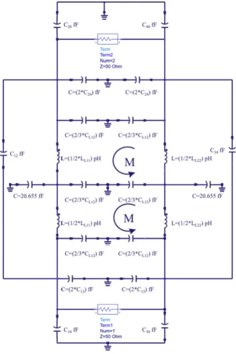
In order to take this effect into account, some modifica-tions (Pozar, 1998) have to be applied to the equivalent cir-cuit model of the two bond wires (Fig. 12). Due to the odd modes, an E-wall will arise between the two bond wires.
Since the capacitance between the first two pads is C13 due to this odd mode, the capacitance between a pad and the E-wall will be 2C13. This effect has to be taken into account for the capacitance between two bond wires, too. In Fig. 12, this capacitance is separated into three parts, whereas the inductance of the bond wire is separated into two parts. The coupling inductance M between the two bond wires must also be taken into account. The values of these parameters
50 Ohm resistance, two ports with the
same resistance are added at the two ends.
The values of these parameters are being
obtained using Ansoft Q3D for the length
variation of 400
µ
m to 2000
µ
m with a
step size of 400
µ
m. The pad to GND
capacitance remains constant, C
10= C
20=
108.4 fF. The results of the other
parameters are shown in table 4.
Table 4
Different parameters of single
bond wire
Bond Wire
Length [µm]
Pad Capacitance
C12 [fF]
Bond Wire
Inductance [pH]
Bond Wire
Capacitance C0 [fF]
400
2.22
0.3297
12.89
800
0.0862
0.6539
20.21
1200
0.0326
1.086
25.17
1600
0.0178
1.39
35.44
2000
0.0112
1.79
43.41
Using these results, the S parameters of
this equivalent circuit are calculated with
the help of ADS (Advanced Design
System). The comparison of the 3D
simulator results with the circuit model
results is shown in fig. 10. The 3D
simulator results coincide well with the
equivalent circuit model results. Reasons
for deviations are caused by the different
Fig. 10
Comparison of S parameters of a
single bond wire with varying length
numerical
algorithms
and
different
meshing of the various simulation tools.
Next two bond wires will be parameterized
by varying the distance between them. The
distance is varied from 300
µ
m to 700
µ
m
with a step size of 100
µ
m. The 3D field
calculations
were
performed
using
ANSOFT HFSS. Since differential ports
are being used, odd modes arise between
the two bond wires.
Fig. 11
3D Model of two bond wires
In order to take this effect into account,
some modifications [Pozar, 1998] have to
be applied to the equivalent circuit model
of the two bond wires (fig. 12). Due to the
odd modes, an E-wall will arise between
the two bond wires.
Table 5 C
apacitance of two bond wires
Vertical
Distance
[
µ
m]
C
10[fF]
C
13[fF]
C
12[fF]
C
L12[fF]
300
109.16 28.45
9.98
5.51
400
109.16 18.20
9.98
4.71
500
109.16 13.93
9.98
4.17
600
109.16 11.41
9.98
3.75
700
109.16
9.71
9.98
3.41
Since the capacitance between the first two
pads is C
13due to this odd mode, the
capacitance between a pad and the E-wall
will be 2C
13. This effect has to be taken
into account for the capacitance between
two bond wires, too. In fig. 12, this
capacitance is separated into three parts,
whereas the inductance of the bond wire is
separated into two parts. The coupling
inductance M between the two bond wires
must also be taken into account. The
Lumped Port
Bond Wire
Pad 2
Pad 4
Pad 3
Pad 1
Fig. 11. 3-D Model of two bond wires.
Table 5. Capacitance of two bond wires.
Vertical Distance [µm] C10[fF] C13[fF] C12[fF] CL12[fF]
300 109.16 28.45 9.98 5.51
400 109.16 18.20 9.98 4.71
500 109.16 13.93 9.98 4.17
600 109.16 11.41 9.98 3.75
700 109.16 9.71 9.98 3.41
are calculated using ANSOFT Q3-D (Tables 5 and 6). The pad (GND capacitanceC10 as well as the bond wire (GND capacitance remains constant. C12 andC13 describe (Table 5) the capacitance between the pads andCL12 is the capacitance between the two bond wires. L11 andL22 are the inductances of bond wire 1 and bond wire 2 whereaskis their inductive coupling coefficient (Table 6).
5 Conclusions
A parametric modelling concept for the characterization of signal path arrangements of 24 GHz package components for short-range radar applications has been presented in this work. A good agreement between the developed parametric lumped models and 3-D field calculation reference results was found. Furthermore, the possibility to characterize the electromagnetic behaviour of a signal path by
R. Kazemzadeh et al.: Advanced parametrical modelling of 24 GHz radar sensor IC packaging components 389
Fig. 12. Equivalent circuit model of two bond wires.
tion of RLC models of the basic signal path elements was shown. Currently, signal path arrangements exhibiting fur-ther capacitive and inductive coupling effects are being in-vestigated, to expand the parametric modelling concept.
Acknowledgements. The reported R+D work was carried out in
the frame of the BMBF/PIDEA-Project EMCpack/FASMZS (Mod-elling and Simulation of Parasitic Effects (EMC/SI/RF) for Ad-vanced Package Systems in Aeronautic and Automotive Applica-tions). This particular research was supported by the BMBF (Bun-desministerium fuer Bildung und Forschung) of Federal Republic of Germany under grant 16 SV 3295 (Methoden zur zuverlaessi-gen Systemintegration hochkompakter und kostenoptimaler 24 GHz Radarsensoren f¨ur KFZ-Anwendungen im Fahrerassistenzbereich; HF-Entwurf und -Charakterisierung von 24 GHz-Komponenten). The responsibility for this publication is held by the authors only.
In particular we have to thank M. Rittweger (IMST GmbH – Kamp-Lintfort – Germany) supporting us by an EMPIRE research licence; without this support we could not generate all the presented results.
Table 6. Inductance of bond wires.
Vertical Distance [µm] L11[pH] L22[pH] k
300 662.1 151.1 0.228
400 662.3 121.4 0.183
500 665.4 101.2 0.152
600 662.3 86.6 0.131
700 662.2 75.9 0.115
References
Ahn, M.-H., Lee, D., and Kang, S.-Y.: Optimal Structure of Wafer Level Package for the Electrical Performance, IEEE Electronic Components and Technology Conference, 2000.
EMPIRE XCcel Manual: IMST GmbH – Kamp-Lintfort – Ger-many, 08/2009.
Hussein, H. M. and El-Badawy, E.: An Accurate Equivalent Circuit Model of Flip Chip and Via Interconnects, IEEE MTT-S Digest, 44(12), 2543–2553, 1996.
Ndip, I., Sommer, G., John, W., and Reichl, H.: A Novel Modelling Methodology of Bump Arrays for RF and High-Speed Applica-tions, IMAPS 2003 – 36th International Symposium on Micro-electronics; Boston, Massachusetts, USA, 992–997, 2003. Pozar, D. M.: Microwave Engineering, John Wiley & Sons, 2nd