Volume-6 Issue-1
International Journal of Intellectual Advancements
and Research in Engineering Computations
Wide voltage range SRAM cell for low-energy using
operation low power (OTA) low pass filter for
ECG detection
Author 1: P. Raghupathi, M.E VLSI Design,
Department of ECE,
Nandha Engineering College,
Erode, Tamilnadu, India.
Author 2: Dr. P. Sukumar,
Professor,
Department of ECE,
Nandha Engineering College Erode,
Tamilnadu, India.
Abstract :
The main objective of the study is the low-power operational trans conductance amplifier (OTA) using the low-pass filter for portable ECG monitoring systems. To reduce overall power consumption, the electrode offset cancellation was carried out by sharing the operational transconductance amplifier (OTA) between the filter. Wide Voltage Range SRAM Cell for Low-Energy Using the design of a fourth order Butterworth low pass filter for detection. The filter strongly depends Operational Transconductance Amplifier(OTA) for implementing a Low Pass Filter. The operational transconductance amplifier (OTA) in the design of simple amplifiers with voltage-controllable gain and to the design of fourth order active filters with controllable gains and controllable critical frequencies is demonstrated.
Keywords - UDVS, Tran-NBL, Capacitive W-AC
1.INTRODUCTION
Static Random Access Memory (SRAM) comes below classification of volatile memory. In recent years high speed and low-power circuit design fast more importance in research area. Since tremendous development in VLSI skills, the designing of high speed and low power devices such as portable electronic gadgets is most operational field in industry.
So energy saving is a key point in manipulative the electronic circuits. So Robust SRAM with PMOS Acess and built in feedback (RAPBG) technique is an method to reduce energy consumption by regulating the system supply voltage over a wide range dependent on the performance of operation must. LVVT is required for systems with time-varying limits like output voltage or frequency. In modern ICs, caches are occupying more area in scheming on-chip memories. So, on chip memories accordingly cause more energy consumption. For the RAPBG techniques stated above, it is required to have the
on chip memories are capable of working on a wide voltage range. An SRAM planned for operation in sub-threshold accessible in this paper.
This paper first deliberates voltage scaling and design issues, operation of basic SRAM cell and write assists patterns.
2. Proposed & Operation of SRAM cell
This brief suggests a novel power-gated 9T (PG9T) static random access memory (SRAM) cell that uses a read-decoupled access buffer and power-gating transistors to perform reliable read and write operations. The proposed 9T SRAM cell uses bit including to achieve soft error immunity and uses a column-based virtual VSS signal.Modes of the cell are
2.1 Write mode.(supply should less or bit-line should negative)
2.2 Read mode.(cell supply voltage should high) 2.3 Standby mode.(stability should high) 2.1 Write mode
Writing the data in to the cell pointers to latching in the cell. This latching occurs created on threshold levels of both inverters linked in back to back so as to store the data. For easy write actions there are so many write assist arrangements to have low power consumption.
2.1.1 Write Driver Circuit
In order to read the write driver circuit efforts the suitable data values onto the bit line true and approval lines. Since the primary objective data from an SRAM, the Data must write into memory first. The four vertical devices in series are frequently referred to as a gated inverter. When write enable is declared high is to drive a “0”, the NFETs and PFETs may be also sized, rather than the typical two to one ratio. Write circuitry and its waveforms are shown in “Fig1”and “Fig2” respectively.
supply is climbed by using column write assist circuit so as to reduce the cell strength. Lowering the SRAM cell voltage supply reduces the current to the pull-up PMOS device. As result, this supports the SRAM‟s write operation. In this method the bit-cell supply is lowered below the word line level by capacitive charge distribution scheme.
Fig. 1 Write driver circuit
Fig. 3 capacitive LVVT circuit
Fig. 2 Waveform of Writedriver circuit
2.1.2 Write assist schemes
Control of process limit becomes extremely difficult by Scaling supply voltage and sizing of transistors. So each time scaling the supply voltage manually is not value to achieve low power constraint but write circuit writes the data into SRAM cell when power of the cell stored data is less than that of write data. For that cell supply voltage should less than that of write circuitry supply voltage. Write assist paths can solve this problem. In this paper three write contribution arrangements have been used to make write data to be written in to the cell.
2.1.2.1 Capacitive W-AC (capacitive write assist scheme)
2.1.2.2 Transient-NBL (transient-negative bit line scheme)
2.1.2.3 NBL scheme on the source of the write circuit
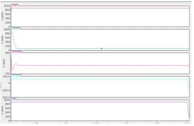
Fig. 4 Waveforms of Capacitive W-AC circuit
Here by DC analysis is done to get N-Curves shown in “Fig 4” when word line is high. Capacitive WA outline is used to scale supply to reduce cell stability.
2.1.2.1 Capacitive W-AC (Capacitive Write Assist Scheme)
In this pattern data can be written with high WM by altering the strength of the cell. Cell
This is the second write assist outline to make very easy write operation. Main aim of order is undershooting bit line to deliver negative source voltage to access transistor so as to run high channel width to write the data early means WM can be improved.
Fig .5 Transient-NBL write circuit
Fig. 6 For Cell supply voltage is 900mV
From “Fig 6” data can be driven into the cell is 1 when NBL driver circuitry make bit line is negative. In this transient negative bit line pattern write operation is achieved by increasing the power of SRAM pass transistor. When supply voltage of the cell is 900mV so that strength of the stored data is more than write data. So for 0 is written when Bit-en low and cell is not able to key. So cell strength has been compact to latch the state of the cell.
2.1.2.3 NBL scheme on the source of the write circuit
In this scheme write of data is accomplished by negative the bit line as before but change of this scheme is applied the negative bit-line power on source of the driver circuitry in its place of using coupling operation inside the driver circuitry.
Fig. 7 Source coupled NBL write circuit
Fig. 8 waveform of source coupled NBL write circuit
From above “Fig 8” data can be focused into cell is 1using NBL driver circuitry.
2.2 Read Assist Schemes
To improve both stability and performance of SRAM cell, it is main that the Bit line capacitive loading should be as low as possible. In this section we examine a new read-assist scheme for cell that will nullify the drawbacks of local sense amplifier. The proposed schemes improves the concert of sensing circuitry by amplifying the BL voltage drop and while sinking the BL voltage swing which results in significant power fall. Reduction in cell VDD with respect to the original scheme causes reduction in leakage power dissipation. These hitches can be overcome by following Read assists schemes.
2. 2.1 Proposed Read Assist scheme for 9-T SRAM Cell
Here while performing write operation to cell write driver circuitry is needed lengthwise with to perform read operation following read kit is needed
a. Sense amplifiers b. Isolation circuitry c. Pre-charge circuitry d. SRAM Cell
as to produce possible error to sense data using sense amplifier.
Fig. 9 Read assists Scheme with 6-T
2.2.2 9-T cell with all peripheral circuitry to write and read totally
Here RAPBG System is used to make read and write operation on cell with less power consumption. Proposed Technique is used by which cell solidity can be adjusted affording to the cell operation so that power degeneracy can be very low.
Here N,P Sense amplifiers are used to improve speed of operation by reducing sensing delay. So Speed and power intake requirement for any system can be attained using this read assist scheme.
Here Data which is stored in SRAM cell can be sensed using P,N Sense amplifiers after pre-charge operation is performed which is shown in “Fig 11”.
2.3 Standby Mode
Here write enable line should be zero. So two transistors in 9T SRAM cell are in off condition. Current is generally smooth between supplies to ground. We designed circuit to reduce leakage current and is designed in 45nm technology with sub-threshold voltage of 0.7V. Until and unless threshold voltage is 0.7V transistor is not switched ON.
3.Layouts
Fig. 10 Read assist Scheme with 9-T
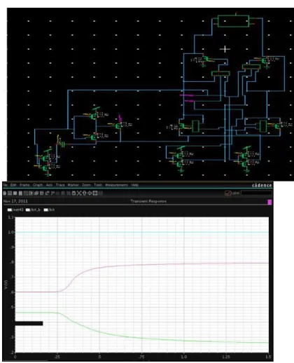
Fig.11 Waveforms Of Read Assist Sccheme
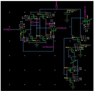
Fig. 12 Layout of 9T SRAM cell
4.
Results & Discussion
4.1 Power Calculations for 9-T SRAM Cell The delay and power controls are done
on this schematic 9-T SRAM cell
4.1.1 Calculation of delay
Write to bit b =52.33ps
Write to bit = 26.33ps
I. Calculation of power
Condition Power in watts
Initial 37.84×10⁻¹⁵
Write -“1”logic 123.5×10⁻¹⁵
Read-“1” logic 32.3×10⁻¹⁵
Write-“0” logic 118.4×10⁻¹⁵
Read-“0”logic 32.8×10⁻¹⁵
From above “Table 1” it is clear that power consumed by SRAM cell in write operation is more when likened to read operation.
4.2 Delay and leakage currents for 9-T SRAM cell are calculated. Cell is sized according to better
write and read margins.
4.2.1 Delay calculations Write in to bit-line=42.02ps. Write into bit-line-bar=35.4ps. 4.2.2 Calculation of currents I read=60.2 u A
I leakage=57.4 pA.
Here leakage power of the cell= I leakage x supply voltage (in standby mode)
=3.21 x 1 =3.21 uW.
II. Calculation of power
Conditions Power
(watts×10-
15)
Write Logic-1 102.2
Write Logic-0 92.3
Read Logic-1 52.3
Read Logic-0 42.9
From above “Table2” we can achieve that power consumed by SRAM cell for write operation is more than read operation. The write assist schemes to reduce the power consumption because we are planning low power SRAM so power consumption should less.
III. Calculation of power dissipation
Name of the
write Write margin(WM)
assist scheme Write trip voltage write trip current
Capacitive
W-AC 0.69V 5.8uA
Transient-NBL 0.62V 3.1uA
4.2.5 Write margin calculations
Write margin describes how fast the data is going to write and read margin is clear to know how fast the data is interpretation from the cell.
IV. Write margin
Supply Power dissipation(pW) voltage of the
cell
1 V 50.4
0.5 V 52.9
These values are calculated by using N-curves of the cell drawn by varying one node voltage from 0 to supply voltage and by doing DC analysis.
5. CONCLUSION
The operational transconductance amplifier (OTA) for implementing a LPF filter of cut off frequency. In this project a bulk driven Operational Trans conductance Amplifier with local common mode feedback is designed for ultra low power and low frequency applications. For further reduction of cut off frequency, capacitance multiplier is used. The filter designed consumes of power low power supply N well CMOS technology. Simulation results show significant improvement in power, linearity and total harmonic distortion. By using capacitance multiplier, the area used to implement the capacitor is reduced
References
[1] T. Maheswari, P. Sukumar. “Error Detection and Correction in SRAM Cell Using Decimal Matrix Code”, IOSR Journal of VLSI and Signal Processing (IOSR-JVSP), Jan 2015, pn 09-14.
[2] Rakhi R1, Abhijeet D. Taralkar2, Vasantha M.H.3, Nithin Kumar Y. B.4 A 0.5V low power OTC-C low pass filter For ECG detection
[3] MLAManikandan, M. Sabarimalai, and K. P. Soman. A novel method for detecting R-peaks in electrocardiogram (ECG) signal. Biomedical Signal Processing & Control., vol. 7, 2012, pp.118-128
.
.Copyrights © International Journal of Intellectual Advancements and Research in Engineering Computations, Analysis based Selective Coefficient Method.
Measurement. vol. 43, 2010, pp.255-261.
[5] P.Sukumar K.Sabeha, “Highly Secured System to Find the Improper Impression of Fingerprints in Hostel” International Journal for Scientific Research & Development.vol 3, no. 6, 2016. Advancements and Research in Engineering Computations, vol-5, pp 134-