Sudhir Dakey
Faculty ,Department of E.C.E., MVSR Engineering College
Abstract— The goal of VLSI has remained unchanged since many years and that is to reduce area to make the chips cheaper, reduce the delay to make them faster and to reduce power dissipation to make the more portable. There are many ways to reduce power dissipation in transistor level circuit but in recent years, new kind of gates called the reversible logic has emerged as a promising computing paradigm having application in low power CMOS, quantum computing, nanotechnology, and optical computing. The conventional gates are not reversible. To generate a useful gate function the Reversible Gates require constant inputs and some additional unused outputs, called Garbage Outputs, in order to maintain the reversibility of the digital circuits. In this paper, full adder using various reversible gates have been analysed using Xilinx 12.1 tool and implemented on Spartan 6 FPGA.
Keywords — Reversible gates, Peres Gate (PG), Feynman Gate (FMG), Fredkin Gate (FKG), HN Gate (HNG), TS Gate (TSG), Garbage Output (GO).
I. INTRODUCTION
The conventional gates are irreversible in nature, meaning the inputs cannot be constructed from the outputs. Such gates cause loss of information. Traditional combinational logic circuits dissipate heat for every bit of information lost during their operation. However, if the same circuit is constructed using the reversible logic gates (in gates where the inputs can be constructed from the outputs), the dissipation of heat can be reduced as per the demonstration of R. Landauer[1] in the 1960s. He showed that the loss per bit of information exchange is KTln2 Joules of energy where K is Boltzmann constant and T the absolute temperature at which the operation is performed. Later in 1973, Bennett[2] showed that this amount of energy loss can be overcome if the circuit is designed using the reversible logic. With the number of gates doubling every 18 to 24 months, as per Moore’s Law, the irreversible technologies would dissipate a lot of heat and reduce circuit life. For room temperature T,the amount of heat dissipated for one bit is small i.e. 2.9×10⁻²¹ J. For the current processors, assuming every transistor out of more than 4×10⁷ dissipates heat at the processor frequency of 2GHz, the figure becomes 2.3×10⁻⁴ J/sec which is quite a large quantity. A reversible logic gate is an n-input, n-output device with n-to-n mapping, which helps determining the outputs from the inputs and vice versa. Wherever necessary, extra outputs can be added to make the output count equal to that of the input. The major challenges lies in reducing the number of gates required, delay and the quantum cost of the reversible gate.
II. REVERSIBLE GATES
A. Peres Gate (PG)[3]
Figure 1: Peres Gate (PG)
B. Feynman Gate (FMG)[4]
Figure 2 shows a 2*2 Feynman Gate. The quantum cost of a Feynman Gate is 1. It is also known as Controlled Not (CNOT) Gate. It has quantum cost 1 and is generally used for Fan Out purposes.
Figure 2: Feynman Gate (FMG)
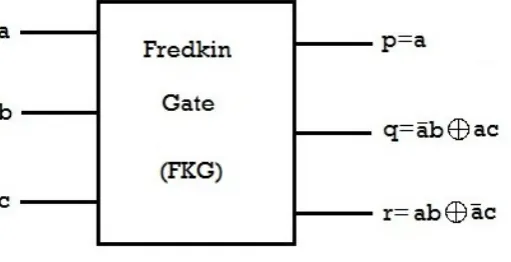
C. Fredkin Gate (FKG)[5]
Figure 3 shows a 3*3 Fredkin Gate. It has quantum cost 5. It can be used to implement a Multiplexer.
Figure 3: Fredkin Gate (FKG)
D. HN Gate (HNG)[6]
Figure 4: HN Gate (HNG)
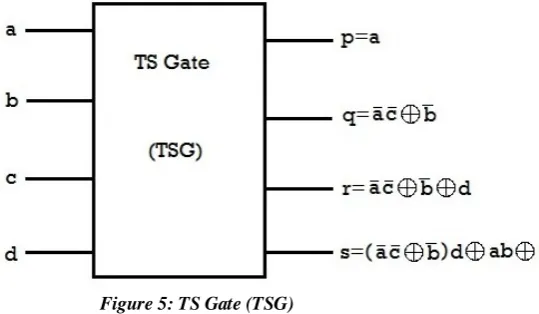
E. TS Gate (TSG)[7]
Figure 5 shows a 4*4 TS Gate. It is used for designing multipliers.
Figure 5: TS Gate (TSG)
III. FULL ADDER USING REVERSIBLE GATES
A. Full Adder using Peres Gate (PG)
The following convention will be followed in this paper. The inputs of first Peres Gate will be called as a1, b1, c1 and the outputs as p1, q1, r1. Similarly, the inputs of second Peres Gate as a2, b2, c2 and outputs as p2, q2, r2. In order to realize a full adder, we have to use 2 Peres Gates. The connections required are as follows. The inputs a, b, cin are connected to a1, b1 and b2. The outputs sum and cout are connected to q2 and r2. The input c1 is grounded, q1 is connected to a2 and r1 is connected to c2. There are two garbage outputs here which are p1 and p2.
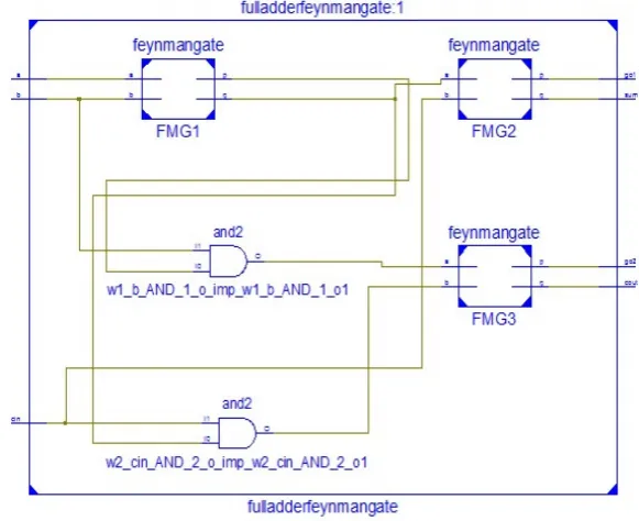
B. Full Adder using Feynman Gate (FMG)
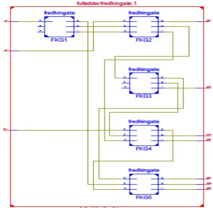
The Fredkin Gate is 3*3 gate which is not much suitable for a full adder. There are many ways to realize a full adder from it, there are 5 gates in the design I am using here. There are five garbage outputs which are p2, r3, r4, p5 and r5.
D. Full Adder using HN Gate (HNG)
This gate is one of most suitable reversible gates for a full adder. It takes only 1 HNG and there are two garbage outputs which are p1 and q1.
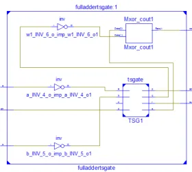
E. Full Adder using TS Gate (TSG)
This gate is most suitable reversible gate for multiplier design. It takes only 1 TSG and there is only one garbage output.
IV. SIMULATION RESULTS
A. Full Adder using Peres Gate (PG)
Figure 6: Simulation of Full Adder using Peres Gate (PG)
Figure 7: RTL schematic of Full Adder using Peres Gate (PG)
Figure 8: Simulation of Full Adder using Feynman Gate (FMG)
Figure 9: RTL schematic of Full Adder using Feynman Gate (FMG)
C. Full Adder using Fredkin Gate (FKG)
Figure 11: RTL schematic of Full Adder using Fredkin Gate (FKG)
D. Full Adder using HN Gate (HNG)
Figure 12: Simulation of Full Adder using HN Gate (HNG)
Figure 13: RTL schematic of Full Adder using HN Gate (HNG)
Figure 14: Simulation of Full Adder using TS Gate (TSG)
Figure 15: RTL schematic of Full Adder using TS Gate (TSG)
V. SYNTHESIS RESULTS
The designed full adder using various reversible gates are simulated and synthesized using Xilinx ISE 12.1 tool. This tool offers RTL schematic, Technology schematic, timing analysis and power analysis. Comparison of a full adder realized using various reversible gates is presented below in a table.
Table 1: Comparison of a full adder realized using various reversible gates
Reversible gate No. of gates No. of garbage outputs (GO) Delay(ns)
Peres Gate (PG) 6 2 0.781
Feynman Gate (FMG) 5 2 0.786
Fredkin Gate (FKG) 40 5 0.795
HN Gate (HNG) 6 2 0.781
TS Gate (TSG) 14 1 0.785
creating an reversible gate is endless. In recent times, many authors have proposed unique gates which serves a specific purpose.
As a further work, several other designs for reversible gates can be studied and can be utilized in designing the basic building blocks of a processor like multipliers, multiplexers etc. The reversible gates can be implemented in transistor level to optimize the performance.
REFERENCES
[1] Landauer, R., “Irreversibility and heat generation in the computing process”, IBM J. Research and Development, 5(3): pp. 183-191, 1961
[2] Bennett, C.H., “Logical reversibility of Computation”, IBM J.Research and Development, 17: pp. 525-532, 1973 [3] A. Peres, “Reversible logic and quantum computers”, Phys.Rev. A 32 (1985) 3266-3276
[4] R. Feynman, “Quantum Mechanical Computers”, Optic News, Vol 11, pp 11-20 1985
[5] E. Fredkin and T. Toffoli,"Conservative Logic", International Theoretical Physics Vo121, pp.219-253, 1982 [6] Shams, M., M. Haghparast and K. Navi, “Novel reversible multiplier circuit in nanotechnology” World Appl.
Sci. J.,3(5): 806-810