University of Pennsylvania
ScholarlyCommons
Publicly Accessible Penn Dissertations
1-1-2015
Manipulation of Light-Matter Interaction in
Two-Dimensional Systems via Localized Surface
Plasmons
Joohee ParkUniversity of Pennsylvania, [email protected]
Follow this and additional works at:http://repository.upenn.edu/edissertations Part of theMechanics of Materials Commons
This paper is posted at ScholarlyCommons.http://repository.upenn.edu/edissertations/1932
For more information, please [email protected].
Recommended Citation
Park, Joohee, "Manipulation of Light-Matter Interaction in Two-Dimensional Systems via Localized Surface Plasmons" (2015).
Publicly Accessible Penn Dissertations. 1932.
Manipulation of Light-Matter Interaction in Two-Dimensional Systems
via Localized Surface Plasmons
Abstract
Localized surface plasmons (LSPs), which are collective charge oscillation confined by metallic nanoparticles, gained much interest in the field of optoelectronics due to its ability to confine light down to nanoscale without a diffraction limit. As light-matter interaction in nanoscale is becoming more important due to the demand in scaling down the optoelectronic devices, my thesis describes the work on manipulation of such light-matter interaction enabled by LSPs. First, periodically patterned two-dimensional arrays of bowties were investigated to study the localized surface plasmon (LSP) resonances via reflection measurements and numerical simulations. Due to the grating created by arrays of bowties, a new, lattice-coupled LSP (lattice-LSP) mode emerged. Comparing the calculated E-field enhancement of the bowtie arrays to the reflection spectra showed that the lattice-LSP mode positions are closely related to the dips in the reflectance spectra. After the study of bowtie arrays, we showed photoluminescence (PL) from bulk, planar silicon coupled with metal bowtie nanocavities, which is an indirect bandgap semiconductor with very low emission efficiency. This was due to the E-field concentrated inside the tips of the metal bowtie achieved by LSPR, leading to increased radiative decay rate. The approach of bowtie-coupled emitter was also applied to monolayer MoS2, a transition metal dichalcogenide semiconductor which transforms to a direct bandgap semiconductor in monolayer. Silver bowtie array coupled with monolayer of MoS2 showed a high enhancement in emission (Raman and PL) due to surface-enhanced fluorescence (SEF) from weak-coupling of MoS2 excitons and bowtie's LSPR. By tailoring the design of bowtie arrays, we controlled the location of surface plasmon resonances which, coupled with MoS2 excitons, led to spectral modification of PL spectra. Furthermore, at low temperature, we achieved stronger coupling between the two systems in some designs of the bowtie array and observed Fano resonances in reflection measurements. The approach was extended to photocurrent studies in MoS2. Utilizing the helicity of monolayer MoS2 is suggested as future work to investigate the circular photocurrent in MoS2 induced by selective linear polarizations. Lastly, by fabricating nanoribbon arrays of fluorographene, evolution of localized surface plasmon mode of graphene in near-infrared
wavelength range was studied via Fourier transform infrared spectroscopy (FTIR). The initial result showed possibility of tunable graphene IR plasmon resonance depending on the array design due to the localized surface plasmon mode created by the grating of alternating fluoro-graphene and graphene nanoribbons, confining E-field to excite the plasmon modes in IR range.
Degree Type
Dissertation
Degree Name
Doctor of Philosophy (PhD)
Graduate Group
Materials Science & Engineering
First Advisor
Ritesh Agarwal
Keywords
2-D materials, light-matter interaction, localized surface plasmons, molybdenum disulfide, plasmonics
Subject Categories
Mechanics of Materials
MANIPULATION OF LIGHT-MATTER INTERACTION IN TWO-DIMENSIONAL SYSTEMS VIA LOCALIZED SURFACE PLASMONS
Joohee Park
A DISSERTATION
in
Materials Science and Engineering
Presented to the Faculties of the University of Pennsylvania
in
Partial Fulfillment of the Requirements for the
Degree of Doctor of Philosophy
2015
________________________
Supervisor of Dissertation
Ritesh Agarwal
Professor, Materials Science and Engineering (MSE)
_________________________
Graduate Group Chairperson
Shu Yang
Professor, Materials Science and Engineering (MSE)
Dissertation Committee
Charlie Johnson, Professor, Physics/MSE/ESE
Nader Engheta, H. Nedwill Ramsey Professor, ESE/MSE/Physics/BE
MANIPULATION OF LIGHT-MATTER INTERACTION IN TWO-DIMENSIONAL SYSTEMS VIA LOCALIZED SURFACE PLASMONS
COPYRIGHT
2015
Joohee Park
This work is licensed under the Creative Commons Attribution- NonCommercial-ShareAlike 3.0 License
To view a copy of this license, visit
iii
iv
ACKNOWLEDGMENT
First and foremost, I thank Professor Ritesh Agarwal, my advisor and mentor, for his
guidance throughout my doctorate years. It has been an honor to be his Ph.D student. I still
remember the first time I met him in his office, where he went through with enthusiasm the
interesting work going on in his group. He has taught me consciously and unconsciously how
good research should be done. His deep and keen insights have always guided me to the right
direction. I appreciate his contribution of time, ideas, and funding to make my Ph.D possible.
I want to thank all the members of Agarwal group for being the source of friendships,
good advice, and collaboration. Especially Dr. Bumsu Lee, my collaborator of 3 years who is the
most diligent person I know, has trained me by my side how good experiments should be done.
Without him, I would not have produced the results that we produced. I thank Dr. Chang-hee Cho
and Dr. Ho-seok Ee for aiding my studies. Dr. Ee, although his time in the group has been short,
has provided many calculation works which made our work possible. Rahul, who is my best
friend from the group and the department, has been there for me through all the tough times of
my Ph.D years. I will miss our chat-times on nice evenings at the rooftop of Singh center, with
our favorite beverages.
I want to thank my collaborators from Prof. Johnson's group. Dr. Gang-hee Han from
Johnson group provided the best quality samples so readily and made this work possible. I also
thank Carl Naylor for providing the carefully grown, best samples and being a very kind person
v
ABSTRACT
MANIPULATION OF LIGHT-MATTER INTERACTION IN TWO-DIMENSIONAL SYSTEMS VIA LOCALIZED SURFACE PLASMONS
Joohee Park
Ritesh Agarwal
Localized surface plasmons (LSPs), which are collective charge oscillation
confined by metallic nanoparticles, gained much interest in the field of optoelectronics
due to its ability to confine light down to nanoscale without a diffraction limit. As
light-matter interaction in nanoscale is becoming more important due to the demand in scaling
down the optoelectronic devices, my thesis describes the work on manipulation of such
light-matter interaction enabled by LSPs. First, periodically patterned two-dimensional
arrays of bowties were investigated to study the localized surface plasmon (LSP)
resonances via reflection measurements and numerical simulations. Due to the grating
created by arrays of bowties, a new, lattice-coupled LSP (lattice-LSP) mode emerged.
Comparing the calculated E-field enhancement of the bowtie arrays to the reflection
spectra showed that the lattice-LSP mode positions are closely related to the dips in the
reflectance spectra. After the study of bowtie arrays, we showed photoluminescence (PL)
from bulk, planar silicon coupled with metal bowtie nanocavities, which is an indirect
bandgap semiconductor with very low emission efficiency. This was due to the E-field
concentrated inside the tips of the metal bowtie achieved by LSPR, leading to increased
radiative decay rate. The approach of bowtie-coupled emitter was also applied to
monolayer MoS2, a transition metal dichalcogenide semiconductor which transforms to a
vi
of MoS2 showed a high enhancement in emission (Raman and PL) due to
surface-enhanced fluorescence (SEF) from weak-coupling of MoS2 excitons and bowtie's LSPR.
By tailoring the design of bowtie arrays, we controlled the location of surface plasmon
resonances which, coupled with MoS2 excitons, led to spectral modification of PL
spectra. Furthermore, at low temperature, we achieved stronger coupling between the two
systems in some designs of the bowtie array and observed Fano resonances in reflection
measurements. The approach was extended to photocurrent studies in MoS2. Utilizing the
helicity of monolayer MoS2 is suggested as future work to investigate the circular
photocurrent in MoS2 induced by selective linear polarizations. Lastly, by fabricating
nanoribbon arrays of fluorographene, evolution of localized surface plasmon mode of
graphene in near-infrared wavelength range was studied via Fourier transform infrared
spectroscopy (FTIR). The initial result showed possibility of tunable graphene IR
plasmon resonance depending on the array design due to the localized surface plasmon
mode created by the grating of alternating fluoro-graphene and graphene nanoribbons,
vii
TABLE OF CONTENTS
ABSTRACT ... V
TABLE OF CONTENTS ... VII
LIST OF ILLUSTRATIONS ... X
CHAPTER 1. INTRODUCTION ... 1
1.1 PLASMONS AND SURFACE PLASMONS ... 2
1.2 LIGHT-MATTER INTERACTION VIA LOCALIZED SURFACE PLASMONS ... 3
1.2.1 LOCALIZED SURFACE PLASMON RESONANCE (LSPR) FOR METALLIC NANOPARTICLES ... 4
1.2.2 EMITTER NEAR METAL NANOSTRUCTURES ... 6
REFERENCES ... 9
CHAPTER 2. STUDY AND OPTIMIZATION OF METAL BOWTIE AND BOWTIE ARRAY AS PLASMONIC NANOCAVITY ... 11
2.1 MOTIVATION: WHY STUDY A BOWTIE? ... 11
2.2 BACKGROUND: MORE THAN A SINGLE BOWTIE ... 13
2.3 METHODS ... 15
2.3.1 DEVICE FABRICATION ... 15
2.3.2 EXPERIMENTAL SETUP ... 15
2.3.3 NUMERICAL CALCULATION ... 15
2.4 RESULTS AND DISCUSSION ... 16
2.4.1 OPTIMIZATION OF BOWTIE FABRICATION ... 16
2.4.2 PLASMON RESONANCES IN BOWTIE ARRAY ... 18
2.5 CONCLUSION ... 28
REFERENCES ... 29
CHAPTER 3. PHOTOLUMINESCENCE FROM BULK, PLANAR SILICON COUPLED WITH SILVER BOWTIE NANOCAVITIES ... 31
3.1 MOTIVATION ... 31
viii
3.3 METHODS ... 37
3.3.1 DEVICE FABRICATION ... 37
3.3.2 EXPERIMENTAL SETUP ... 37
3.3.3 NUMERICAL CALCULATION ... 37
3.4 RESULTS AND DISCUSSION ... 38
3.5 CONCLUSION ... 41
REFERENCES ... 42
CHAPTER 4. FANO RESONANCE AND SPECTRALLY MODIFIED PHOTOLUMINESCENCE ENHANCEMENT IN MONOLAYER MOS2 COUPLED WITH BOWTIE PLASMONIC NANOANTENNA ARRAY ... 44
4.1 MATERIAL BACKGROUND ... 44
4.2 MOTIVATION ... 48
4.3 METHODS ... 50
4.3.1 DEVICE FABRICATION ... 50
4.3.2 EXPERIMENTAL SETUP ... 50
4.3.3 NUMERICAL CALCULATION ... 50
4.4 RESULTS AND DISCUSSION ... 51
4.5 CONCLUSION ... 69
REFERENCES ... 70
CHAPTER 5. PHOTOCURRENT IN MONOLAYER MOS2 ... 74
5.1 MOTIVATION ... 74
5.2 BACKGROUND ... 74
5.3 METHODS ... 79
5.3.1 DEVICE FABRICATION ... 79
5.3.2 EXPERIMENTAL SETUP ... 79
5.4 INITIAL RESULT AND FUTURE DIRECTION ... 80
5.5 CONCLUSION ... 84
REFERENCES ... 85
ix
6.1 BACKGROUND ... 86
6.2 MOTIVATION ... 92
6.3 METHODS ... 93
6.3.1 DEVICE FABRICATION ... 93
EXPERIMENTAL SETUP ... 93
6.4 INITIAL RESULT AND FUTURE DIRECTION ... 94
6.5 CONCLUSION ... 97
x
LIST OF ILLUSTRATIONS
Figure 1.1 | a, Surface plasmons on metal surface, which are transverse magnetic. b, The
exponentially decaying field perpendicular to the metal surface. δd and δm are the decay
length of the field into the dielectric and metal, respectively. c, Dispersion of a SP mode
showing momentum mismatch that must be overcome in order to couple light and SP modes. Reprinted with permission from ref. 2. © 2003, Nature Publishing Group.
Figure 1.2 | Plasmon oscillation of a sphere with the displacement of the conduction electron charge cloud with respect to the nuclei. Reprinted with permission from ref. 8. © 2003, American Chemical Society.
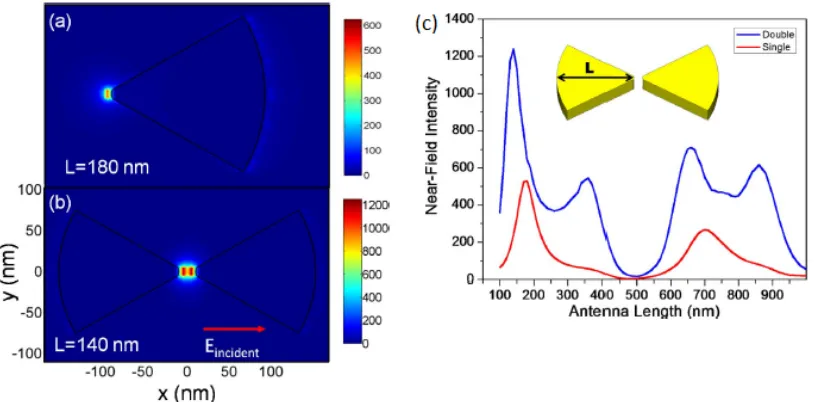
Figure 2.1 |a-b, Near-field intensity distribution in single triangular gold particle (a) and
coupled triangles (bowtie) (b). c, Near-field intensity of single and coupled triangles as a
function of triangle size, L. Reprinted with permission from ref. 3. © 2008, IEEE
Figure 2.2 | a-b, E-field distribution at the LSPR frequency for incident light polarized
along (a) and perpendicular (b) to the bowtie axis (g = 30 nm). c, Extinction spectra of
the bowtie nanoantenna for polarization parallel (solid curves) and perpendicular (dotted
curve) to the bowtie axis for different gaps. Reprinted with permission from ref. 8. ©
2014, Springer Science+Business Media New York
Figure 2.3 | a-b, Calculated extinction efficiencies from Au bowtie arrays under parallel polarization, with varying horizontal pitch distance (a) and the vertical pitch distance (b).
c, Electric field distribution at the LSPR frequency for the chosen bowtie array (both
pitch periods of 525 nm, gap of 30 nm). Reprinted with permission from ref. 8. © 2014, Springer Science+Business Media New York
Figure 2.4 | a, Schematic of metal-dielectric bowties on silicon substrate. b, Diagram of
nanosphere lithography. Reprinted with permission from ref. 9. © 1995, American
Vacuum Society c, SEM image of PS nanosphere dispersed on silicon substrate. d-e, SEM images of silver-SiO2 bowties made by nanosphere lithography.
Figure 2.5 | a-b, SEM images of bowtie structures after O2 plasma etching of the PS nanospheres and deposition of metal (30 nm Au) and interlayer oxide (5 nm SiO2).
Figure 2.6 | Schematic of bowtie array with gap separation, g, and side length, s. SEM example image of an underexposed (a), overexposed (b), and optimized (c) silver bowtie.
Figure 2.7 | a, Device schematic indicating the geometrical factors of a bowtie array: gap separation (g), side length of a triangle (s), and unit cell dimension or pitch (p = (px, py)).
b, Calculated extinction of a single bowtie (g = 20 nm, s = 100 nm) with the inset
displaying the E-field intensity profiles for TE and TM polarizations with respect to the
long axis of a bowtie. c, Calculated E-field enhancements in the array of bowties (s = 100
xi
TE or TM polarizations. Reprinted with permission from ref. 10. © 2015, American
Chemical Society.
Figure 2.8 | Polarization-dependent reflection spectra of the bowtie resonator array.
a, Normalized differential reflectivity (ΔR/R) spectra of experimental and calculated
lattice-LSP modes in TE and TM polarizations for bowtie array on SiO2/Si substrate.
Geometrical factors: s = 100 nm, g = 20 nm, p = (500 nm, 300 nm). b, Average E-field
enhancements for bowtie array on SiO2/Si calculated for the total area of the unit cell. Reprinted with permission from ref. 10. © 2015, American Chemical Society.
Figure 2.9 | Calculated average E-field enhancement, reflectance (ratio of reflected light
to incident light intensity), and ∆R/R spectra for the bowtie arrays on SiO2/Si substrate
with different pitch values (a-d). ∆R/R shows enhanced features due to subtraction of the
background. Bowtie geometrical factors: g = 10 nm, h = 50 nm, s = 100 nm. Reprinted with permission from ref. 10. © 2015, American Chemical Society.
Figure 2.10 | Pitch variation study of bowtie arrays. a, Incident light polarization (TE and TM) with respect to the bowtie axis direction. Table shows the pitch (px, py) values
for the 5 bowtie arrays (A-F). b, SEM images of the 5 bowtie arrays with pitch values
shown in (a). c-d, Experimental reflectance (∆R/R) for the 5 bowtie arrays measured in
TE and TM polarization. Bowtie geometrical factors: g = 20 nm, s = 100 nm.
Figure 2.11 | Calculated E-field enhancements of Ag bowtie arrays with varying pitch (p) values (solid curves), compared with the calculated extinction cross-section of a single bowtie (dotted curve) for TE polarization excitation. Bowtie geometry: gap separation (g) = 20 nm, thickness of the metal deposition (h) = 50 nm, side length of a triangle (s) = 100 nm. Reprinted with permission from ref. 10. © 2015, American Chemical Society.
Figure 2.12 | Bowtie gap variation study. a, Schematic of bowtie array patterns in
horizontal and vertical direction. b, SEM images of the 4 bowtie arrays with varying gap
separation (g = 20-80 nm). c-d, Reflection measurements for the 4 bowtie arrays
measured in TE (c) and TM (d) polarization. Bowtie geometrical factors: s = 100 nm, p = (500 nm, 300 nm).
Figure 3.1 | Hot luminescence from silicon coupled to a plasmon nanocavity. a, Schematic of the electronic band diagram of bulk crystalline silicon illustrating phonon-assisted hot luminescence processes before the thermalization of the carriers to the
minimum of the conduction band near the X-point. b, Schematic of an Ω-shaped
plasmonic nanocavity coupled silicon nanowire device. c, Scanning electron microscope
(SEM) image of the fabricated device. d and e, Optical images of a single-plasmonic
silicon nanowire device obtained through the glass substrate under white light (d), and a
focused laser excitation (e). f, Room-temperature photoluminescence spectra from single
silicon nanowire device coupled with Ω-shaped (magenta) cavity (100 nm Ag film)
having the silicon nanowire diameter, d, of 65 nm. Spectrum of a 5 nm SiO2 coated single
silicon nanowire without a plasmonic cavity (blue; d = 60 nm) is also shown, with no
xii ref. 20. © 2013,Macmillan Publishers Limited.
Figure 3.2 | Resonantly enhanced hot luminescence in plasmonic silicon. a,
Room-temperature photoluminescence spectrum from a single silicon nanowire coupled with Ω
-shaped plasmon nanocavity (d = 70 nm). The calculated frequency-dependent
electromagnetic field intensity inside the cavity reproduces the resonances correctly. b to
d, Calculated electric field profile at cavity resonance energies of 2.51 eV (b), 2.34 eV
(c), and (d) 2.18 eV labeled as A, B, and C on the spectrum, showing the formation of a
curved Fabry-Pérot like plasmonic cavity modes. The white outlines refer to the
Si-SiO2-Ag interfaces of the Ω-shaped cavity structure. Reprinted with permission from ref. 20. ©
2013,Macmillan Publishers Limited.
Figure 3.3 |a-b, SEM images of 30 nm gold bowtie structures fabricated by nanosphere
lithography and oxygen plasma etching. c, Room temperature PL spectra of gold bowtie
on bulk silicon compared with 30 nm thick gold film.
Figure 3.4 | Hot luminescence from planar silicon coupled with bowtie plasmon nanocavity. a, Room-temperature photoluminescence spectrum showing the visible hot luminescence collected from 4 bowtie plasmon nanocavities on planar silicon substrate. Calculated spectrum of energy-dependent field intensity is also shown. Inset; SEM image of the device showing planar single crystalline silicon coupled with Ag bowtie plasmon
nanocavities. Scale bar, 200 nm. b-c, Calculated electric field profiles in the bowtie
device. cross-sectional view (b) and top view (c) at a resonance energy of 2.32 eV. The
bowtie structure is outlined in white. Reprinted with permission from ref. 20. ©
2013,Macmillan Publishers Limited.
Figure 4.1 | a, Atomic structure of TMDS. b, Calculated electronic band structures of
bulk, bilayer, and monolayer MoS2. Reprinted with permission from ref. 46. © 2011,
American Physical Society.
Figure 4.2 |a-b, Optical (a) and photoluminescence (b) images of suspended monolayer
and few layer MoS2 on Si with etched holes. c, PL spectra of monolayer and bilayer
MoS2. d, Normalized PL of 1-6 layer MoS2. Reprinted with permission from ref. 1. ©
2010, The American Physical Society
Figure 4.3 | a, Raman spectra of thin and bulk MoS2 films. b, Two Raman active modes (E12g and A1g) in the unit cell of MoS2 shown along [1000] direction. Reprinted with permission from ref. 3. © 2010, American Chemical Society.
Figure 4.4 | MoS2 on SiO2/Si substrate prepared by mechanical exfoliation. a-c,
xiii
Figure 4.5 | a, Normalized PL emission from monolayer MoS2 under excitation by 458
nm and 532 nm laser. b, PL emission spectra from monolayer, bilayer, and bulk MoS2.
Figure 4.6 | Optical properties of monolayer MoS2-bowtie resonator array system at
room-temperature. a, Scanning electron microscope (SEM) image showing the silver bowtie array directly patterned on well-defined, stacked triangular flakes of mono- and bi-layer MoS2. Larger triangular flake of darker contrast corresponds to a single layer and
smaller flake of lighter contrast to a bilayer. b, Device schematic indicating the
geometrical factors of a bowtie array: gap separation (g), thickness of the metal deposition (h), side length of a triangle (s), and unit cell dimension or pitch (p = (px, py)).
c, Raman scattering spectra of bare MoS2, bowtie array, and bowtie-MoS2. Geometrical
factors: g = 20 nm; h = 50 nm; s = 100 nm; p = (500 nm, 300 nm). For all bowtie arrays
studied throughout the paper, g = 20 nm and h = 50 nm. d, PL spectra of bare MoS2,
bowtie array, and bowtie-MoS2.Inset shows PL in log scale. Reprinted with permission
from ref. 10. © 2011, American Physical Society.
Figure 4.7 | Polarization-dependent reflection spectra of the bowtie resonator array and emission spectra of MoS2 coupled with bowtie resonator array. a, Normalized
differential reflectivity (ΔR/R) spectra of experimental and calculated lattice-LSP modes
in TE and TM polarizations for bowtie array on SiO2/Si substrate. Geometrical factors: s
= 100 nm, p = (500 nm, 300 nm). b, Average E-field enhancements for bowtie array on
SiO2/Si calculated for the total area of the unit cell c, Experimental emission (PL and
Raman) spectra for bowtie-MoS2 system. Inset; zoomed-in spectra near the Raman active
region. d, Optical microscope image of bowtie arrays patterned in two orthogonal
orientations on a MoS2 flake. e, 2-D intensity scans measured at the Raman mode and
A-exciton energies. Scanning area indicated in d. Data in e shows different polarization
response for Raman (horizontally patterned bowties) and A-exciton emission (vertically
patterned bowties). Reprinted with permission from ref. 10. © 2011, American Physical
Society.
Figure 4.8 | Spectral modification of MoS2 photoluminescence coupled with bowtie
resonator arrays with different lattice-LSP dipole resonances at room temperature.
a,SEM images of four bowtie-array samples with different bowtie sizes and pitch values:
(i) s = 100 nm, p = (400 nm, 500 nm) (ii) s = 100 nm, p = (400 nm, 300 nm) (iii) s = 100
nm, p = (300 nm, 200 nm) (iv) s = 170 nm, p = (500 nm, 800 nm). b, ΔR/R spectra
associated with the lattice-LSP modes of the four different bowtie patterns on SiO2/Si
substrates. c, PL spectra of bare MoS2 (black) and four different patterns. d,
Wavelength-dependent PL enhancements (ratios of PL obtained for bowtie-MoS2 sample to PL of bare MoS2) for the four patterns on monolayer MoS2. Inset shows the enhancement of
A-exciton emission for all four patterns. e,Normalized PL spectra of bare MoS2 (black) and
the four different bowtie patterns on MoS2. Reprinted with permission from ref. 10. ©
2011, American Physical Society.
xiv
= (300 nm, 200 nm). Reprinted with permission from ref. 10. © 2011, American Physical Society.
Figure 4.10 | Lattice-LSP mode dependent spectrally modified PL enhancements of
MoS2 coupled to Ag bowtie arrays. Top panel shows the ∆R/R spectra of bowtie arrays
with different geometrical factors and polarization, as noted above each spectrum. Bottom panel shows PL spectra of bowtie-MoS2 samples from the corresponding bowtie array. Reprinted with permission from ref. 10. © 2011, American Physical Society.
Figure 4.11 | Fano resonance in the reflection spectrum of bowtie-MoS2 at 77 K.
Bowtie geometry: TE mode, s = 100 nm, p = (300 nm, 200 nm). a and b. Experimental
and calculated ∆R/R spectra for bare MoS2, bowtie array, and bowtie-MoS2 system. Clear
Fano resonances are observed at the A- and B-exciton spectral region. Inset in b shows
the schematic for the mechanism of observed Fano resonance in the exciton-plasmon
system. c, Calculated absorption spectra for the bare MoS2 (black), bowtie array (blue),
MoS2 in the combined bowtie-MoS2 system (green), and the bowtie in the combined bowtie-MoS2 system (red). The dotted circle highlights the region of MoS2 excitons
where Fano resonances are observed in the refection spectra in a. Reprinted with
permission from ref. 10. © 2011, American Physical Society.
Figure 4.12 | Controlling Fano spectra of the bowtie-MoS2 system by tuning the
lattice-LSP modes to overlap with MoS2 excitons at 77 K. a-c, Experimental ∆R/R
spectra of bare MoS2, bowtie, and bowtie-MoS2 system for three different samples with the following excitation polarization and geometrical factors. TE polarization, s = 100
nm, p = (400 nm, 300 nm) (a), TM, s = 140 nm, p = (500 nm, 400 nm) (b), TE, s = 100
nm, p = (800 nm, 700 nm) (c). Clear Fano resonances are observed when the bowtie
lattice-LSP modes overlap with MoS2 excitons. Reprinted with permission from ref. 10.
© 2011, American Physical Society.
Figure 5.1 | Valley-spin coupling in monolayer MoS2. In monolayer, the lowest-energy conduction bands and the highest-energy valence bands labelled by the z-component of their total angular momentum. The spin degeneracy at the valence-band edges is lifted by
the spin–orbit interactions. The valley and spin degrees of freedom are coupled. In
bilayer, spin degeneracy of the valence bands is restored by spatial inversion and time-reversal symmetries. Valley and spin are decoupled.. Reprinted with permission from ref. 5. © 2012, Macmillan Publishers Limited.
Figure 5.2 | a-c, Monolayer MoS2 is excited by a laser with excitation energy 1.96 eV
with left circularly polarized light. d-f, Bilayer MoS2 with same condition as (a).
Reprinted with permission from ref. 5. © 2012, Macmillan Publishers Limited.
Figure 5.3 | a, Top: SEM image of MoS2 device coated with silica-gold nanoshells (AuNS) with inset displaying manified image of the AuNS. Scale bar: 5 um. Bottom:
schematic of the MoS2 phototransistor with inset showing nanoshells on MoS2. b,
Photocurrent spectra of MoS2 monolayer before (red) and after (green) dispersing AuNS.
xv
d, SEM of Au electrodes and AuNS on MoS2 showing the laser scan area for the
photocurrent maps to the right. Scale bar: 5um. A source-drain voltage of 1 V and a gate voltage of 80 V is applied as shown by the circuit illustration. Three different laser wavelengths 645 nm, 680 nm, and 750 nm are used to raster the device and map the photocurrent. Reprinted with permission from ref. 6. © 2014, AIP Publising LLC.
Figure 5.5 | a-b, Bright (a) and dark field (b) optical images of the electrodes patterned on monolayer of MoS2. The dark field image shows patterning inside the left pair of
electrodes which is bowtie array. c, Initial photocurrent measurement (I-V curves) of
bowtie-MoS2 compared to that of bare MoS2 excited by He-Ne laser.
Figure 5.6 | a, Diagram of a metal bar showing excitation (red) and two plasmonic
modes (blue). b, Resulting circular polarization (black arrow) of light when the bar is
excited by incident light with the wavelength of Mode A, polarized in the direction
shown. c, Resulting circular polarization (black arrow) of light that is opposite of (b)
when the bar is excited by incident light with the wavelength of Mode A, polarized in the perpendicular direction with respect to the direction in (b).
Figure 6.1 | a, SEM image of graphene flake showing zigzag and armchair edges. . Reprinted with permission from ref. 1. © 2007, Nature Publishing Group. b, Graphene
electronic dispersion. Reprinted with permission from ref. 2. © 2009, The American
Physical Society.
Figure 6.2 | Raman of graphene. Reprinted with permission from ref. 4. © 2006, The American Physical Society.
Figure 6.3 | Transmission spectra of a, a glass/Al2O3, b, glass/graphene/Al2O3, c,
glass/Al2O3/particles, d, glass/graphene/Al2O3/particles, with various thicknesses of
Al2O3. The insets illustrate the cross section view of the device structure. The arrow in
(d) shows a shift in the resonance wavelength. Reprinted with permission from ref. 6. ©
2012, American Institute of Physics.
Figure 6.4 | Control of plasmon resonance through electrical gating and microribbon width. (a) IR transmission spectra of ribbons with 4um width, as gate voltage is varied from -0.3 to -2.2eV. (b) Terahertz plasmon resonance through electrical gating. Radiation polarized perpendicular to the graphene ribbons. (c) AFM images of graphene microribbon. (d) Transmission spectra of different ribbon widths for the same doping
concentration. Reprinted with permission from ref. 7. © 2011, Macmillan Publishers
Limited.
Figure 6.5 | Infrared nano-imaging of tapered graphene nanoribbon. a, Diagram of IR nano-imaging experiment of graphene on SiO2. Green and blue arrow indicate the incident and back-scattered light, respectively. Concentric circles on the surface of the
graphene show plasmon waves launched by the AFM tip. b–e, Images of IR amplitude s
xvi
bilayer graphene (white dashed line), which all act as scattering sites. Scale bars, 100 nm. Reprinted with permission from ref. 9. © 2012, Macmillan Publishers.
Figure 6.6 | Gate-induced modulation of transmission in graphene nanoribbon arrays
normalized to transmission spectra at the charge neutral point (CNP). a,
Nanoribbon-width dependence of optical transmission with EF = −0.37 eV. Nanoribbon width is
varied from 15 to 80 nm. b, Fermi level dependence of optical transmission in 50
nm-wide graphene nanoribbon array. EF is varied from −0.22 to −0.52 eV. The dotted vertical
lines indicates the zone-center energy of the in-plane optical phonons of graphene. Reprinted with permission from ref. 13. © 2013, American Chemical Society.
Figure 6.7 | a, Optical image of fluorographene square patterns on transferred graphene. Inset shows a magnified image of patterned fluorographene-graphene nanoribbon arrays.
b, Raman spectra of CVD graphene showing the characteristic D, G, and 2D peaks, as
expected, and of fluorographene which lost its graphene characteristics.
Figure 6.8 | a, Transmission spectra for 600 nm-width arrays of graphene and fluorographene, doped with F-SAM. The spectra were measured three consecutive times.
b,Transmission spectra for 400 nm-width arrays of graphene and fluorographene, doped
1
Chapter 1. Introduction
Localized surface plasmons (LSP), coherent oscillations of electrons confined at
the metallic interface of small nanoparticles, gained much interest in the field of
optoelectronics due to its ability to concentrate light down to nanoscale without a
diffraction limit. Since the recent advances in fabrication of nanoscale structures,
LSP-enabled matter interaction has been widely studied. Thus, manipulation of
light-matter interactions in nanoscale systems is critical for obtaining new optoelectronic
functionalities and flexible devices. In this thesis, my work on two-dimensional
manipulation of light-matter interaction in three materials systems, silicon, and MoS2,
and graphene, will be presented. In this chapter, concepts for the major constituents of
my thesis will be discussed in order to set the base of understanding for the chapters to
follow. Background on plasmons and how the plasmons confined by metal
nanostructures, localized surface plasmon (LSP), enable interesting light-matter
interaction when coupled to an emitter will be presented, as well as some of the important
previous work. In the following chapters, study of plasmonic bowtie array structures will
be presented, followed by the investigation of LSP-enabled manipulation of light-matter
interaction in silicon and monolayer MoS2 through the bowtie structures. Next, study of
photocurrent in MoS2 as well as study of IR plasmons in graphene-fluorographene
nanoribbon arrays will be presented with future directions. Material-specific backgrounds
will be included at the beginning of each corresponding chapter to help readers gain
understanding of plasmonic properties in each material relating to the results and
2
1.1 Plasmons and surface plasmons
The optical properties of materials are dictated by the complex dielectric function
of the material, 𝜀(𝑤,𝑘), a function of frequency and wavevector. Assuming the
wavelength of light incident on a material is much larger than the atomic unit cell
spacing, the dielectric function may be considered only of a function of energy, which
generally still holds true for metals up to UV frequencies1. By assuming the time-varying
E-field driving the free electron gas of a metal, the free-electron model, or Drude model,
describes the dielectric function of metals as following22,23: 𝜀 𝑤 = 𝜀!− !!!
!!! !"#.
Here 𝜀! = static permittivity, 𝑤! = electron plasma frequency, 𝛾 = damping coefficient.
Generally, the highly mobile electrons in the bulk metal can undergo collective
oscillations which behave as plasmons23.
When plasmons are driven at the interface of the metal and a dielectric such as air
and glass (Fig. 1.1a), they have a dispersion such as shown in Fig. 1.1c, calculated from
solving the Maxwell’s equation at the boundary between metal and dielectric surface for
the propagating wave confined at the interface1,2. This is known as surface plasmons
(SPs)1. This oscillation is resonantly driven at specific optical frequencies to produce a
strong charge displacement and associated field concentration. The field component
perpendicular to the surface is evanescent, decaying exponentially with distance away
from the surface, thus helping power to be contained within the vicinity of the metal (Fig.
3
Figure 1.1 | a, Surface plasmons on metal surface, which are transverse magnetic. b, The
exponentially decaying field perpendicular to the metal surface. δd and δm are the decay
length of the field into the dielectric and metal, respectively. c, Dispersion of a SP mode
showing momentum mismatch that must be overcome in order to couple light and SP modes. Reprinted with permission from ref. 2. © 2003, Nature Publishing Group.
1.2 Light-matter interaction via localized surface plasmons
Conventionally, dielectric lenses and resonators have been widely used to
manipulate and confine light in a very small volume for numerous applications including
low threshold lasers, sensors, and nonlinear optics. There has always been a demand in
scaling down the optical resonators even further in order to confine light more and
enhance light-matter interaction to achieve photonic devices for compact integrated
optical circuits. However, due to the fundamental laws of diffraction, the focus of light in
these dielectric optical resonators are limited only down to (λ/2)3, where λ is the
wavelength of light inside the dielectric medium3. Thus, optical resonators that can
sustain surface plasmons and localize the electromagnetic (EM) energy in subwavelength
scale are critical in achieving extreme concentration and manipulation of light for
applications in optical biosensing, light harvesting, and optical nanoantennas. In most
4
photonic crystals, in which light is confined due to refractive index mismatch between the
material and the surrounding4-6. When a metallic cavity interacts with light, the surface
plasmons localize at the metal surface, called localized surface plasmons (LSPs). The
energy of LSP resonance (LSPR) depends on the design (size, geometry, and material) of
the nanostructures as well as on the surrounding dielectric environment7.
1.2.1 Localized surface plasmon resonance (LSPR) for metallic nanoparticles
When light is irradiated on a metallic nanoparticle, the oscillating electric field
induces SPs. This collective oscillations are known as localized surface plasmon
resonances (LSPRs)21. The electron cloud is displaced relative to the nuclei leading to a
restoring force due to Coulomb attraction between electrons and nuclei (Fig. 1.3). This
leads to drastic change in the incident radiation pattern and interesting effects such as
formation of high intensity hot spots on the nanoparticle surface and directional scattering
of light12.
5
The density of electrons, effective electron mass, and the shape and size of the
charge distribution determine the oscillation frequency8. This collective oscillation of the
electrons in the spherical metallic nanoparticle is called the dipole plasmon resonance of
the particle. To relate the dipole plasmon frequency of a metal nanoparticle to the
dielectric constant, interaction of light with a spherical particle of radius a that is much
smaller than the wavelength of light is considered. In this scheme, the electric field of the
light can be assumed as constant, called quasistatic approximation. Using the
wavelength-dependent dielectric constant of the metal particle, εi, and of the surrounding
medium, εo, the polarizability, α, is given by the following8.
α = gda3; gd = !!! ! !!
! ! !!! (1)
As a radiating dipole, the particle contributes to extinction and Rayleigh scattering by the
sphere (Mie theory states extinction = scattering + absorption)8-10. The extinction and
scattering efficiencies, Qext and Qsca, are given by the following with x = 2πa(εo)1/2/λ.
Qext = 4xIm(gd) (2)
Qsca = !!𝑥! 𝑔
! ! (3)
The efficiency is the ratio of the cross-section to the geometrical cross-section (πa2). The
scattering and absorption cross-sections, Csca and Cabs, are given by the following.
𝐶!"# = !!!𝑘!𝑎! 𝑔
! ! (4)
𝐶!"#= 4𝜋𝑘𝑎! 𝐼𝑚𝑔
6
It can be seen from the expression of gd that the resonant enhancement occurs when
𝜀!+2𝜀! is minimum, that is, 𝑅𝑒 𝜀! 𝑤 =−2𝜀! (Frohlich condition). At this
condition, both scattering and absorption are highly enhanced. Moreover, for small
particles (a << λ), absorption dominates over scattering whereas scattering dominates for
larger particles. In the latter case, which most relates to fabricated metallic
nanostructures, strongly enhanced E-field forms due to scattering resonance.
1.2.2 Emitter near metal nanostructures
We have seen in the previous chapter that strong E-field can be concentrated by
metal nanoparticles at resonant conditions. Such LSPRs can also couple to the E-field
emitted by materials in the vicinity of the metal nanostructures, leading to increase in the
localized density of states (LDOS) and thereby strong modification of the radiative and
nonradiative decay properties of the emitter16,17. The two systems will interact with each
other and the optical properties of the emitter can be manipulated11.
Let us consider an emitter placed in a cavity. Depending on the parameters of the
cavity such as dimensions, shape, and composition, certain electromagnetic modes will
be supported. Thus, the cavity will allow only those final states as photons' decay
channels. For example, the DOS will be maximum at the LSPR wavelength for an emitter
placed close to a metal nanoparticle12. An important concept to understand regarding how
decay rate of an emitter is modified by the presence of a cavity is Purcell effect13,17,
which describes an enhancement of spontaneous emission rate of atoms resonant in a
7
effectiveness of light-matter interaction by quantifying the dissipation of energy inside
the cavity. The Purcell factor is given by the following:
𝐹! = !!!"#
!"## = ! !!!𝑄
!!
!!! (6)
where !! is the wavelength of light inside the cavity with refractive index, n, Q is the
quality factor, and V is the mode volume of the cavity. It is the ratio of the decay rate of
the emitter in the cavity, γcav, to that in free space, γfree. Thus, when FP > 1 the emission,
or spontaneous decay rate, is increased whereas otherwise the cavity limits the emission.
Quality factor describes the spectral mode energy density and is given by w/∆w, where w
is the center frequency (resonant) and ∆w is the full-width half-maximum (FWHM) of
the Lorentzian peak profile. Physically, it describes the energy loss relative to the stored
energy in the cavity per oscillation cycle, or how damped the system is. Mode volume, V,
describes the spatial confinement of light in the cavity. It is calculated by the ratio of the
total energy of the SP mode divided by the energy density at the position of highest
field1,15. Plasmonic structures, or cavities, without high quality factors can still induce a
strong enhancement of the decay rate in the emitters given their mode volume is highly
reduced. This is achieved as the plasmonic structures confine E-field into subwavelength
volumes, modifying the mode volume as given by !!!!! .
Similarly, the fluorescence of the emitter is modified by its optical
environment18,19, which leads to changes in the frequency-dependent spontaneous
8
enhanced, also called Surface Enhanced Fluorescence (SEF)19,20. In SEF, the emitter’s
absorption enhances due to in-coupling and excitation rate increase. The emitter’s
radiative decay rate is also enhanced due to strong local field from the metal
nanostructures. For example, for a dye molecule, the fluorescence enhancement, FSEF, of
the detected signal is given by the following.
(6)
Here, Eo is incident E-field, Eloc is local E-field at the molecule position, η and ηo is the
quantum efficiency of the molecule14 near and far from the nanostructure, respectively,
and u is the transition dipole moment. The quantum efficiency is defined as follows.
(7)
It is the ratio between the radiative decay rate, Γr, and the total decay rate of the
molecule, Γ, which is the sum of the radiative and nonradiative decay rates, Γnr. The
nonradiative decay rate reflects the absorption and intrinsic losses of the metal
nanostructures. In a hot spot where Eloc is much larger than Eo, eq. 6 suggests strongly
enhanced fluorescence. However, the highest fluorescence enhancement is obtained when
both (η/ηo) and Eloc are amplified.
9
References
1. Maier, S. 2007. Plasmonics. New York: Springer.
2. Barnes, W., Dereux, A. & Ebbesen, T. Surface plasmon subwavelength optics.
Nature 424, 824-830 (2003).
3. Schuller, J., Barnard, E., Cai, W., Jun, Y., White, J. & Brongersma, M. Plasmonics
for extreme light concentration and manipulation. Nat Mater 9, 368-368 (2010).
4. Cho, C., Aspetti, C., Park, J. and Agarwal, R. 2013. Silicon coupled with plasmon
nanocavities generates bright visible hot luminescence. Nature photonics, 7 (4), pp.
285-289.
5. Oulton, R., Sorger, V., Zentgraf, T., Ma, R., Gladden, C., Dai, L., Bartal, G. &
Zhang, X. Plasmon lasers at deep subwavelength scale. Nature 461, 629-632 (2009).
6. Min, B., Ostby, E., Sorger, V., Ulin-Avila, E., Yang, L., Zhang, X. & Vahala, K.
High-Q surface-plasmon-polariton whispering-gallery microcavity. Nature 457,
455-458 (2009).
7. Calderón, J., Álvarez, J., Martinez-Pastor, J. & Hill, D. Polarimetric Plasmonic
Sensing with Bowtie Nanoantenna Arrays. Plasmonics 10, 703-711 (2014).
8. Kelly, K., Coronado, E., Zhao, L. & Schatz, G. The Optical Properties of Metal
Nanoparticles: The Influence of Size, Shape, and Dielectric Environment. J. Phys.
Chem. B 107, 668-677 (2003).
9. Mie, G. Ann. Phys. 1908, 25, 377.
10. Bohren, C. F.; Huffman, D. R. Absorption and Scattering of Light by Small
Particles; Wiley Interscience: New York, 1983.
11. Kinkhabwala, A. et al. Large single-molecule fluorescence enhancements produced
by a bowtie nanoantenna. Nature Photon. 3, 654-657 (2009).
12. Giannini, V., Fernandez-Dominguez, A.I., Heck, S.C. & Maier, S.A. Plasmonic
nanoantennas: fundamentals and their use in controlling the radiative properties of
nanoemitters. Chem. Rev. 111, 3888-3912 (2011).
13. Purcell, E.M. Spontaneous emission probabilities at radio frequencies. Phys. Rev.
69, 681 (1946).
14. Kühn, S., Håkanson, U., Rogobete, L. & Sandoghdar, V. Enhancement of
10
15. Colas Des Francs, G., Derom, S., Vincent, R., Bouhelier, A. and Dereux, A. 2012.
Mie plasmons: modes volumes, quality factors, and coupling strengths (Purcell factor) to a dipolar emitter. International Journal of Optics, 2012.
16. Chen, Y., Munechika, K. & Ginger, D. Dependence of Fluorescence Intensity on the
Spectral Overlap between Fluorophores and Plasmon Resonant Single Silver
Nanoparticles. Nano Letters 7, 690-696 (2007).
17. Blanco, L. & García de Abajo, F. Spontaneous light emission in complex
nanostructures. Physical Review B 69, (2004).
18. Fort, E. & Grésillon, S. Surface enhanced fluorescence. Journal of Physics D:
Applied Physics 41, 013001 (2007).
19. LeRu, E., Etchegoin, P., Grand, J., Felidj, N., Aubard, J. & Levi, G. Mechanisms of
Spectral Profile Modification in Surface-Enhanced Fluorescence. J. Phys. Chem. C
111, 16076-16079 (2007).
20. Ming, T., Chen, H., Jiang, R., Li, Q. & Wang, J. Plasmon-Controlled Fluorescence:
Beyond the Intensity Enhancement. J. Phys. Chem. Lett. 3, 191-202 (2012).
21. Muhlschlegel, P. Resonant Optical Antennas. Science 308, 1607-1609 (2005).
22. Frank L. Pedrotti, L. S. P., Leno M. Pedrotti. Introduction to Optics. 3rd edn,
(Pearson Addison Wesley, 2007).
23. Kittel, C. & McEuen, P. Introduction to solid state physics. 8th edn, (J. Wiley,
11
Chapter 2. Study and optimization of metal bowtie and bowtie array as
plasmonic nanocavity
This chapter is reprinted in parts with permission from “Lee, B.*, Park, J.*, Han,
G., Ee, H., Naylor, C., Liu, W., Johnson, A. & Agarwal, R. Fano Resonance and
Spectrally Modified Photoluminescence Enhancement in Monolayer MoS2 Integrated
with Plasmonic Nanoantenna Array. Nano Letters 15, 3646-3653 (2015)”. Copyright
(2015) American Chemical Society.
2.1 Motivation: Why study a bowtie?
We have seen in the previous chapter that metallic nanocavity which can sustain
localized surface plasmon resonance (LSPR) can focus light into extremely small volume
without diffraction limit. Along with the ease of integration into devices, 2-D thin-metal
nanocavity was chosen to study the plasmonic effect in emitters. Among the nanocavity
designs, a bowtie structure consisting of two coupled thin-film metal triangles was
chosen as plasmonic metallic nanocavity for the study of light-matter interaction in the
materials to be discussed later. In a bowtie nano-resonator, the paired metal triangles
build up charges at the apexes (Fig. 2.1b), analogous to a capacitor due to the lightening
rod effect, leading to very strong near-field confinement compared to a single triangle
(Fig. 2.1c). It has also been shown to sustain strong LSP modes in comparison to other
geometries such as single rod or coupled rods1-3,13. Therefore, it will be beneficial if we
can incorporate the bowtie structures, with right geometry and design, into a material
system in order to activate the LSPRs and thus study how the light behaves in such
12
Figure 2.1 |a-b, Near-field intensity distribution in single triangular gold particle (a) and
coupled triangles (bowtie) (b). c, Near-field intensity of single and coupled triangles as a
function of triangle size, L. Reprinted with permission from ref. 3. © 2008, IEEE
Recently, experimental studies and calculation of single metal bowtie have been
reported, suggesting that greatly enhanced absorption and an increased radiative emission
rate lead to enhancement of the intrinsic quantum efficiency of the bowtie2,8,12,13. Figure
2.2 shows the numerical simulations of a single gold bowtie nanoantenna. Extinction
efficiency spectra calculated for different bowtie gap separations show that, in
polarization along the bowtie axis, the LSPR of a bowtie redshifts as the gap separation
decreases. This is contrary to the case where polarization is perpendicular to the bowtie
axis (higher energy plasmon resonance), where the redshift is absent. These lower and
higher energy plasmon resonances are characteristics of a bowtie as a single-particle and
13
Figure 2.2 | a-b, E-field distribution at the LSPR frequency for incident light polarized
along (a) and perpendicular (b) to the bowtie axis (g = 30 nm). c, Extinction spectra of
the bowtie nanoantenna for polarization parallel (solid curves) and perpendicular (dotted
curve) to the bowtie axis for different gaps. Reprinted with permission from ref. 8. ©
2014, Springer Science+Business Media New York
2.2 Background: More than a single bowtie
When the bowties are periodically patterned into a 2-D array, the plasmonic
near-fields of individual bowties interact with neighboring bowties leading to collective LSP
resonances from this 2-D plasmonic crystal. Coherent coupling between the bowtie’s
14
narrower than that of a singlebowtie4-7. This is explained by Wood anomaly arising from
the diffraction condition of the pattern4.
Figure 2.3 | a-b, Calculated extinction efficiencies from Au bowtie arrays under parallel polarization, with varying horizontal pitch distance (a) and the vertical pitch distance (b).
c, Electric field distribution at the LSPR frequency for the chosen bowtie array (both
pitch periods of 525 nm, gap of 30 nm). Reprinted with permission from ref. 8. © 2014, Springer Science+Business Media New York
Although numerical simulation of LSPR in metal bowtie array excited in a single
polarization has been reported8, more systematic studies can be performed including
experimental investigation. In this chapter, thorough understanding of LSPR in bowtie
arrays will be demonstrated through experiments and the results will be corroborated by
numerical calculations. By changing the design on bowtie arrays as well as polarization
of light exciting the bowties, the spectral positions and linewidths of lattice-LSP modes
will be modified over a broad optical range. This will enable selective, controllable
modification of emission characteristics of an optical emitter and serve as a powerful
method to tailor the light-matter interaction in the coupled system of bowtie array and the
15
2.3 Methods
2.3.1 Device fabrication
For nanosphere lithography, polystyrene (PS) beads with 350 nm diameter were
dispersed on silicon substrate. 5 nm SiO2 interlayer was deposited by atomic layer
deposition (ALD) followed by deposition of 30 nm-thick silver by e-beam evaporator
(Lesker PVD 75). The PS beads were lifted off by dissolving in CH2Cl2 with sonication
for 1 min. For etching of PS beads, oxygen plasma was used.
For electron-beam lithography, a single layer of PMMA A2 950 e-beam resist
was spincoated and the bowties were patterned on silicon or SiO2/Si substrate, followed
by the deposition of thin film (30-60 nm) Ag or Au by e-beam evaporator.
2.3.2 Experimental setup
Reflectance was measured by exciting the sample with a white light source in our
home-built optical microscopy setup with a 60X (0.7 NA) objective. The samples were
loaded in an optical microscopy cryostat (Janis ST-500) and cooled to 77 K with liquid
nitrogen.
2.3.3 Numerical calculation
Three-dimensional finite-difference time-domain (FDTD) simulations were
16
2.4 Results and discussion
2.4.1 Optimization of bowtie fabrication
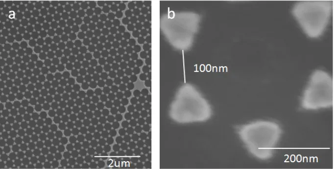
Initially, bowties were patterned by nanosphere lithography, which utilizes the
voids formed between the close-packed polymer beads to make triangular patterns9.
Polystyrene nanospheres were dispersed on silicon substrate followed by 30 nm-thick Ag
and 5 nm SiO2 interlayer deposition by e-beam evaporation and atomic layer deposition
(ALD), respectively (Methods and Fig. 2.4). The separation between tips of the triangles
was 200 nm (Fig. 2.3e).
Figure 2.4 | a, Schematic of metal-dielectric bowties on silicon substrate. b, Diagram of
nanosphere lithography. Reprinted with permission from ref. 9. © 1995, American
17
In order to achieve concentration of E-field inside the bowtie gap from the
lightning rod effect, the gaps between the bowties needed to be much closer, around a
few tens of nanometers. Thus, to achieve smaller gap separation between the triangles,
oxygen plasma was utilized to melt the surface of the PS nanospheres and fill in the
voids. Resulting bowtie structures following the SiO2 interlayer and metal deposition
shows much closer gap of 100 nm (Fig. 2.5a,b).
Figure 2.5 | a-b, SEM images of bowtie structures after O2 plasma etching of the PS nanospheres and deposition of metal (30 nm Au) and interlayer oxide (5 nm SiO2).
Nanosphere lithography has a few limitations; metals thicker than the diameter of
the nanospheres cannot be deposited due to difficulty in lift-off. This limits the study of
thickness-dependent surface plasmon (SP) mode. Usage of larger diameter nanospheres,
however, increases the gap separation. Also, the triangles will always have rounded tips
that result from melting of the PS beads. In order to realize high concentration of E-field
inside the bowtie gap, the tips need to be sharper. Moreover, there may be residue from
18
controllable method, electron beam lithography (EBL), was chosen to fabricate metal
bowties.
For optimization of bowtie patterns via EBL, various parameters and conditions
relating to the lithography process were tested. After trial and error, the beam current was
fixed at 500 uC/cm2 and the exposure time was varied in a range to optimize the shape of
the bowties. Figure 2.6 shows the SEM images of underexposed, overexposed, and
optimized bowtie shape.
Figure 2.6 | Schematic of bowtie array with gap separation, g, and side length, s. SEM example image of an underexposed (a), overexposed (b), and optimized (c) silver bowtie.
2.4.2 Plasmon resonances in bowtie array
50 nm-thick silver bowtie arrays with varying geometrical factors were patterned
on SiO2/Si substrate via electron-beam lithography (Methods and Fig. 2.7a). Silver was
used due to its strong plasmonic resonances as well as relatively low dissipation in the
19
numerical calculations were carried out by finite-difference time-domain (FDTD) method
(Methods). The calculated extinction cross-sections of a single bowtie (g = 20 nm, s =
100 nm) on a 300 nm SiO2/Si substrate for both TE (E-field parallel to the bowtie axis)
and TM (E-field perpendicular to the bowtie axis) polarizations are shown in Fig. 2.7b.
The TE polarized LSP mode was obtained at 2.16 eV while the TM polarized LSP mode
was located at a higher energy (2.5 eV) due to a stronger restoring force of the charge
oscillation. Both LSP modes are very broad with ~0.4 eV linewidth, spanning most of the
visible region of the electromagnetic spectrum. However, when the bowties are
periodically patterned into a 2-D array, a new type of lattice-coupled LSP (lattice-LSP)
resonances is produced with narrow resonance linewidths4-6,7,10. As expected from the
discussion in Background section, this is due to the coherent coupling between the
bowtie’s LSPs and the grating modes created by periodic array. For example, the
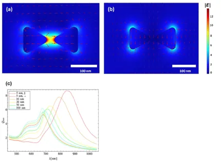
calculated quality factor (Q) of a lattice-LSP resonance at 1.9 eV (Fig. 2.7c, green curve)
is 21, in comparison to a Q of 6 for a single-bowtie LSP resonance (TE, Fig. 2.7b).
Furthermore, mode tunability of lattice-LSP resonances improves significantly compared
to single bowtie LSPs, as represented in the calculated E-field enhancement profiles in
Fig. 2.7c. Spatial E-field profiles (insets in Fig. 2.7b,c) show that the plasmonic fields are
mostly concentrated between the gaps or tips of the bowties with small optical mode
20
Figure 2.7 | a, Device schematic indicating the geometrical factors of a bowtie array: gap separation (g), side length of a triangle (s), and unit cell dimension or pitch (p = (px, py)).
b, Calculated extinction of a single bowtie (g = 20 nm, s = 100 nm) with the inset
displaying the E-field intensity profiles for TE and TM polarizations with respect to the
long axis of a bowtie. c, Calculated E-field enhancements in the array of bowties (s = 100
nm) with four different unit cell lengths (p). Inset shows the E-field intensity profiles for
TE or TM polarizations. Reprinted with permission from ref. 10. © 2015, American
Chemical Society.
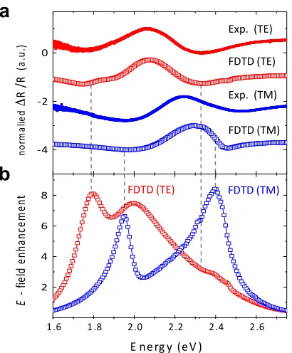
Polarization-dependent reflectance measurements were performed on a bowtie
array in order to resolve the lattice-LSP modes. The differential reflectance (ΔR/R =
(Rsample ‒ Rbackground)/Rbackground) spectra measured in TE and TM polarizations show two
broad dips for each polarization (Fig. 2.8a, solid curves). These are also in good
agreement with the calculated differential reflectance (Fig. 2.8a, open circles).
Comparison of the calculated E-field enhancement profiles and the corresponding ΔR/R
profiles reveals that the lattice-LSP modes, which correspond to the peaks of the E-field
enhancement spectra, are near the dips of ΔR/R (Fig. 2.8a,b). Thus, the lattice-LSP modes
of bowtie arrays can be related to dips in the reflectance spectra. More comprehensive
understanding of how the dips in ΔR/R relate to E-field enhancement is provided in Fig.
21
modes for TM polarization are located at higher energies compared to TE due to a
stronger restoring force of the charge oscillation in the direction of the bowtie axis.
Figure 2.8 | Polarization-dependent reflection spectra of the bowtie resonator array.
a, Normalized differential reflectivity (ΔR/R) spectra of experimental and calculated
lattice-LSP modes in TE and TM polarizations for bowtie array on SiO2/Si substrate.
Geometrical factors: s = 100 nm, g = 20 nm, p = (500 nm, 300 nm). b, Average E-field
enhancements for bowtie array on SiO2/Si calculated for the total area of the unit cell. Reprinted with permission from ref. 10. © 2015, American Chemical Society.
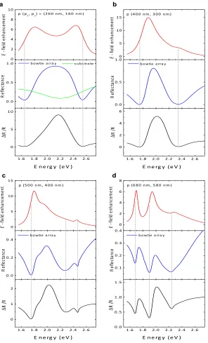
Figure 2.9 shows the relationship between E-field enhancement and reflectance.
The calculated E-field enhancement in bowtie arrays corresponds to the location of
lattice-LSP modes (red curves). Since lattice-LSP modes are a coupled system between
individual bowtie LSPs and lattice modes, the reflection spectra are affected by both the
superradiant LSP dipole modes and subradiant lattice (grating) modes due to radiation
1.6 1.8 2.0 2.2 2.4 2.6
0 1 2 3
2.26 2.28 2.30
0.0 0.5 1.0 1.5 * In te n si ty *( x1 0 5) E1 2g A1g Bex Aex
E nerg y*(eV )
In te n si ty *( x1 0 5 ) * *
E nerg y*(eV )
;4 ;2 0 * no rm al ie d * Δ * R */ * R * (a .u .) * * 2 4 6 8 * E *;* fie ld *e nh an ce m en t * Exp.**(TE) FDTD*(TE) Exp.**(TM) FDTD*(TM) FDTD*(TE) FDTD*(TM) Exp.**(TE) Exp.**(TM)
a
b
c
d
e
HorizontalBowties.(TM) VerticalBowties.(TE)
MoS2
Raman Aexciton
5 30 20 10 E !
1.6 1.8 2.0 2.2 2.4 2.6
0 1 2 3
2.26 2.28 2.30
0.0 0.5 1.0 1.5 * In te n si ty *( x1 0 5)
E12g A1g
Bex Aex
E nerg y*(eV )
In te n si ty *( x1 0 5 ) * *
E nerg y*(eV )
;4 ;2 0 * no rm al ie d * Δ * R */ * R * (a .u .) * * 2 4 6 8 * E *;* fie ld *e nh an ce m en t * Exp.**(TE) FDTD*(TE) Exp.**(TM) FDTD*(TM) FDTD*(TE) FDTD*(TM) Exp.**(TE) Exp.**(TM)
a
b
c
d
e
HorizontalBowties.(TM) VerticalBowties.(TE)
MoS2
Raman Aexciton
22
progress in the plane of the bowtie array for normal excitation. In addition, a 300 nm
thick SiO2/Si substrate produces a broad reflection signal as a background (Fig. 2.9a,
green curve). Therefore, the reflection spectra of the bowtie arrays are mainly composed
of all these factors: the broad reflectance of 300 nm thick SiO2/Si substrate, the
backscattered signal from superradiant LSP dipole mode, and surface-propagating signals
from the lattice modes. These signals interfere and result in the complex reflectance and
∆R/R spectra (Fig. 2.9, blue and black curves). The peaks of E-field enhancement spectra
are located near the dips of the reflectance spectra. The lattice-LSP mode positions are
thus near the dips in the reflection spectra, which is consistent in all four samples with
23
Figure 2.9 | Calculated average E-field enhancement, reflectance (ratio of reflected light
to incident light intensity), and ∆R/R spectra for the bowtie arrays on SiO2/Si substrate
with different pitch values (a-d). ∆R/R shows enhanced features due to subtraction of the
background. Bowtie geometrical factors: g = 10 nm, h = 50 nm, s = 100 nm. Reprinted with permission from ref. 10. © 2015, American Chemical Society.
0 2 4 6 8 1 0 E -‐ fie ld e nh an ce m en t
p (px, py) = (2 6 0 nm , 1 6 0 nm )
0 .0 0 .5
1 .0 bowtie a rra y s ubs tra te
Re fle ct an ce
1 .6 1 .8 2 .0 2 .2 2 .4 2 .6 0 5 1 0 Δ R / R
E ne rg y (e V )
a 0 .0 0 .5 1 .0 Re fle ct an ce
bowtie a rra y
1 .6 1 .8 2 .0 2 .2 2 .4 2 .6 0 2 4 6 Δ R / R
E ne rg y (e V )
0
5 1 0
1 5 p (4 0 0 nm , 3 0 0 nm )
E -‐ fie ld e nh an ce m en t b 0 5 1 0 1 5
p (5 0 0 nm , 4 0 0 nm )
E -‐ fie ld e nh an ce m en t 0 .0 0 .2
0 .4 bowtie a rra y
Re fle ct an ce
1 .6 1 .8 2 .0 2 .2 2 .4 2 .6 0 1 2 Δ R / R
E ne rg y (e V )
c 0 2 4 6 8
p (6 8 0 nm , 5 8 0 nm )
E -‐ fie ld e nh an ce m en t 0 .1 0 .2 0 .3 0 .4
bowtie a rra y
Re fle ct an ce
1 .6 1 .8 2 .0 2 .2 2 .4 2 .6 0 .0 0 .5 1 .0 1 .5 Δ R / R
E ne rg y (e V )
24
In order to investigate how the lattice-LSP modes change as the distance between
bowties are varied, pitch-variation study was performed. Five bowtie arrays with
different pitches (Fig. 2.10b, A-E) were fabricated on a SiO2/Si substrate under same
lithography conditions. The reflectance spectra show that for both polarizations, the dip,
or mode as the two are closely related (Fig. 2.8, 2.9), is close to a single dip at the largest
pitch (blue curves, sample E). When bowties are separated far away from each other, they
can be thought of as a single, uncoupled bowtie. Thus, this is consistent with the result in
Fig. 2.7b which shows a single broad mode for each polarization. Also, note that the
modes are generally located at higher energies for TM polarization, consistent with Fig.
2.8. As the pitch decreases and bowties are brought closer to each other, the positions of