Reverse Engineering Digital Circuits Using
Structural and Functional Analyses
Pramod Subramanyan, Nestan Tsiskaridze, Wenchao Li, Adri `a Gasc ´on,
Wei Yang Tan, Ashish Tiwari, Natarajan Shankar, Sanjit A. Seshia and Sharad Malik
!
Abstract—Integrated circuits (ICs) are now designed and fabricated in a globalized multi-vendor environment making them vulnerable to malicious design changes, the insertion of hardware trojans/malware and intellectual property (IP) theft. Algorithmic reverse engineering of digital circuits can mitigate these concerns by enabling analysts to detect malicious hardware, verify the integrity of ICs and detect IP violations.
In this paper, we present a set of algorithms for the reverse engineer-ing of digital circuits startengineer-ing from an unstructured netlist and resultengineer-ing in a high-level netlist with components such as register files, counters, adders and subtractors. Our techniques require no manual intervention and experiments show that they determine the functionality of more than 45% and up to 93% of the gates in each of the test circuits that we examine. We also demonstrate that our algorithms are scalable to real designs by experimenting with a very large, highly-optimized system-on-chip (SoC) design with over 375,000 combinational elements. Our inference algorithms cover 68% of the gates in this SoC. We also demonstrate that our algorithms are effective in aiding a human analyst detect hardware trojans in an unstructured netlist.
1
INTRODUCTION
Contemporary integrated circuits (ICs) are designed and fab-ricated in a globalized, multi-vendor environment due to which ICs are vulnerable to malicious design changes and the insertion of hardware trojans and malware. The possibility that malicious chips might be used in sensitive locations such as military, financial and government infrastructure is a serious and pressing concern to both the users and design-ers of contemporary ICs [8, 15, 28, 1, 17]. For example, the DARPA IRIS program seeks to develop techniques for reverse engineering digital, analog and mixed-signal ICs to determine their integrity for use in sensitive installations [5]. Algorithmic approaches to reverse engineering chips can aid in the detection of hardware trojans, malicious design changes • Pramod Subramanyan, Nestan Tsiskaridze and Sharad Malik are with the Department of Electrical Engineering, Princeton University. E-mail: [email protected], [email protected] and [email protected].
• Wenchao Li, Wei Yang Tan and Sanjit A. Seshia are with the Depart-ment of Electrical Engineering and Computer Sciences, UC Berkeley. E-mail: [email protected], [email protected] and [email protected].
• Adri`a Gasc´on, Ashish Tiwari and Natarajan Shankar are with the Computer Science Laboratory, SRI International. E-mail: [email protected], [email protected] and [email protected].
and in verifying the integrity of untrusted design components for which trustworthy source code may not be available. Reverse engineering is also important in detecting intellectual property violations, considered a “serious concern” for the semiconductor industry [7].
In this paper, we study a portfolio of fully algorithmic approaches to reverse engineer digital circuits. We analyze an unstructured netlist with the objective of inferring a high-level netlist with components such as register files, adders and counters. The key challenge in analyzing an unstructured netlist is that we have no information about the boundaries of the modules contained in the netlist. Therefore, we tackle the reverse engineering problem through a variety of algo-rithms that “carve out” portions of the netlist to generate potential/candidate modulesand employ techniques similar to those used in design synthesis and verification to determine the functionality of these modules. In particular, this paper focuses on algorithmic reverse engineering ofdatapathcomponents in an unstructured netlist. The objective is to aid a human analyst understand the functionality of an unstructured netlist by algorithmically identifying as many components as possible.1
1.1 Related Work
Fully algorithmic reverse engineering is a relatively new field of research. Previous work primarily suggests strategies of attack for a human analyst [9, 29]. For example, in their investigation of the ISCAS ’85 benchmarks, Hansen et al. analyze replicated structurally isomorphic blocks [9]. The cut-based Boolean matching and aggregation algorithms presented in§2.1 and §2.2 are generalizations of this idea.
A recent attempt at addressing the reverse engineering prob-lem algorithmically is by Li et al. [14]. They present a method for behavioral matching of an unknown sub-circuit against a library of abstract components but assume that methods are available to generate sub-circuits from the unstructured netlist. Therefore, our set of solutions is complementary to theirs because: (a) we target different kinds of components for reverse engineering and (b) we analyze an unstructured netlist as opposed to sub-circuit matching.
1. Note that 100% identification will not be possible because of the focus on datapath components. This is not a serious limitation as discussed in§5.4 and§6.
An alternative approach to malware detection relies on comparing side channel signals such as power and timing between the trusted design and untrusted versions of the designs. For instance, Agrawal et al. compare “fingerprints” consisting of measurements of power, electromagnetic and thermal emissions [2]. Wang et al. use differences in current measurements to detect trojans [31]. Jin et al. compare path delay measurements [11]. These approaches assume that a trusted (”known good”) version of the chip is available for experimentation, something that may not be true when un-trusted component IPs are used, the foundry itself is unun-trusted or when it is not possible to determine trustworthy chips by destructive examination.
Architectural approaches to trojan detection and avoidance have also been proposed. Hicks et al. [10] proposed an analysis that detects pairs of circuit nodes that are not exercised by design verification tests. They suggested that these nodes could potentially be used to hide trojans and proposed an architec-tural technique that eliminates such nodes from the circuit and emulates their designed functionality through software.2
Waksman et al. [30] proposed a set of transformations that permute module inputs, the order in which inputs are applied, and obfuscate reset sequences in order to prevent Trojan activation. Both proposals assume availability of RTL source and design verification tests for the design being analysed.
Trojan detection through algorithmic reverse engineering does not rely on any of these assumptions. Hence, it can detect a wider range of malware, including, for example, bugs/malware introduced by design automation tools. This additional coverage comes at a cost, which is that traditionally reverse engineering has been a labor-intensive process. We show that fully algorithmic reverse engineering is both feasible and effective even for very large designs. A comparison of the differences in assumptions of availability and threat models for the techniques discussed above is shown in Table 1.
This paper builds upon our past work in the area of algorithmic reverse engineering in [26] and [13]. A detailed discussion of the differences between these past efforts and this paper is deferred to Section 6.2.5. The problem of deriving a gate-level netlist from a physical chip is outside the scope of this work. This has been studied in [29, 19, 27, 20, 12]. Nohl et al. derive a gate-level netlist of an RFID tag and examine it for cryptographic vulnerabilities [20]. K¨ommerling et al.describe techniques for obtaining gate-level descriptions of smartcard processors [12]. Tarnovsky used electron microscopy and bus-level probing to reverse engineer an Secure Infineon Processor which included mesh shielding inserted in order to thwart reverse engineering [27] .
1.2 Solution Overview
In this subsection, we describe the assumptions and objectives underlying this work and then provide an overview of our solution.
2. We note that this technique has been defeated [24].
1.2.1 Assumptions
We tackle the problem of reverse engineering a gate-level netlist under the following assumptions. First, we assume that register transfer language (RTL) source code for the test article being analyzed is not available. We also assume that micro-architectural information as well as design-specific information pertaining to the test article being analyzed is also
notavailable. We only assume availability of “datasheet-level” information which usually consists of a high-level description of the functionality of the test article and a description of its input/output pin interface.
1.2.2 Objective
Given these assumptions our target is to algorithmically derive information about high-level components present in the test article by analyzing the gate-level netlist.
1.2.3 Discussion of Assumptions and Objectives
In both the (a) trojan-detection and (b) intellectual property infringement usage scenarios, our assumptions correspond to an external analyst examining a test article to determine if it (a) contains hardware trojans or (b) infringes relevant intellectual property. Note that the analyst does not have access to source code for the design. Therefore, traditional techniques for trojan detection [2, 31, 11] are not applicable. Furthermore, the only plausible alternative to algorithmically assisted reverse engineering is full manual inspection of the netlist.
In case the assumptions for trojan detection scenario are weaker than ours, we note that our techniques are complemen-tary to the other trojan detection techniques discussed in the previous section. For example, when considering the threat of trojans inserted in the RTL or by design automation tools, anal-ysis techniques like UCI [10] can be synergistically applied along with algorithmic reverse engineering of the gate-level synthesized netlist and correlating identified components with those expected to be present. Note UCI itself cannot detect trojans inserted by design automation tools. Furthermore, all techniques studied in this paper rely on a “static” analysis of the netlist and do not consider information derived from sim-ulations. Combining these algorithms with simulation-based “dynamic” analysis techniques will likely yield interesting results because these approaches are complementary.
Our algorithms focus on identifying datapath components. The are three reasons for this design choice. First, any attack model that is based on triggering malicious behavior through a rare input sequence will necessarily involve some manipulation of the datapath. In fact, as illustrated in§5.4, it is likely that this malicious logic will manifest as a collection of datapath components such as counters, decoders and multiplexers. Thus identifying such components will help an analyst quickly zero-in on problematic parts of the netlist. Second, datapath components exhibit regularity and structure and are amenable to algorithmic analysis. Finally, the majority of the gates in processor-like circuits are in the datapath. The focus on datapath components means that it will not be possible to reverse-engineer 100% of the gates in the design. However, as will be shown in §5.4, this is not a major limitation for detecting hardware trojans.
TABLE 1
Comparing Techniques for Trojan Detection With This Work.
Detection Technique Trojan Threat Model Availability Assump-tions
Automation Paper Description
Side-channel analysis Malicious foundry Known good chips full
Agrawal et al. [2] Statistical comparison of power measurements with good chips. Jin et al. [11] Statistical comparison of path delays with good chips. Wang et al. [31] Statistical comparison of current measures with good chips. RTL and test case analysis Malicious RTL RTL source, design verification tests
partial Hicks et al. [10] Identify and eliminate circuit nodes never exercised by verifica-tion tests.
partial Waksman et al. [30]
Obfuscate inputs, time order of inputs and reset sequences to prevent trojan activation.
Algorithmic reverse engineering Malicious RTL, design tools, foundry Gate-level
netlist partial This work. Algorithmic reverse engineering followed by manual analysis.
It is important to note that this work develops a set of algo-rithms thataidtrojan detection. By providing a human analyst with an abstracted netlist containing high-level components, it makes the job of the analyst much easier than if the analyst were to individually examine hundreds and thousands of gates and latches. The tool itself does notperform trojan detection.
1.2.4 Solution
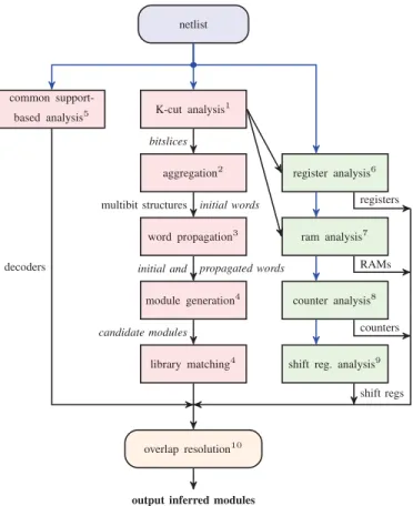
The objective of our work is to infer a useful high-level description from an unstructured gate-level netlist. In partic-ular, we focus on reverse engineering datapath elements in digital circuits. Even when focusing primarily on the datapath, reverse engineering is still a very hard problem because we are starting with a sea of gates for the complete chip, including the datapath as well as the control logic, and it is not obvious how to go about finding some meaningful subset of the gates/latches for algorithmic analysis. Hence, our approach integrates a number of different techniques tackling different aspects of the problem. Figure 1 shows the techniques we introduce and their inter-relationships.
Our strategy is to attack the problem in two stages. The first stage identifies potential module boundaries using topologi-cal/functional analyses. The second stagefunctionally analyzes potential modules to understand their behavior.
The reverse engineering algorithms introduced by this paper are as follows:
1) We present a novel application of cut-based Boolean matching to find replicated bitslices3 in the netlist. This
analysis helps us find circuit nodes that correspond to functions such as 1-bit adders and 1-bit multiplexers. 2) We present algorithms that topologically analyze the
results of bitslice matching to aggregate multibit com-ponents such as multiplexers, adders and subtractors. 3) Analyzing aggregated modules helps identify bits which
are operated upon simultaneously, allowing us to infer
words. These inferred words are then used in our word propagation algorithm to generate additional words. 4) Our module generation algorithm analyzes words which
are structurally connected to generatecandidate unknown
3. We define a bitslice as a Boolean function with one output and a small number of inputs that is replicated to construct multibit datapath operators.
netlist K-cut analysis1 aggregation2 word propagation3 module generation4 library matching4 common support-based analysis5 register analysis6 ram analysis7 counter analysis8
shift reg. analysis9
overlap resolution10 bitslices
multibit structures initial words
initial and propagated words
candidate modules registers RAMs counters shift regs decoders
output inferred modules
Fig. 1. Portfolio of the reverse engineering techniques introduced in this paper. Superscripts refer to items in our list of reverse engineering algorithms introduced by this work. Algorithms 1-5 identify combinational modules while algorithms 6-9 identify sequential modules.
modules. These are potential operators with word argu-ments and results and are matched against a component library using a Quantified Boolean Formula (QBF) for-mulation.
5) We present an alternate strategy to infer combinational modules like decoders using a BDD-based analysis of nodes with common inputs.
6,7) We present novel algorithms that identify word-level registers, as well register array structures like register files
and RAM arrays using a BDD-based functional analysis. 8,9) We present algorithms to identify counters and shift registers using topological analyses combined with a satisfiability (SAT) checking formulation.
10) Modules inferred by the above-mentioned portfolio of algorithms may “overlap”, i.e., cover the same elements.4 These overlaps are resolved by formulating an integer lin-ear program (ILP) that selects a non-overlapping subset of inferred modules that optimizes a set of desired metrics.
TABLE 2
Netlists Used in Experiments. Design Chip Chip Gates Latches Notes
Inputs Outputs Flip-flops
router 35 26 896 182 on-chip router
eVoter 31 15 1360 108 voting machine [25]
Open8† 19 26 1807 237 Open CPU
cpu8080† 12 29 2258 243 8080 CPU
ae18† 32 64 3466 1094 ae18 CPU
MIPS16† 1 8 6986 4380 16b MIPS-like core
oc8051† 86 78 8164 2748 8051μcontroller
RISC FPU 35 66 14291 3097 RISC FPU
The contributions of this paper include the reverse engi-neering algorithms listed above as well as the analysis flow shown in Figure 1. We also present a detailed evaluation of our algorithms by experimenting with eight unstructured netlists, details of which are shown in Table 2. The netlists marked with a dagger (†) were obtained by synthesizing designs from opencores.org. Results show that our inference algorithms determine the functionality of more than 45% and up to 93% of gates in the designs in a fully automated manner.
Furthermore, we present a case study of algorithmic reverse engineering of a large highly-optimized system-on-chip (SoC) design consisting of over 375,000 combinational elements. We show a large design like this can be analyzed through logic simplification and module partitioning. Our results show that 68% of the gates left after simplification in this SoC were covered by our inference algorithms. We believe our work is the first effort to algorithmically reverse engineer the majority of the gates in a design of this scale.
A final important contribution of our work is a case study of how our algorithms could aid the detection of hardware trojans. We inject trojans into two test articles and discuss how algorithmic reverse engineering helps a human analyst detect this malicious circuitry.
The rest of this paper is organized as follows. Section 2 describes our algorithms for identifying combinational com-ponents. Section 3 describes our algorithms for identifying sequential components. Section 4 describes how possibly conflicting inference results from different algorithms can be resolved to produce the final set of inferred modules. Section 5 presents the experimental evaluation of these algorithms. Sec-tion 6 discusses limitaSec-tions and avenues for further analysis. Section 7 provides some concluding remarks.
4. We use the term element to refer to gates, latches and other circuit nodes in the input netlist.
2
IDENTIFYING
COMBINATIONAL
MODULES
The section describes algorithms to identify fully combina-tional modules. Our first algorithm is based on the observation that many datapath elements consist of replicated bitslices connected in a specific topology and is described in §2.1 and §2.2. We then present algorithms for identifying word-level modules in§2.3 and§2.4. Finally, §2.5 presents a third attack on combinational modules using a specific topological property.2.1 Bitslice Identification
The goal of bitslice identification is to identify all nodes in the circuit that match functions from a bitslice library. For instance, we might be interested in finding all nodes that match the full adder carry functionf(a, b, c) =ab+bc+ca, this might help identify multibit adders. We adopt afunctionalmatching approach, which matches based on the function implemented by a set of gates instead of matching structural patterns. This uses cut-enumeration and Boolean matching, which was initially introduced for technology mapping [4, 3].
A feasible cut of a circuit node G is defined as a set of nodes in the transitive fan-in cone ofGsuch that a consistent assignment of truth values to each node in the set completely determines the value of G [3]. A cut is said to bek-feasible
if it has no more thankinputs. The trivial cut{G}is always
k-feasible. The set ofk-feasible cuts for a gate is recursively computed by enumerating the union of all k-feasible cuts of the gate’s inputs such that this union haskor fewer inputs.
Our tool enumerates all 6-feasible cuts. We found that the average number of 6-feasible cuts per gate is between 15 and 35. The number of cuts for k > 6 is significantly higher.5 Although we are restricted to bitslices with six or fewer inputs, this is not a major limitation as most common bitslices have less than six inputs; e.g., a full adder bitslice has 3 inputs.
Once all cuts are identified, they are grouped into equiva-lence classes using permutation-independent Boolean match-ing. For example, nodes matching the function f(a, b, c) = ab+cand nodes matchingf(a, b, c) =bc+aare grouped into the same class. Each equivalence class may match a known library function.
2.2 Aggregation to Multibit Components
Now that we have all the nodes that match a particular function, the next step is to look for matching nodes connected in interesting patterns.Aggregating replicated bitslices which are connected in specific patterns is our first technique for identifying combinational modules. The following subsections expand on our aggregation algorithms.
2.2.1 Common Signals in Replicated Bitslice
This algorithm considers all bitslices that match a particular function and groups them using common input signals. For instance, consider the function that represents a 2:1 multi-plexer: f(a, b, s) = sa+¬sb. Here we group all matching 5. These results are in line with published work on cut enumeration [3].
bitslices which have a common6 select signal (s in this
example). Common signal aggregation finds 59 decoders and 140 multiplexers in the RISC FPU test article.
Besides aggregating functions in the bitslice library such as multiplexers and decoders, we can also aggregate unknown functions connected by a common signal to generate candidate unknown modules. These modules may be analyzed either by a human analyst or by a permutation and phase independent matching algorithm such as [18].
2.2.2 Propagated Signal(s) in Replicated Bitslices
In this case, the algorithm considers all bitslices matching a particular function such that the output of one bitslice is the input of another (e.g., carry chain in a ripple carry, parity tree). Propagated signal aggregation finds 37 adders/subtractors and 10 parity trees in the RISC FPUtest article.
2.3 Word Identification and Word Propagation Aggregated bitslices tell us about circuit nodes that are oper-ated upon simultaneously. These nodes are likely to form part of sameword. Our tool groups the bits that are inputs/outputs of aggregated modules into “word” data structures.
2.3.1 Symbolic Word Propagation
Once some words are identified, more words can be generated by propagating them across gates. The idea is, given a word
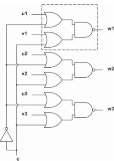
w, find conditions under which its value is propagated to a new word w, for every possible value of w.
Consider the circuit in Figure 2. Note that the circuit behaves as a selector between the bitwise negation of the wordu1, u2, u3and the bitwise negation of the wordv1, v2, v3
depending on the value of c. Hence, the negated value of
u1, u2, u3 gets propagated to w1, w2, w2 if c = 0, and the negated value of u1, u2, u3 gets propagated to w1, w2, w2, otherwise. These are the kind of claims produced by the word propagation algorithm.
For efficiency reasons, we use symbolic simulation, which allows consideration of all possible values of w simultane-ously in a single run. Similar to Roth’s D-calculus [22], we redefine functions of logic gates in the circuit operating on the expanded domain {0,1, D,D, X¯ }, whereD represents a symbolic value in {0,1}, D¯ is the negation of D, and X
represents an unknown value. Some examples of symbolic evaluation are:and(D,1) =D,and(D,0) = 0,and(0, X) =
0,not(X) =X, andnot(D) = ¯D.
Our word propagation algorithm follows a “guess and check” approach. Given an initial word w, the guessing stage consists on finding a setS of potential “target words” for the propagation. Such setS is computed by grouping the outputs of the gates driven by the signals in w by gate type and port they connect to. Then, for each target word w ∈S, a set C
of control wiresis computed as the set of wires lying in the intersection of the fanins (up to a small depthk) of the gates whose output is inw. The checking stage consists on running several symbolic simulations of the local netlist that is relevant 6. A simple structural analysis is used to find functionally equivalent nodes.
Fig. 2. Example: Word propagation
to the propagation that is being checked. In such simulations, the inputs of such local netlist are initialized as follows.
• Each bit ofwis set to the symbolic value D.
• For each combination of 3 wires taken from the set of all control wires, all possible binary values are evaluated.
• The rest of the inputs of the local netlist are assignedX. A simulation with a particular partial assignment σ to the control wires succeeds if all wires in the target word evaluate to either D or D¯. In that case, w propagates to w under σ
andw can be tested for further propagation.
An analogous approach in which w is guessed among the structural predecessors ofwand it is checked whetherw can be propagated towallows to test forbackward propagation. 2.4 Module Identification and Matching
The two main limitations of bitslice identification are: (i) we are limited to bitslices with a maximum of 6 inputs due to thek≤6limitation on cut-enumeration and (ii) it is difficult to identify combinational structures that do not have a clean interconnection pattern. Our second approach overcomes these limitations by constructing entire modules and then matching them against a component library.
The intuition here is that since datapath circuits operate on word inputs and produce word outputs, cutting out portions of the circuit that existbetween wordsmay find interesting can-didate modules. Our module identification algorithm identifies combinatorialcandidate unknown modulesoperating on words and checks equivalence against a set of predefined reference modules implementing common operations such as addition, subtraction, boolean operations, and shifting/rotation.
For example, consider words w1, w2, w, and the largest combinatorial sub-circuitC having w1 andw2 as inputs and
w as output. Additionally, C may have additional inputs, to which we refer asside inputs. LetY be the set of all side inputs of C. Due to optimizations introduced during the synthesis process or simply a design decision, the function implemented by C might not be unique since the values of some of the wires in Y determine the operation implemented by C, e.g, addition or subtraction. For this reason, given a reference
module C we model our equivalence checking as a 2QBF7
satisfiability question: is there any value for the wires in Y
such that, for every value of the inputs w1, w2, C and C
give the same output? More concretely, we construct a miter formula Φ(X, Y) from C and C by inserting a comparator between their respective outputs. Then, using a state-of-the-art QBF solver, we find values for the side inputs inY forC to match the function implemented by C.
Reference Circuit = module Y side inputs X Φ ∃Y∀XΦ(X, Y)
Fig. 3. QBF formulation showing Miter construction. The module matching algorithm was able to identify the 8-bit ALU performing addition, subtraction, rotation and nega-tion in theoc8051test article. Each operation is performed for a different setting of the side inputs, so this module cannot be detected through bitslice aggregation. The ability to create and identify word-level modules was key here.
2.5 Analyses Based on Common Support
In this section we introduce an algorithm that detects modules that do not necessarily have word inputs or outputs or consist of small replicated bitslices. This analysis technique can be used to detect combinational modules with the specific property that each of the outputs of the module depend on the same set of inputs.
Examples of modules which satisfy this property are de-coders, demultiplexers and population counters. Note that modules like adders and multipliers do not satisfy this prop-erty. Output bit 0 of an adder only depends on the two least significant bits of the addend and the augend, while output bit
k of the adder depends on the k least significant bits of the addend and the augend respectively.
2.5.1 Identifying Output Nodes with Identical Supports
Consider the full combinational fanin cone of a combinational node in the circuit. The inputs of this cone are the chip inputs and latch outputs. Suppose two combinational nodes in the circuit are computed using the same set of circuit nodes, it is clear that the inputs of the full combinational fanin cone of these nodes will also be the same.
Therefore, we can group nodes into equivalence classes in the following way. Two nodes are placed in the same class iff the inputs of their full combinational fanin cones are the same. These equivalence classes can computed efficiently using a union-find data structure and give us candidate output nodes with the property that they are fully determined by the same set of inputs.
7. 2QBF is the problem of evaluating a Quantified Boolean Formula (QBF) with two levels of quantification [21].
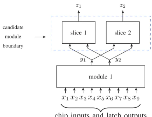
module 1 x1x2x3x4x5x6x7x8x9 slice 1 z1 slice 2 z2 candidate module boundary y2 y1
chip inputs and latch outputs Fig. 4. Nodes with common support.
Consider the example shown in Figure 4. Nodesz1 andz2
will be grouped in the same equivalence class because they are completely determined by the same set of chip inputs and latches: x1 . . . x9. Such nodes (z1 and z2) will form the outputs of the candidate module.
However, to determine the module boundary we still need to find the inputs of the module, i.e., nodes y1 and y2 in Figure 4. The module boundary is given by the set of nodes in the full combinational fanin cone of the candidate outputs which arenot presentin the intersection of each of these fanin cones. It is visually clear from the figure that intersection of the combinational fanin cones contains only module 1, so the nodes in the fanin cone which are not present in the intersection leaves us with correct module boundary.
2.5.2 Verifying Module Properties
We use a BDD-based formulation to verify the properties of the modules generated by the algorithm in §2.5.1.
To verify whether a potential module is a decoder or demultiplexer, all that needs to be done is to prove that each output is satisfiable and that no two outputs of the module are simultaneously high.8This can be verified in a straightforward
manner using a BDD-based analysis.
A population counter can be detected using a similar algorithm which uses BDD-based matching to compare the function of each output node against the function representing each output bit of a population counter.9
2.6 Post-Processing of Combinational Modules Modules generated by the inference algorithms described in this section are subject to a post-processing step that “fuses” certain types of modules to generate larger modules. This increases the level of abstraction of the inferred modules and makes the inference output easier to understand. For example, 2:1 muxes, 3:1 muxes and 4:1 muxes which are adjacent to each other are fused to form larger n:1 muxes. Similarly, 8. Assuming the decoder outputs are active-high. The case when the decoders outputs are negated is handled using a symmetric algorithm.
9. Although we verified that the population count algorithm works on artificially constructed circuits with popcnt modules in them, we could not find any population counters in the test circuits we experimented with.
decoders whose outputs drive the select inputs of muxes are fused with the muxes to form routing structures. Module types which can be fused in this manner are said to be compatible. Module fusion is performed by first constructing a module fusion graph. The nodes in the graph are modules and an edge between Module A and Module B exists in the graph if and only if all the outputs of module A are inputs of module B and respective module type are compatible. Once the module fusion graph is constructed, connected components in the graph are fused to form a larger combinational module and the resulting module is added to collection of inferred modules. The constituent modules which were the “inputs” of the fusion are not eliminated at this stage. The overlap elimination algorithm (see §4) determines which of these modules (fused vs. constituents) is included in the output.
3
IDENTIFYING
SEQUENTIAL
COMPONENTS
A reverse engineering solution must identify commonly occur-ring sequential components such as RAM arrays, register files, counters and shift registers because these cover a significant number of gates in circuits and also give insight into func-tionality of the circuit. The challenge here is again in finding meaningful module boundaries for these components given the unstructured netlist. Our strategy is to devise topological analyses to find circuit nodes that are potential counters, RAM outputs or shift registers. We then formulate functional analyses using SAT and BDDs that verify correctness of the “guess” made by the topological analysis. The rest of this section presents algorithms to identify RAM arrays/register files, counters, shift registers and multibit registers.3.1 Counter Identification
The specific problem in counter identification is to identify sets of latches in the unstructured netlist that behave like counters. The difficulty here is twofold. First, given a set of latches that we suspect to implement a counter, we need a functional analysis that can verify its properties. Second, we need an efficient algorithm to enumerate candidate counters. Simply considering all subsets of latches is computationally infeasible. Based on this observation, our analysis is performed in two stages. First, potential counters are generated by finding sets of latches whose interconnections match the counter topology shown in Figure 5. The intuition for this topology is that biti
of an-bit up counter toggles when the lower order bits1. . . i−
1 are all high. Therefore, there needs to be a combinational path from the outputs of these latches to the input of bit i, leading to the topology shown in the figure.
The next step uses a SAT-based functional analysis to verify whether the functions at the inputs of the latches in the counter satisfy the following conditions: (i) each latch toggles either when all the low-order latches are 1 (up counter) or all the low-order latches are 0 (down counter) and (ii) the conditions that control when the counter is enabled/reset are the same for all the bits of the counter.
3.1.1 Topological Check Using the LCG
The latch connection graph (LCG) is an unweighted graph
G= (V, E)which formalizes the notion of information flow between latches. The vertices of the graph (V) are the latches and flip-flops in the netlist being analyzed. A directed edge
(v1, v2)∈E iff there is a combinational path from the output of latchv1 (its Q node) to the input of latchv2 (its D node).
L0 L1 L2 L3 L4 L5
Fig. 5. Latch-to-latch information flow in a counter: each latch in the counter is driven by the latches corresponding to the lower-order bits.
Given the LCG, we find subgraphs which have the topology shown in Figure 5. More precisely, given the LCGG= (V, E), we find ordered sets of nodes Vc = {v1, . . . , vk}, such that Vc⊂V and∀vi, vj ∈Vc : (vi, vj)∈E iffi≤j.
3.1.2 Verifying Counter Properties
We now devise a functional analysis that verifies that the “candidate” counter found by the topological analysis has the properties of a counter. First, let us formalize the behavior of an up counter as follows.10
ci =¬r∧e∧(q1∧q2∧ · · · ∧qi−1)∧ ¬qi ∨
¬r∧e∧(¬q1∨ ¬q2∨ · · · ∨ ¬qi−1)∧qi ∨
¬r∧ ¬e∧qi ∨s (1)
In the equation above,ci determines the next state of biti
of an n-bit counter. r is the function that resets the counter,
sis the function that sets its value high,eis the count-enable function, andq1. . . qi are the current values of latches 1. . . i
of the counter.
Equation (1) says that bititoggles when all the lower order bits (1. . . i−1) are high, the counter is enabled and not being reset. The bit retains its value when the counter is enabled, not reset but one of the lower order bits is zero. The counter also holds its value when it is not reset and not enabled. Biti
is pulled high if the set function evaluates to 1. Note since we have left the functionsr,eandsunspecified,ci is actuallya family of functionsand not a specific Boolean function.
Now consider the Boolean function defined by the full combinational fanin cone for each latch in the candidate counter. Let this function be denoted by di where i ranges 10. For clarity of presentation the rest of this section focuses on up counters. Our implementation uses symmetric techniques to detect down counters.
across the bits of the counter. We compute the following cofactors from di.11
fi = cofactor(di, q1∧q1∧ · · · ∧qi−1∧ ¬qi) gi = cofactor(di, q1∧q1∧ · · · ∧qi−1∧qi) hi = cofactor(di,(¬q1∨ · · · ∨ ¬qi−1)∧qi)
The insight here is that if the functiondi is compliant with
ci from Equation (1), then the functions fi, gi and hi will reduce to Equation (2).
fi = (¬r∧e)∨s (2)
gi = (¬r∧ ¬e)∨s hi = ¬r∨s
Now, the functions r,s ande should be the same for all the bits in the counter. Hence, fi, gi and hi must also be equivalent. Therefore, we can determine that a set of latches is not a counter if the SAT solver finds that the functions fi,
gi andhi are not equivalent for all i.
Five counters were found in theoc8051test article. 3.2 Shift Register Identification
As with counters, our goal here is to identify sets of latches that form shift registers given an unstructured netlist. The shift register identification algorithm is similar to the counter identification algorithm in that it uses a topological check and a SAT formulation except that the topology and verification conditions differ.
3.2.1 Topological Check
The topological check for shift registers uses a pruned version of the latch connection graph (LCG) that we call the single path latch connection graph (SPLCG). As in the LCG, the nodes in the SPLCG are the latches and flip-flops in the netlist. However, the edge v1 →v2 exists in the SPLCG iff there is exactly one combinational path from the output of latch v1to the input of latch v2.
The topological check for unidirectional shift registers is as follows. Given the SPLCG G = (V, E), we find ordered sets of nodes Vs = {v1, v2, . . . , vk} such that Vs ⊂ V and ∀vi, vj ∈Vs: (vi, vj)∈E iffj =i+ 1. In other words, we are searching for chains of latches connected by exactly one combinational path between each latch and its successor.
3.2.2 Verifying Shift Register Properties
We model the family of functions representing the next-state function of bitiof a shift register using the following equation.
si=¬r∧(e∧qi−1∨ ¬e∧qi)∨s (3)
r, sandeare the reset, set and enable functions respectively.
qiis the output of theith latch of the shift register. Supposedi
is the Boolean function determined by the full combinational 11. Given Boolean functionsfandg,cofactor(f,g)is the function obtained whenfis evaluated over the restricted domain specified byg= 1.
fan-in cone of latchiof the supposed shift register. As in the counter analysis, we consider the following cofactors of di.
fi = cofactor(di, qi−1∧ ¬qi) gi = cofactor(di,¬qi−1∧qi)
Ifdi is complaint withsi we will have:
fi = ¬r∧e∨s gi = ¬r∧ ¬e∨s
Therefore, the functional check verifies that the functions
fi andgi are identical for each bit of the shift register.
3.2.3 Shift Register Aggregation
Shift registers may consist of multiple bits shifting in tandem from one set of latches to another. The basic algorithm finds each cascading chain of latches as separate shift registers. To aggregate shift registers, first we group shift registers by length. Next, we form equivalence classes within each group where shift registers with the same set, reset and shift-enable functions are classified together. Finally, each equivalence class is output as a multibit shift register module.
Seven shift registers were found in the RISC FPU test article.
3.3 Identifying RAMs
This section targets small RAM arrays and register files. Our objective here is to find the latches/flip-flops that form the RAM, associated logic that reads data (called “read-logic”) and logic that writes data into the latches (called “write-logic”).
3.3.1 Identifying Read Logic
The intuition behind identifying the read-logic is that it forms a set of trees with the RAM cells as leaves of the tree and the read outputs as roots. We use a marking algorithm to find such trees. Initially, the algorithm marks all latches in the netlist. Subsequently, it marks all gates which satisfy the following conditions: (i) at least one of the gate’s inputs is marked and (ii) the gate has only one fanout. This is repeated until no new nodes are marked.
3.3.2 Verification of Read Behavior
The next step is a functional analysis of the marked nodes. A BDD is constructed for each marked node in terms of the latches, inputs and unmarked nodes in the circuit. Among the inputs of this BDD, we assume that those which are latches are storage nodes (li) while the remaining are the read address (si). We then verify the following properties.
1) If y =f(s1, . . . , sk, l1, . . . , ln) then y = li or y =¬li
for every value of s1. . . sk. In other words, each select input propagates exactly one of the latches to the output. 2) Every latch node is propagated to the output: y =li or
y=¬li for alliand appropriate s1. . . sk.
Latches and nodes which pass these checks are identified as the RAM array and its corresponding read-logic.12
12. The analysis handles each bit output of the array independently so sets of latches with common select inputs (read addresses) are aggregated to form an array with multibit inputs/outputs.
3.3.3 Identifying Write Logic d q b a s d q b a s d q b a s we0 we1 wen wd0 wd1 wdn ...
Fig. 6. RAM write-logic:weiis the write-enable signal for wordiandwdiis the data to be written to wordi.
The logic that controls RAM writes is shown in Figure 6. It consists of decoders driving 2:1 muxes that select between the write-data and the latch output. The muxes drive the latch inputs and their select signal is the write-enable signal, denoted by wei. Once the latches that comprise the register file are known, cut matching can give us these muxes. Our algorithm then computes the BDDs for each write-enable signal using the intersection of combinational fan-in cones. The following properties are then verified: 13
1) Each write-enable signal is satisfiable: wei= 0.
2) No two write-enable signals are simultaneously satisfi-able: wei∧wej = 0if i=j.
If these properties are satisfied, the set of gates that com-prise the latch inputs, muxes and common support nodes are identified as the write-logic.14
One RAM structure, a 32x32b register file with two read ports and 1 write port, was detected in the RISC FPU. 3.4 Identifying Multibit Registers
We use the term multibit register to denote a set of 1-bit registers whose values are updated in tandem.
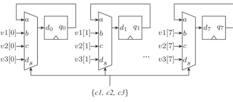
d0 q0 s a b v1[0] c v2[0] d v3[0] d1 q1 s a b v1[1] c v2[1] d v3[1] d7 q7 s a b v1[7] c v2[7] d v3[7] ... {c1, c2, c3}
Fig. 7. Register synthesis illustration.
One example of a multibit register is shown in Figure 7. Each cycle either one of three different values:v1[7 : 0], v2[7 :
0] or v3[7 : 0] or the current value of the registerq7. . . q0 is assigned to the register based on the conditions c1, c2 and
c3. A structure of this form can be detected using bitslice matching and aggregation to find the multibit multiplexer and 13. This presentation assumes the write-enable is signal is active high, but it could also be active-low in which case the properties are modified appro-priately. We determine the polarity of the write-enable signal by examining which of the mux inputs is connected to the latch output.
14. We note that the analysis is unable to determine the ordering of the bits in inputs and outputs of the RAM.
then examining the fanouts and inputs of the multiplexer to detect the sequential elements around it.15
39 multibit register elements were found in theRISC FPU.
4
OVERLAP
RESOLUTION
The inference algorithms described in this paper operate independently. Therefore, it is possible that a particular gate in the netlist under analysis might be placed in multiple inferred modules. For example, in theoc8051design, the RAM read-array consists of many muxes identified by the bitslice aggregation algorithms and the RAM analysis algorithm.
One idea would be to output all inferred modules and allow a human analyst to pick and choose the “correct” non-overlapping description of the circuit. While this may be a feasible option for small circuits, for some of the larger circuits, the inference tool produces several tens of thousands of modules. It would be infeasible for a human to look through all these modules and select a non-overlapping subset.
In this section, we investigate algorithmic techniques for generating a non-overlapping subset of inferred modules given the output of the portfolio. In particular, we would like to generate non-overlapping subsets that either (i) maximize coverage (measured by number of gates identified) or (ii) minimize the number of inferred modules while meeting a coverage target. The former objective is desirable because it attempts to identify as many gates as possible. The latter is interesting because we expect that an inference output with fewer modules while meeting the required coverage target would be easier to understand from a human analysts’ point of view.
4.1 Basic Formulation Overview
At a high-level, our solution involves formulating a binary integer linear program (BILP; sometimes called a Zero-One ILP) that selects a non-overlapping subset of modules that optimizes for the desired target metric. We describe the formulation of the ILP in the following subsection.
4.1.1 ILP Variables
The basic formulation requires one binary variable for each inferred module. Suppose there are a total ofM modules, then the formulation has M binary variables x1, x2, x3, . . . , xM. Setting variablexi= 1denotes that moduleiwill be selected for output, while xi = 0 means that modulei will be elided from the output.
4.1.2 Constraints Describing Overlaps
Consider an arbitrary element gk from the netlist being ana-lyzed. Suppose this elementgk is covered by inferred modules
k1, k2, . . . , kl. To represent the requirement that element gk
15. As in the case of the RAM identification, the analysis is unable to determine the ordering of the bits in the multibit register. In some cases, we were able to infer the ordering of bits by seeding the symbolic word propagation algorithm with ordered words and checking whether one of the propagated words matched the register outputs. Note ordered words can be inferred from aggregation algorithms for adders and subtractors.
can be covered by only one of these modules in the final output, we introduce a constraint of the following form.
xk1+xk2+· · ·+xkl≤1
There are as many constraints as there are elements in the netlist that are covered by multiple modules.
4.1.3 Objective Function
The objective of maximizing coverage is encoded in a straight-forward manner. Let the “size” (i.e., the number of elements covered by) module ibeSi. Then the objective function is:
maximize M i=1
xi·Si
4.1.4 Alternative Formulation: Minimize Inferred Mod-ules Given Coverage Constraint
This formulation minimizes the number of output modules while introducing a new constraint that ensures that a certain coverage target is met. We retain the same variables as the previous formulation (described in §4.1.1) and use the same constraints to encode the selection of non-overlapping modules (see §4.1.2). The objective is as follows.
minimize M i=1
xi
We also need to introduce a new constraint that encodes the fact that the coverage target ofCtelements must be met. This is done by adding the following constraint to the ILP.
M i=1
xi·Si≥Ct
4.2 Sliceable Formulation
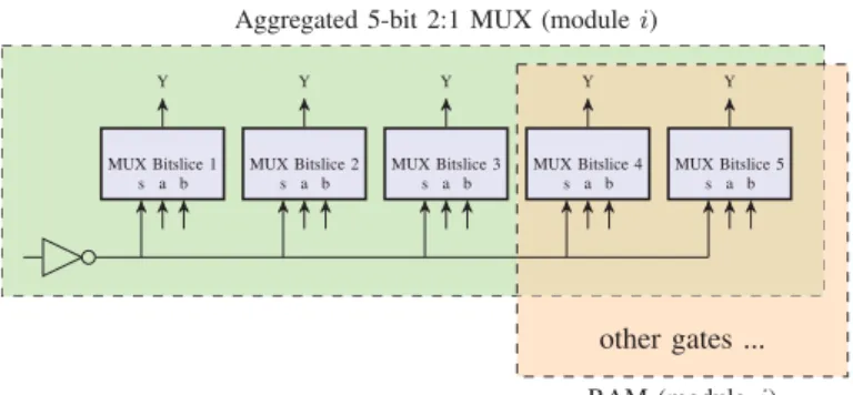
Aggregated 5-bit 2:1 MUX (modulei)
other gates ... RAM (modulej) MUX Bitslice 1 s a b Y MUX Bitslice 2 s a b Y MUX Bitslice 3 s a b Y MUX Bitslice 4 s a b Y MUX Bitslice 5 s a b Y
Fig. 8. Illustration of need for the “sliceable” formulation.
To motivate the need for the “sliceable” ILP formulation consider the example shown in Figure 8. One box shows a 5-bit 2:1 MUX aggregated using the common select signal. This box partially overlaps with a RAM module because two of the bitslices in the 2:1 MUX are also included in the RAM module. Overlaps such as this occur because the bitslice aggregation algorithms are “greedy” in the sense that these
inferred modules are created with the maximum number of bitslices matching the common select signal.
The basic formulation uses a single binary variable to either select or discard an inferred module. Therefore, the formula-tion will result in either the 2:1 MUX or the RAM being included in the final output but not both. This is suboptimal because there is a third option. The 2:1 MUX can be “sliced” to include the 3 bitslices that don’t overlap with the RAM and then the entire RAM can be included. In this section we develop an ILP formulation that allows modules to be “sliced” in this manner.
4.2.1 ILP Variables
Inferred modules are grouped into two categories. Modules like muxes and decoders which can be split up into indepen-dent bitslices are considered “sliceable”. If such a module has
nslices, it is modelled in the ILP withn+ 1binary variables:
xi0, xi1, . . . , xin. Variablexij wherej≥1represents whether slice j of module i is selected for output. Variable xi0 is a special variable introduced for technical reasons. It represents where modulei itself (i.e., any slice in modulei) is selected for output. In the example shown in Figure 8, suppose the 5-bit multiplexer is module i, then MUX bitslices 1, 2, 3, 4 and 5 will be represented by variables xi1, xi2, xi3, xi4 and
xi5 respectively.
Modules which are not “sliceable”, for example: counters and RAMs, are represented as before with a single binary variable xi which determines whether the entire module is selected for output or discarded.
4.2.2 Constraints Describing Overlaps
The formulation in§4.1.2 expressed the fact that if a gate is covered by l different modules, no more than one of these modules could be selected for output. Here, we would like to express the same but at the finer granularity of slices rather than modules. For this it is necessary to assign the elements included in a module to its component slices.
Define the following function V ar(gk, i) that maps an element gk contained in module i to the ILP variable that represents the slice that gk is contained in.
V ar(gk, i) = ⎧ ⎪ ⎪ ⎪ ⎨ ⎪ ⎪ ⎪ ⎩ xi if modulei is unsliceable xij ifgk is contained only in slice j of modulei xi0 otherwise
The intuition here is that for a sliceable module, elements which are contained in exactly one slice are mapped to that slice. Elements which are contained in more than one slice, are mapped to the variable xi0 which is the special variable that represents the entire module. Returning to the example in Figure 8, the gates which are inside the boxes labelled “MUX bitslicej” will be mapped to variablexij. The inverter however, is “part of” all bitslices, so it is mapped toxi0.
As before, suppose element gk is covered by inferred modulesk1, k2, . . . , kl. We add the following constraint.
V ar(gk, k1) +V ar(gk, k2) +· · ·+V ar(gk, kl)≤1
Consider a gate that is contained within the box labelled “MUX Bitslice 4” in Figure 8. The specific constraint intro-duced by a gate inside “MUX Bitslice 4” will bexi4+xj≤1. This tells the solver that either bitslice 4 or the RAM can be selected for output but not both. Unlike in the basic formulation, we are not restricting the selection of the other bitslices in the MUX.
4.2.3 Slice-Related Constraints
For each sliceable module, we would like to specify that if any individual slice is selected, gates that are common to more than one slice are also selected. This leads to constraints of the following form.
forall1≤j≤n: xi0−xij ≥0
In the notation above, moduleihasnslices and is modelled in the ILP using the variablesxi0, xi1, . . . , xin.
We would also like to specify that each module contains a minimum number of slices to avoid creating very small modules. This is done using a constraint of the form:
n j=1
xij − M inSlices·xi0 ≥0
n is the number of slices in module i.16 All results are
shown in this paper are with M inSlices= 2.
4.2.4 Objective Function
The objective function to maximize coverage is similar to that presented in §4.1.3 with the difference that we have to count “sizes” on a per-slice basis. Define the size function as follows.
Size(x) =gk | V ar(gk, i) =xfor some i
Clearly, Size(x) counts the number of elements covered by the variable x. Given Size(x) the objective function can be derived in a straightforward manner by weighting each variable with its corresponding size.
maximize
variablex
x·Size(x)
Returning to the example in Figure 8, the solver can maximize coverage by setting xi0, xi1, xi2, xi3 and xj to 1 and xi4 and xi5 to zero. This satisfies all the constraints we have described and selects bitslices 1, 2 and 3 of the MUX and the entire RAM.
16. Note adding the constraintNj=1xij ≥M inSlicesis incorrect. This requires every module to haveM inSlicesslices selected. What we want is:
if a module is selected, it must have at leastM inSlicesslices in it.
4.2.5 Alternative Formulation
The formulation that minimizes the number of inferred mod-ules while meeting the coverage target Ct again requires the addition of the following constraint.
variablex
x·Size(x)≥Ct
The following function returns the representative variable for a modulei. The representative variable determines whether a module is selected for output.
rep(i) =
xi if module iis not sliceable
xi0 if module iis sliceable
In the example shown in Figure 8, the representative vari-ables for the 5-bit multiplexer and RAM are xi0 and xj
respectively.
Assuming the total number of modules isM and that they are numbered from1toM, the objective function is now given by the following equation.
minimize M i=1 rep(i)
5
EXPERIMENTAL
RESULTS
We now present a detailed evaluation of our algorithms. 5.1 Methodology
We developed an inference tool using the C++ and Python programming languages that implement the algorithms de-scribed in this paper. The tool takes as input a synthesized verilog netlist, analyzes it and outputs an abstracted netlist with the inferred components. The tool uses the CU Decision Diagram (CUDD) Package version 2.4.2 for the BDD-based analyses [23], and MiniSat version 2.2 for satisfiability check-ing [6]. DepQBF [16] was used as the QBF solver and IBM CPLEX version 12.5 was the ILP-solver.
Experiments were performed on an IntelR XeonR E31230
CPU clocked at 3.20GHz with 32 GB of RAM. One set of results are shown for eight netlists. Details of these netlists are shown in Table 2. All the designs were synthesized using an IBM/ARM cell library for a 45nm SOI process. This paper also shows inference results on a large highly-optimized SoC design consisting of more than 375,000 combinational elements. A case study describing our analysis of this test article is given in Section 5.3. Finally, we describe a case study where we inject hardware trojans into two of the test articles from Table 2 and discuss how our algorithms would aid an analyst detect these trojans.
5.2 Summary of Results
Table 3 shows the modules identified and overall coverage obtained using our inference algorithms. Coverage is measured as a percentage of gates in the design which are covered by inferred modules. The table also shows information about the
TABLE 3 Coverage Results.
Design Information Combinational Sequential Coverage and components components execution time Design gate latch a/s dec dm eq gf mux lt ram sr cnt reg cov tim mem
router 896 182 0 44 10 0 46 281 0 0 0 4 8 65% 9s 0.6 0 10 0 0 28 48 0 0 0 4 8 64% 9s 0.7 eVoter 1360 108 0 41 8 8 205 7 72 0 0 0 1 53% 10s 0.6 0 11 1 0 44 5 16 0 0 0 1 45% 10s 0.7 Open8 1807 237 23 278 61 1 115 141 35 2 1 2 18 70% 31s 1.3 5 16 0 1 30 52 5 1 1 0 7 62% 32s 1.4 cpu8080 2258 243 6 402 58 0 181 173 129 0 0 0 8 64% 25s 1.2 6 15 1 0 73 75 6 0 0 0 5 61% 25s 1.2 ae18 3466 1094 27 602 118 0 164 216 99 1 3 2 57 69% 17s 1.0 7 21 2 0 50 71 5 0 2 1 12 65% 21s 1.1 MIPS16 6986 4380 2 1290 102 4 111 346 581 3 1 27 276 94% 19s 1.1 2 4 0 4 18 14 3 2 1 0 1 93% 36s 1.2 oc8051 8164 2748 20 5447 494 5 428 835 1842 8 4 5 304 79% 98s 4.0 5 48 3 4 109 141 11 4 3 5 17 76% 136s 4.3 RISC FPU 14291 3097 130 843 198 24 526 2887 1272 2 7 51 123 78% 185s 3.8 37 59 4 13 158 140 36 1 7 2 40 73% 196s 4.0
Legend for table header:gate: number of gates; latch: number of latches a/s: adders/subtractors; dec: decoders; dm: demultiplexers; eq: equality comparators; gf: gating functions (and2/or2 etc. of a word with a common signal); mux:multiplexors; lt: parity tree, zero-detect and one-detect; ram:RAMs/register files; sr: shift registers; cnt: counters; reg: registers; cov: coverage in percentage of gates covered; tim: execution time in seconds. mem: maximum resident set size in GB (proxy for memory consumption).
The white rows show results before overlap resolution while the shaded rows are inferred modules obtained after overlap resolution.
netlists being analyzed, the number of inferred modules of various types and the execution time of the tool.
For each test article, we show two rows. The white row shows the number of modules obtained before overlap res-olution. This means that for the results shown in the white rows, each gate/flip-flop/latch in the test article may be placed into multiple different inferred modules. These results are directly comparable to the results presented in [26]. The shaded rows show the results after overlap resolution (§4) has been performed. In this case, each gate/latch/flip-flop is placed in atmost one inferred module. The process of overlap resolution necessarily involves a small loss in coverage but we see from the results shown that the loss is quite small.
For the three biggest netlists, coverage is above 70% and reaches up to 93% for the 16-bit MIPS CPU. These netlists all have a large number of replicated bitslices in the datapath which are captured well by the bitslice identification and aggregation algorithms. In contrast, the smaller netlists have a significant fraction of gates devoted to irregular control logic, which is hard to identify in a fully automated solution.
Both the execution time and memory requirements posed by the analysis tool are very reasonable. The maximum execution time among this set of designs is a little more than three minutes and the maximum resident set size is 4.1GB. The most computationally-expensive algorithm in our toolbox is the counter analysis.
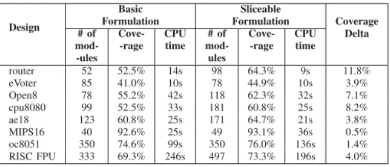
5.2.1 Sliceable vs. Basic ILP Formulation
Table 4 compares the basic ILP formulation (§4.1) with the sliceable ILP formulation (§4.2). Recall that the basic formulation can only select or discard an entire module, while
the sliceable formulation can select or discard a subset of the bitslices in a multibit module. We expect that the sliceable formulation will always have the same or better coverage than the basic formulation. However, the trade-off here is again that the sliceable formulation will somtimes tend to choose a few smaller modules over one big module. Results in Table 4 are in keeping with these expectations.
TABLE 4
Comparing the Sliceable and Basic Formulations.
Design
Basic Sliceable
Formulation Formulation Coverage # of Cove- CPU # of Cove- CPU Delta mod- -rage time mod- -rage time
-ules ules router 52 52.5% 14s 98 64.3% 9s 11.8% eVoter 85 41.0% 10s 78 44.9% 10s 3.9% Open8 78 55.2% 42s 118 62.3% 32s 7.1% cpu8080 99 52.5% 33s 181 60.8% 25s 8.2% ae18 123 60.8% 25s 171 64.7% 21s 3.8% MIPS16 40 92.6% 25s 49 93.1% 36s 0.5% oc8051 350 74.6% 99s 350 76.0% 136s 1.4% RISC FPU 333 69.3% 246s 497 73.3% 196s 4.0%
5.3 Case Study 1: Analysis of BigSoC Test Article We present a case study of algorithmic reverse engineering of large, realistic SoC. This SoC consists of 375090 combi-national elements, 34318 latches and 62 and 94 inputs and outputs respectively. We describe the three part strategy we used to analyze this design in the rest of this subsection.17 Besides the gate-level netlist, we were also given a datasheet