First-principles study on oxidation of Ge and
its interface electronic structures
著者
Ono Tomoya, Saito Shoichiro, Iwase Shigeru
journal or
publication title
Japanese journal of applied physics
volume
55
number
8S2
page range
08PA01
year
2016-08
権利
(C) 2016 The Japan Society of Applied Physics
URL
http://hdl.handle.net/2241/00144538
First-principles study on oxidation of Ge and its interface electronic
structures
Tomoya Ono1,2∗, Shoichiro Saito3, and Shigeru Iwase4
1Center for Computational Sciences, University of Tsukuba, Tsukuba, Ibaraki 305-8577, Japan 2JST-PRESTO, Kawaguchi, Saitama 332-0012, Japan
3Nitto Denko Corporation, Ibaraki, Osaka 567-8680, Japan
4Graduate School of Engineering, Osaka University, Suita, Osaka 565-0871, Japan
We review a series of first-principles studies on the defect generation mechanism and electronic structures of the Ge/GeO2interface. Several experimental and theoretical studies proved that Si atoms at the Si/SiO2
interface are emitted to release interface stress. In contrast, total-energy calculation reveals that Ge atoms at the Ge/GeO2interface are hardly emitted, resulting in the low trap density. Even if defects are generated,
those at the Ge/GeO2 interface are found to behave differently from those at the Si/SiO2 interface. The
states attributed to the dangling bonds at the Ge/GeO2interface lie below the valence-band maximum of
Ge, while those at the Si/SiO2interface generate the defect state within the band gap of Si. First-principles
electron-transport calculation elucidates that this characteristic behavior of the defect states is relevant to the difference in the leakage current through the Si/SiO2and Ge/GeO2interfaces.
1. Introduction
The impressive increase in the performance of microelectronic devices has been achieved by the continuous decrease in the length scale, which is approaching its technological and physical limits. However, it is becoming increasingly difficult to enhance the performance of complementary metal-oxide-semiconductor (MOS) devices through scaling based on con-ventional Si-based techniques. A considerable number of studies have been conducted to find alternative materials to further increase the performance of MOS field-effect transistors. Ge is considered as one of the best channel materials owing to its high intrinsic carrier mobility. Although the first bipolar transistor developed by Bardeen, Brattain, and Shockley consists of Ge/GeO2, interest on Ge-based devices has decreased with the advancement of Si/SiO2-based transistors. This is because Ge/GeO2 interfaces have generally been considered to include more defects than Si/SiO2 interfaces, wherein the interface trap density typically lies in the range of the latter half of 1011−1012cm−2eV−1.1)It is a general consensus that the formation
of MOS interfaces with superior properties is the key issue to be resolved, and the interface properties are closely relevant to interface trap density. Thus, the understanding and control of the defects at the Ge/GeO2interface are important to enhance the performance of Ge-based devices because the Ge/GeO2interface exists even in Ge/high-koxide interfaces.
In the last decade, a considerable number of studies have been made on the fabrication of high-quality Ge/GeO2 interfaces, and the low interface trap density in the Ge/GeO2interface can be achieved using a cap layer,2)high-pressure thermal oxidation,3, 4)or ozone oxidation.5) In 2008, Matsubara et al.6) reported that the minimum interface trap density of lower than 1011cm−2eV−1, which is lower than that in typical Si/SiO
2 interfaces without any hydrogen forming gas annealings, can be obtained for the Ge/GeO2 interface fabricated by the dry oxidation without any hydrogen passivation treatment. In the following year, Hosoi et al.7) fabricated a high-quality Ge/GeO2interface by the conventional thermal treatment of Ge sub-strates. In addition, Lee et al.4) also reported that the electrical properties of metal/GeO2/Ge capacitors fabricated by the high-pressure oxidation of Ge are improved and the interface state density is reduced to 2×1011cm−2eV−1 near the middle of the valence-band maximum (VBM) and conduction-band minimum (CBM) of Ge even when post-deposition annealing is carried out. On the theoretical side, the structural and electronic properties of the Ge/GeO2 in-terface have been investigated by first-principles calculations based on the density functional theory8, 9) and/or other methods avoiding the band gap problem in the local density approxi-mation in the density functional theory. Houssa et al.10) simulated the density of Ge-DBs at the Ge/GeO2interface as a function of oxidation temperature, by combining the viscoelastic data of GeO2 and the modified Maxwell’s model, and claimed that the density of Ge-DBs is less than that of Si-DBs. The present authors found that hardly any defects are generated at the Ge/GeO2interface compared with the number generated at the Si/SiO2 interface from the formation energy of defects at the Ge/GeO2 interface.11) In addition, Weber et al.12) and Broqvistet al.13)investigated the electronic structure of the defects in Ge bulk, which are ex-pected to affect the interface properties, by the G0W0 approximation14) and the hybrid func-tional method,15) respectively. They reported the different behaviors of the dangling bonds (DBs) at the Ge/GeO2interface from those at the Si/SiO2interface.
In this article, we review the first-principles studies on the oxidation of Ge and its interface electronic structures together with relevant experimental results. In Sect. 2, studies on the interface atomic structures as well as defects are introduced in comparison with the case of Si. The simulations for the interface electronic structure and gate leakage current are reported in Sect. 3. Finally, our summary is given in Sect. 4.
(a)
(b)
(c)
y
x
z
[110]
[110]
[001]
_
(d)
(e)
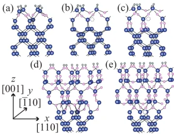
Fig. 1. (Color online) Atomic configurations of models. (a) Surface model where no Ge atom is emitted
from the structure that includes three O atoms, (b) surface model where one Ge atom per unit cell is emitted from the structure including three O atoms, and (c) surface model where one Ge atom per unit cell is emitted from the structure including six O atoms. Interface models in which three additional O atoms are inserted into the Ge/GeO2interface (d) before emission and (e) after emission. The gray (light small), blue (dark large), and pink (light middle) balls are H, Ge, and O atoms, respectively. The hatched circles are the Ge atom being emitted and the broken circles indicate the position where the Ge atom is emitted.
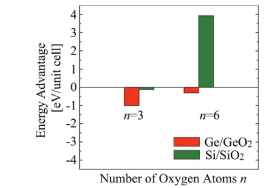
Fig. 2. (Color online) Energy advantage of Ge- and Si-emitting structures compared with nonemitting
structures, as a function of the number of O atoms per unit celln. Reprinted with modification with permission from Ref. 11. Copyright 2009 AIP Publishing LLC.
2. Interface atomic structure 2.1 Atom emission from the interface
The structural and electronic properties of Ge/GeO2interfaces have been investigated by sev-eral groups.10, 11, 16–24)Although the residual order at Si/SiO2interfaces has been observed by transmission electron microscopy,25) that at Ge/GeO2 interfaces has not. Some studies18, 23)
Fig. 3. (Color online) Energy advantage of Ge- and Si-emitting structures compared with nonemitting structures in the case of interface.
use the models in which amorphous GeO2 is attached to the Ge substrate to investigate electronic structures; however, it is not easy to derive definite conclusions using the models employing amorphous GeO2 because the model size treated by first-principles calculations is small to eliminate the effect of artificial periodic boundary conditions. Therefore, many studies10, 11, 16, 17, 19–22, 24) adopt the interface atomic structures based on their Si/SiO
2 counter-parts,26)where crystalline GeO
2 is attached to a Ge substrate.
Houssa et al.10) simulated the density of Ge-DBs at the Ge/GeO
2 interface as a func-tion of oxidafunc-tion temperature, by combining the viscoelastic data of GeO2 and the modi-fied Maxwell’s model, and claimed that the density of Ge-DBs is less than that of Si-DBs. Their results are in good agreement with the experimental results.4, 6, 7) However, the forma-tion mechanism of defects in the Ge/GeO2 interface region during the oxidation is not well known.
The oxidation of the Si/SiO2interface was simulated by Kageshima and Shiraishi27, 28) us-ing first-principles calculations and they found that a quartz phase can be obtained if Si atoms are kicked out from the interface during oxidation. Later, using the larger model, Yamasaki et al.29) also demonstrated that the Si-atom emission from the Si/SiO
2 interface occurs and
Pb-type defects are formed during oxidation. Moreover, the experiment using high-resolution Rutherford backscattering spectroscopy assured the Si-atom emission.30) In the case of the oxidation of Ge, it is reported that the volatilization of GeO from Ge atoms driven by the reaction at the Ge/GeO2interface is the origin of the deterioration of the interface.2) In addi-tion, the interface quality can be improved by suppressing the out-diffusion of GeO to the air
using a cap layer on the top of GeO2. Therefore, the Ge-atom emission from the interface is strongly relevant to realize the low trap density in the Ge/GeO2interface.
The probability of the Ge-atom emission from the Ge/GeO2 interface is compared with that from the Si/SiO2 interface in terms of the total-energy calculation.11) The calculations are performed on the basis of the density functional theory using the RSPACE code.31–34) Figure 1 shows examples of the Ge(100) surface models. O atoms are sequentially inserted between Ge-Ge bonds from the surface, assuming atomic layer-by-layer oxide growth, and finally six O atoms are introduced into the unit cell. In the case of the oxidation of Si, the first-principles calculations revealed that the Si atom in the second layer will be emitted to release the interface stress.27, 28) The example for the case ofn = 3 is illustrated in Figs. 1(a) and 1(b), where nis the number of inserted O atoms. The hatched atom is emitted and goes elsewhere. The emission generates DBs at the interface when nis smaller than 5. When six O atoms are introduced, these DBs are perfectly terminated by the formation of a Si-O-Si or Ge-O-Ge bond, as shown in Fig. 1(c). By comparing the total-energy difference between the atomic configurations before and after the emission, the energy advantage can be defined as Enon(n)−[Eemi(n)+µ], whereEnon(n) andEemi(n) are the total energies of the nonemitted and emitted structures withnO atoms inserted, respectively, andµis the chemical potential of Ge or Si in the bulk phase. The energy advantages of Ge and Si as a function of the number of inserted O atoms are shown in Fig. 2. When the number of inserted O atoms is 1, the energy advantage of Si for the atom emission is smaller than that of Ge because the formation energy of a monovacancy is significantly larger in Si (∼3.3 eV)35)than in Ge (∼1.9 eV).36)However, the energy advantage of Si-atom emission increases more rapidly as the number of inserted O atoms increases and becomes greater than that of Ge. The Si-atom emission from the surface model is preferred whennis larger than 3, while the Ge atom is not emitted until the number of inserted O atoms becomes 6. As a further oxidation model, Figs. 1(d) and 1(e) show examples of the interface models. The energy advantages for the atom emission from the interface are shown in Fig. 3, indicating the lower energy advantage of Ge than that of Si. These results indicate that the Ge atom preferentially remains in the substrate during the oxidation. In addition, the emitted atoms might be the source of self-interstitials, resulting in the creation of these interstitials at the interface or in the substrate. These interstitials cause the degradation of the MOS device, such as leakage current and scattering centers of inversion carriers. Because the formation energy of the Si self-interstitials (∼3.5 eV) is almost equal to that of Ge self-interstitials,37, 38)the high energy advantage of the Si-atom emission causes the generation of the self-interstitials at the interface. Moreover, the trap density of the Ge/GeO2
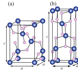
(a) (b) (c) a a a a a c c a c 60°
Fig. 4. (Color online) Unit cells of (a) quartz, (b) cristobalite, and (c) rutile. Pink (light) and blue (dark)
balls are O and Ge (Si) atoms, respectively.
Table I. Calculated and experimental lattice constants (in Å).
a c q-GeO2 4.897 5.636 c-GeO2 4.818 7.128 r-GeO2 4.418 2.886 q-SiO2 4.850 5.348 c-SiO2 4.925 6.828 r-SiO2 4.147 2.662
interface becomes lower than that of the Si/SiO2 interface, since the events creating volatile GeOs, the DBs, and self-interstitials at the interface rarely occur.
2.2 Atomic structure of oxides under interface stress
It is of interest to explore the reason why the emission probability from the Ge/GeO2interface is smaller than that from the Si/SiO2interface. One of the intuitive possibilities is the diff er-ence in the lattice-constant mismatch between the substrate and the oxide. When O atoms are simply inserted between Ge-Ge bonding networks, cristobalite GeO2is formed. However, the bonding networks attain a lattice-constant mismatch of 21%, which is almost the same as that between Si and SiO2.
o 3
o 3
(a)
(b)
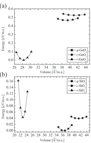
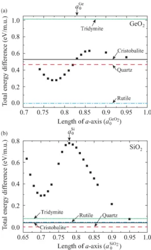
Fig. 5. Total energy per molecular unit (m.u.) as a function of volume for all polymorphs of (a) GeO2and
(b) SiO2. The zeros of energies are the rutile phase for GeO2and the quartz phase for SiO2. Reprinted from Ref. 40.
Table II. Bond lengthsli(in Å), bond anglesθj, and tilt anglesδ(in deg) of GeO2and SiO2polymorphs.θ1,
θ2,θ3, andθ4are the O-x-O angles, where x represents a Ge or Si atom.liandθjare assigned according to
magnitude. l1 l2 θ1 θ2 θ3 θ4 δ q-GeO2 1.763 1.755 114.13 110.69 107.28 105.39 29.66 c-GeO2 1.760 1.760 120.69 111.39 109.95 101.72 35.64 r-GeO2 1.918 1.887 80.25 q-SiO2 1.608 1.603 110.58 109.37 109.23 108.55 17.85 c-SiO2 1.604 1.603 111.46 110.02 109.01 108.15 25.41 r-SiO2 1.786 1.751 81.02
Si atom shows fourfold coordination, while rutile GeO2, in which a Ge atom shows sixfold coordination, has the lowest energy among GeO2 polymorphs.39) Detailed analyses of the structural variations of three GeO2and SiO2polymorphs,α-quartz,α-cristobalite, and rutile, under compression and expansion pressure are conducted.40) Here and hereafter, we
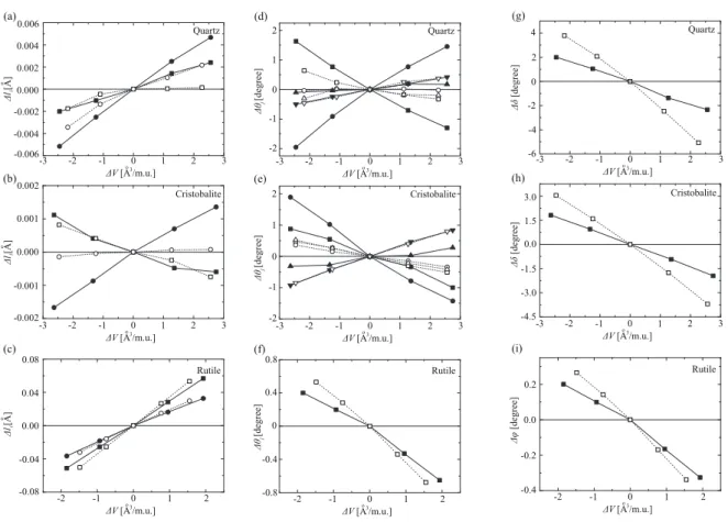
abbre-Δl [A ] o i ΔV [A /m.u.] -3 -2 -1 0 1 2 3 3 o 0.006 0.004 0.002 0.000 -0.002 -0.004 -0.006 Quartz 0.001 0.002 0.000 -0.002 -0.001 ΔV [A /m.u.] -3 -2 -1 0 1 2 3 3 o Cristobalite Δl [A ] o i Rutile ΔV [A /m.u.] -2 -1 0 1 2 3 o 0.08 0.04 0.00 -0.04 -0.08 Δl [A ] o i (a) (b) (c) ΔV [A /m.u.] -3 -2 -1 0 1 2 3 3 o Δθ [de gre e] j -2 -1 0 1 2 Δθ [de gre e] j -2 -1 0 1 2 ΔV [A /m.u.] -3 -2 -1 0 1 2 3 3 o ΔV [A /m.u.] -2 -1 0 1 2 3 o Δθ [de gre e] j -0.8 -0.4 0 0.4 0.8 (d) (e) (f) Quartz Cristobalite Rutile Δδ [de gre e] ΔV [A /m.u.] -3 -2 -1 0 1 2 3 3 o 4 2 0 -2 -4 -6 ΔV [A /m.u.] -3 -2 -1 0 1 2 3 3 o 3.0 1.5 0.0 -1.5 -3.0 -4.5 Δδ [de gre e] 0.2 0.0 -0.2 -0.4 ΔV [A /m.u.] -2 -1 0 1 2 3 o Δφ [de gre e] (g) (h) (i) Quartz Cristobalite Rutile
Fig. 6. Variations of x-O bond lengths∆liin (a) quartz, (b) cristobalite, and (c) rutile phases from their
equilibrium points.∆l1and∆l2correspond to squares and circles, respectively. Variations of O-x-O bond angles∆θjin (d) quartz, (e) cristobalite, and (f) rutile phases.∆θ1,∆θ2,∆θ3, and∆θ4correspond to squares, circles, upper triangles, and lower triangles, respectively. Variations of x-O-x bond angles∆δin (g) quartz and (h) cristobalite phases. Variations of x-O-x bond angles∆φin (i) rutile phase. x represents a Ge or Si atom. Black (white) symbols are the results of GeO2(SiO2) and lines are only eye guides. Reprinted with modification from Ref. 40.
viateα-quartz GeO2, α-cristobalite GeO2, and rutile GeO2 as q-GeO2, c-GeO2, and r-GeO2, respectively. The same abbreviations are applied for SiO2polymorphs. Ge or Si atoms in the quartz and cristobalite phases are surrounded by four O atoms while those in the rutile phase is surrounded by six O atoms with distorted octahedral coordination, as shown in Fig. 4. The total energies per molecular unit as a function of volume for the three phases are shown in Fig. 5, in which the zeros of energy are the rutile phase for GeO2 and the quartz phase for SiO2. In the periodic table, Ge is between Si and Sn, which is also a group IV element and is a metal. In addition, under ambient conditions, SnO2crystallizes in the rutile phase,41)where d bands of metal atoms lie below the Fermi level.42) Since 3d orbitals of Ge are occupied, GeO2 forms the sixfold rutile phase more preferentially than SiO2.
and SiO2 are listed in Tables I and II. From the viewpoint of atomic geometry, there are two distinct Ge-O (Si-O) bond lengths in the GeO4(SiO4) tetrahedron. In addition,θj are the O-Ge-O (O-Si-O) bond angle,43, 44) and the tilt angle is related to the Ge-O-Ge (Si-O-Si) bond angle. The deviations of the O-Ge-O bond angles from the ideal tetrahedral angle (109.5◦) are found to be larger than those for O-Si-O, which results in a distorted GeO4 tetrahedron.
The lattice-constant mismatch between Ge (Si) and its oxide induces the compressive in-plane stress at the Ge/GeO2 (Si/SiO2) interface. Since it is found by X-ray photoelectron spectroscopy that the thermal oxidation mainly generates the fourfold structure,45, 46)the bond structures of crystalline quartz and cristobalite phases are examined under the assumption that the oxidation mechanism of Ge is the same as that of Si. The variations of the Ge-O (Si-O) bond lengths, the O-Ge-O (O-Si-O) bond angles, and the tilt angles with respect to the volume are shown in Fig. 6. The variation of the tilt angles in the rutile phase is expressed as ∆φ because there are no tetrahedrons in the rutile phase. It is found that the variations of the bond lengths are quite small and less than ∼0.1% even when the lattice constants are increased by 1%. This result indicates that the bond angles are important properties in the compression or expansion of the fourfold structure. When GeO2is compared with SiO2, the variations of the bond anglesθjin GeO2are larger than those in SiO2[Figs. 6(d) and 6(e)], while the tilt angles δin SiO2vary more significantly than those in GeO2[Figs. 6(g) and 6(h)]. When the stiffness of the tilt angle around the O atom is assumed to be comparable between SiO2and GeO2, this result implies that the O-Si-O bonds are more rigid than the O-Ge-O bonds. The experimental study also reported that the O-Ge-O bond angles markedly change in q-GeO2, while the tilt angle in q-SiO2 varies significantly as the pressure increases.47) These structural properties under compression or expansion agree well with the experimental result. Such chemical trend of Ge in the periodic table is also attributed to the distorted GeO4tetrahedron and the variation of the O-Ge-O bond angles from the ideal tetrahedral angle. These structural properties of the O-Ge-O bonds contribute to the reduction in the interface stress during oxidation compared with its Si counterpart, resulting in the low emission probability from the Ge/GeO2interface. 2.3 Atomic structure of oxides above the substrate
Although the stress at the Ge/GeO2 interface is expected to be small, it has to be released somewhere from the macroscopic viewpoint. Then, the atomic structures of GeO2and SiO2 bulks in the cristobalite phases (c-GeO2 and c-SiO2) under pressure along thea-axis are in-vestigated because these structures correspond to the directions parallel to the interface when the oxides are piled on the (001) surface.20)Figure 7(a) shows the initial atomic configuration,
in which the c-GeO2(c-SiO2) structure illustrated is tetragonal. The length of thea-axis from the equilibrium lattice constants, aGeO2
0 (=4.818 Å) anda S iO2
0 (=4.925 Å) for GeO2 and SiO2, respectively, is compressed. The total energies of c-GeO2 and c-SiO2 per molecular unit as a function of volume are shown in Figs. 8(a) and 8(b), respectively. The zeros of energy are the rutile phase for GeO2 and the quartz phase for SiO2. For comparison, the energy minima of other phases (quartz, cristobalite, tridymite, and rutile) without any constraints are also plotted. The c-GeO2 shows a local minimum at about 0.78aGeO20 . The c-GeO2under a certain pressure transforms into a sixfold structure as shown in Fig. 7(b), which is distinct from the rutile phase, by rotating O atoms around the Ge atoms. The energy minimum of sixfold GeO2 is lower than that of fourfold GeO2 since the zero-temperature phase of GeO2 has a sixfold rutile phase as discussed in Sect. 2.2. The arrow on the upper horizontal axis corresponds to the lateral length of the Ge(001)-(1× 1) surface. Note that GeO2 forms a sixfold structure when the length of the a-axis is equal to that of the (1 ×1) surface, while the c-SiO2 still maintains a fourfold structure.
Since the lattice-constant mismatch between the sixfold GeO2 and Ge(001) surfaces is small (∼5%), the interface stress may be released by partially forming r-GeO2 at the inter-face. Therefore, it is of interest to compare the energetic stability of the sixfold GeO2/Ge(001) interface with the fourfold one. Computational models are shown in Fig. 9. To set up the inter-face models, O atoms are sequentially inserted between Ge-Ge (Si-Si) bonds from the (001) surface as we assumed the layer-by-layer oxide growth in Sect. 2.1. The sixfold structure is formed by rotating the four O atoms around one Ge atom in a Ge(001)-(1×1) surface unit. The sixfold GeO2/Ge interface is more stable by 1.92 eV per Ge(001)-(
√
2× √2) than the fourfold one, while the fourfold c-SiO2/Si interface model is preferable by 1.02 eV compared with the sixfold one. The interface stress between GeO2 and Ge is released by the phase transition into the dense sixfold structure. These results indicate that the sixfold structure contributes to the release of interface stress due to the lattice-constant mismatch between the c-GeO2 and Ge(001) surfaces as well as the small possibility of the Ge-atom emission from the interface during oxidation.
Since the lateral length of the Ge(001)-(1× 1) surface is longer than that of the sixfold GeO2 surface but shorter than that of the fourfold c-GeO2 surface in Fig. 8(a), c-GeO2 on the Ge(001) surface might be composed of a mixed fourfold and sixfold structure. Figure 10 shows the computational model, in which the supercell is the doubling of the Ge(001)-(√2×
√
2) surface unit in two directions. One and five neighboring (1 × 1) Ge surface units are replaced by the sixfold structure so that 12.5 and 62.5%, respectively, of the Ge(001)-(1 ×
(a)
(b)
a a c a a cFig. 7. (Color online) Unit cells of (a) fourfold and (b) sixfold c-GeO2. The solid cube represents the
unit-cell volume, and the blue (dark) and pink (light) balls are Ge and O atoms, respectively.
1) units are composed of the sixfold structure. The mixed interface with the 12.5% sixfold structure is even more unstable than the fully fourfold GeO2/Ge interface by 0.92 eV, although that with the 62.5% sixfold structure is more stable by 0.49 eV. The domain boundary causes the instabilities of the mixed structures; the c-axis of the fourfold-structure region is more than 5% longer than that of the sixfold one. Therefore, the sixfold-structure region can exist as a large domain at the GeO2/Ge interface so that the domain boundary is minimized. 3. Electronic structure of the defects at the interface and its contribution to
leakage current
3.1 Dangling bond states at the interface
Since several experimental and theoretical studies have proved that the interface trap density in the Ge/GeO2 interface is smaller than that at the Si/SiO2 interface without any annealing, the future development of passivation technologies to deactivate interface defects by intro-ducing terminators will make it possible to decrease the interface trap density in the Ge/GeO2 interface further. However, experimental and theoretical studies revealed that the defects are not passivated by H2 annealing in contrast to Si technology.19, 48, 49) Thus, understanding the morphology and electronic structure of interface defects is one of the key issues to develop passivation technologies.
It is well known that the DB states at the Si/SiO2 interface can be detected by electron spin-resonance (ESR) because the defect states lie between the VBM and the CBM of Si.50) Afanas’evet al.48)found that interfacial DB defects at the Ge/GeO2interface play a different
Fig. 8. (Color online) Total energy per molecular unit (m.u.) as a function of lengths ofa-axis for (a) c-GeO2 and (b) c-SiO2. The horizontal axes correspond to the lateral lengths of Ge and Si(001)-(1×1) surfaces inaGeO2
0 anda
S iO2
0 . Total energies of quartz [red (black) dashed line], cristobalite (black solid line), tridymite [green (black) dotted line], and rutile [blue (black) long dashed short dashed line] are also shown for comparison. The zeros of energies are rutile for GeO2and quartz for SiO2. Vertical arrows indicate lattice constants of Ge (aGe
0 ) and Si (a
S i
0 ) bulks, respectively. Reprinted with permission from Ref. 20. Copyright 2011 Amreican Physical Society.
role from those at the Si/SiO2interface using ESR; a measurable density of DBs of the semi-conductor surface atoms is not found at Ge/GeO2interfaces, and the defects characterized by an isotropic signal with g∼2.002−2.004 are observed instead. However, there remains a cer-tain amount of interface defects because the interface trap density shown in Ref. 48 was still higher than that of typical Si/SiO2interfaces after hydrogen annealing. This result implies the ESR inactivity of the Ge-DBs at Ge/GeO2interfaces.
From the viewpoint of the electronic structure of the DBs, the position of the DB states in Ge bulk is investigated by theG0W0approximation12)and the hybrid functional method.13) The former claimed that the DBs in Ge bulk have energy levels below the VBM of Ge and are
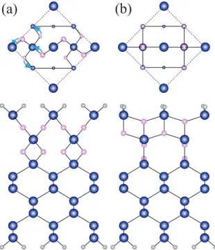
(a)
(b)
Fig. 9. (Color online) Top views and side views of (a) fourfold and (b) sixfold GeO2/Ge(001) interfaces.
The blue (dark large), pink (light middle), and grey (light small) balls are Ge, O, and H atoms, respectively. The dotted square in the top views represents a Ge(001)-(√2×√2) surface unit and the arrows indicate rotational directions to transform into sixfold structures.
(a)
(b)
Fig. 10. (Color online) Top views of mixed fourfold and sixfold structures. (a) 12.5 and (b) 62.5% of
Ge(001)-(1×1) surface units are composed of the sixfold structures. The blue (dark) and pink (light) balls are Ge and O atoms, respectively.
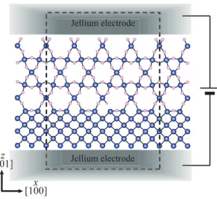
[001] [100] [001]] Jellium electrode Jellium electrode x z
Fig. 11. (Color online) Schematic image of computational model for interface. The rectangle enclosed by
broken lines represents the scattering region when the leakage current is calculated. Blue (dark large), pink (light middle), and gray (light small) balls represent Ge (Si), O, and H atoms, respectively.
therefore negatively charged. In contrast, the latter reported that the DBs in Ge bulk induce two very close defect levels lying just above the VBM within the certain range of the empirical mixing parameter of the hybrid functional method. Although these studies derive the opposite conclusions, they raised questions about the difference in the electronic structure between the Ge-DBs in Ge bulk and the Si-DBs in Si bulk, and the contribution of the interface stress caused by the lattice-constant mismatch between the semiconductor and the oxide to the position of the DB states. Here, we introduce first-principles study on the difference in the electronic structure between two interfaces21) using the RSPACE code. The interface atomic structure, consisting of an α-quartz crystalline oxide layer on a (001) substrate, is shown in Fig. 11. The DBs at the interface are generated by removing one O atom from the interface and terminating one DB by H atom.
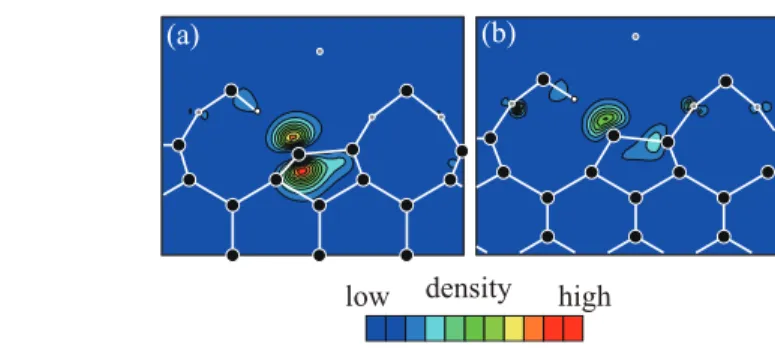
The lattice-constant mismatch between Ge (Si) and GeO2 (SiO2) induces the interface reconstruction, which is not taken into account in the Ge (Si) bulk model.12, 13) Thec-axis is slightly longer than the axis of the bulk (less than 1%) in both the Ge and Si cases, whereas the a-axis of the α-quartz oxide is 11% (9%) longer than the corresponding axis of the Ge (Si) bulk. Thus, the stress acting on the interface atoms is similar for both GeO2 and SiO2. Figure 12 shows the interface atomic structure after structural optimization. The interface Ge atom with the DB is raised up while the Si atom is pulled down so that theπelectron forms aPb-type defect in the Si substrate.
(a) (b)
high low density
Fig. 12. (Color online) Atomic structures of interfaces and contour plots of charge density distributions of
DB states. The planes shown are along the cross section in the (110) plane including DBs. (a) Si-DB state at
EFand (b) Ge-DB state atEF−0.3 eV. The lowest contours are 6.75×10⁻³e/Å3and the subsequent contour
lines represent values larger than 6.75×10⁻³e/Å3. The symbol meanings are the same as those in Fig. 11. Reprinted from Ref. 21.
investigation of the relationship between the atomic configuration and the electronic structure. Figure 13 is plotted by integrating the DOS along the plane parallel to the interface,ρ(z,E)= ∫
|ψ(⃗r,E)|2d⃗r||, where⃗r = (x,y,z),⃗r|| = (x,y), ψ is the wave function, and E is the energy of the states. Note that the energy band gap of Si and Ge substrates is underestimated owing to the usage of the local density approximation.51) The states accumulating at E
F −1.0 eV and indicated by the red downward arrows in Fig. 13(c) [Fig. 13(a)] are attributed to the Ge-(Si-) O bonds, whereEF is the Fermi level, since the charge density distributions accumulate between the Ge- (Si-) and O-atom layers. In the case of Si, when the DB is introduced in the Si/SiO2 interface, the DOS at EF −1.0 eV decreases and the state appears in the energy band gap, indicated by the white downward arrows in Fig. 13(b). On the other hand, the peak of the DOS at EF − 1.0 eV related to the Ge-O bonds becomes shallow, and the DOS at
EF −0.3 eV, denoted by the white downward arrows in Fig. 13(d), increases in the case of the Ge/GeO2 interface. In the periodic table, Ge exists between Si and Sn, the latter being metallic. The Ge-O bonds at the interface do not have a strongly preferential sp3-bonding direction.11)Thus, the bonding network of Ge/GeO
2is easily deformed from the sp3structure and exhibits more metallic properties than that of Si/SiO2. In addition, the band gap of the diamond structure of group IV elements is formed by the energy difference between sp3 bonding and antibonding states, and the energy gain due to the formation of covalent bonds in Ge is smaller than those in Si. These characteristics of Ge and the larger offset of the VBM than that of the CBM at the interface20, 26) contribute to keeping the DB states below the VBM of Ge. Moreover, Haneman52) reported that the sp3 DB on the Si surface is stabilized owing to the strong contribution of the s electron when the atom with a DB is raised up. The
Energy (eV)0 −2 2 (a) (b) Energy (eV)0 −2 2 Energy (eV)0 −2 2 Energy (eV)0 −2 2 (c) (d) Ge (w/o DBs) Si (w/o DBs) Si (w/ DBs) Ge (w/ DBs) z z z z high low density
Fig. 13. (Color online) Distributions of DOS integrated on a plane parallel to the interface as functions of
relative energy from the Fermi level. (a) Si/SiO2without DBs, (b) Si/SiO2with DBs, (c) Ge/GeO2without DBs, and (d) Ge/GeO2with DBs. The zeros of energies are chosen to be the Fermi level. Each contour represents twice or half the density of the adjacent contour lines, and the lowest contour is 1.45×10⁻⁴e/eV/Å. The solid and dashed lines represent the vertical positions of Si (Ge) and O atomic layers, respectively. The right arrows denote the positions of the Si and Ge atoms forming DBs. Reprinted from Ref. 21.
relationship between the position of the DB states and the atomic configuration in this study is consistent with the model proposed by Heneman. Therefore, the significant difference in the ESR signal from Ge-DBs48) is caused by the difference in the electronic structures and atomic configurations from Si-DBs.
Later, Houssaet al.49)claimed that the ESR signal observed at Ge/GeO2interfaces could be assigned to a DB at a Ge atom backbonded to two Ge atoms and one O atom, which does not contradict the results obtained by the above-mentioned electronic-structure calculation.
Chang et al.22) also investigated the Ge-DBs with different O backbonds at Ge/GeO
2 inter-faces and reported, on the basis of the hybrid functional method, that the state of thePb-type defect with the Ge atom backbonded to three Ge atoms lies above the VBM. However, the mixing parameter of the hybrid functional method, which significantly affects the position of the DB state,18) is large so that the state appears above the VBM, and thus the effect of the mixing parameter on the position of interface DB states is still controversial in the hybrid functional method.
3.2 Gate leakage property of the metal-oxide-semiconductor structure
In the case of the Si/SiO2interface, the Pb-type defect increases the leakage current.53)Since the state attributed to the Ge-DB does not lie inside the band gap of Ge, it is interest-ing to determine whether the leakage current is increased by the presence of the Ge-DBs at the interface. The recent evolution of the computational technique of the first-principles electron-transport calculation enables us to investigate the relationship between the interface defects and the leakage current.54, 55)Applicability to first-principles electron-transport calcu-lation31, 56, 57) is one of the advantages of the real-space finite-difference method31, 58, 59) over the other first-principles calculation methods, e.g., plane-wave expansion60) or linear com-bination of atomic orbitals.61, 62) The computational model for the transport calculation is illustrated in Fig. 11. The MOS interface is sandwiched between the metallic electrodes, and the conductance for the electrons coming from the lower electrodes to the upper one is calcu-lated, assuming that electrons accumulate at the interface by gate bias.55)Figure 14 shows the conductance spectra of the interface with and without the DBs. The conductance spectrum corresponds to the differentiation of the amount of leakage current with respect to the bias voltage. Although the Fermi level is determined by the work function of the electrodes, the overall feature of the local DOS at the interfaces does not change; the states of the Ge-DBs are under the VBM while those of the Si-DB lie between the VBM and the CBM. The tun-neling probability for the leakage current exponentially increases with respect to the energy difference between the incident electron and the conduction band, which is the barrier height. Because the band gap of GeO2is smaller than that of SiO2, the conductance of the Ge/GeO2 interface is larger than that of the Si/SiO2interface. When the DB is introduced to the Si/SiO2 interface, the sharp peak due to the contribution of the DB appears in the conductance spec-trum. On the other hand, the significant contribution of the Ge-DB states is not observed in the case of the Ge/GeO2interface. This is because the Ge-DB states spread energetically and are coupled with the states of the substrates, resulting in the shallow peak in the conductance
(a)
(b)
Fig. 14. (Color online) Conductance of the Si/SiO2and Ge/GeO2interfaces (a) without and (b) with DBs as
a function of incident electron energy measured from the VBM of the substrates. The (red) circles and (black) squares represent conductance spectra of the Si/SiO2and Ge/GeO2interfaces, respectively. The VBM and CBM of the Si (Ge) substrate are indicated by dashed (dotted) vertical lines. Reprinted with permission from Ref. 55. Copyright 2015 Amreican Physical Society
spectrum. Therefore, it can be concluded that the contribution of the Ge-DBs at the interface to the leakage current as well as electronic structure is different from those of the Si-DB. 4. Summary
We have reviewed a series of first-principles studies on the atomic and electronic structures of the Ge/GeO2 interface. First-principles total-energy calculation for the interface atomic structures revealed that Ge atoms at the Ge/GeO2 interface are more hardly emitted from the oxidation front than Si atoms at the Si/SiO2 interface. This result supports the experimental result that a lower interface trap density will be realizable in the Ge/GeO2 interface. Since
Ge exists between the semiconductor Si and the metal Sn in the periodic table, Ge exhibits more metallic property than Si. Indeed, the sixfold rutile phase is the most stable among the phases of GeO2 while SiO2preferentially forms the fourfold quartz structure, which is inter-preted on the basis of the chemical trend because SnO2prefers a sixfold structure. The small lattice constant of the stable sixfold structure of GeO2suppresses the increase in the interface stress, resulting in the small probability of atom emission and the low interface trap density of the Ge/GeO2interface. The electronic-structure calculation for the defects at the Ge/GeO2 interface found that the Ge-DB states lie below the VBM of Ge, indicating the ESR inactivity of the Ge-DB defects. First-principles electron-transport calculation elucidated that the states do not increase the leakage current. Therefore, even if they are created, their contribution to the leakage current is smaller than that of Si-DB. Thus, we can conclude that the Ge-DBs behave differently from the Si-DBs. These results from the first-principles calculation imply that Ge is the promising candidate for the channel material in next-generation devices owing to the low trap density in its interface as well as the high carrier mobility, although effective passivation techniques have to be developed to decrease the interface trap density further.
From the viewpoint of the computational investigation for device sciences, the atom emis-sion from the oxidation front in SiC/SiO2 interfaces has recently been discussed, which can be used for high-temperature and power electronic devices, under conditions where the tra-ditionally used Si fails; first-principles calculation revealed that C atoms are emitted as CO molecules from the oxidation front.63)Moreover, the interface defects that appear during ox-idation significantly affect the electronic structure at the interface,64) and the first-principles electron-transport calculation revealed that the carriers are scattered by the modified elec-tronic structure at the interface.65)Work in progress is to examine the carrier scattering at the Ge/GeO2or Ge/high-kinterface for a fuller understanding of how the scattering properties of the interface change with interface defects.
Acknowledgements
This research was partially supported by the Computational Materials Science Initia-tive (CMSI), by a Grant-in-Aid for Scientific Research on InnovaInitia-tive Areas (Grant No. 22104007), and by the Core-to-Core program of the Deutsche Forschungsgemeinschaft and the Japan Society for the Promotion of Science from the Ministry of Education, Culture, Sports, Science and Technology, Japan. The numerical calculation was carried out using the computer facilities of the Institute for Solid State Physics at the University of Tokyo and the Center for Computational Sciences at the University of Tsukuba.
References
1) H. Fukuda, T. Ueno, H. Kawarada, and I. Ohdomari, Jpn. J. Appl. Phys.,32, L569 (1993).
2) K. Kita, S. Suzuki, H. Nomura, T. Takahashi, T. Nishimura, and A. Toriumi, Jpn. J. Appl. Phys.47, 2349 (2008).
3) C. H. Lee, T. Nishimura, K. Nagashio, K. Kita, and A. Toriumi, Ext. Abst. Solid State Devices and Materials, 2008, p. 16.
4) C. H. Lee, T. Tabata, T. Nishimura, K. Nagashio, K. Kita, and A. Toriumi, Appl. Phys. Express2, 071404 (2009).
5) D. Kuzum, A. J. Pethe, T. Krishnamohan, Y. Oshima, Y. Sun, J. P. McVittie, P. A. Pianetta, P. C. McIntyre, and K. C. Saraswat, IEDM Tech. Dig., 2007, p. 723. 6) H. Matsubara, T. Sasada, M. Takenaka, and S. Takagi, Appl. Phys. Lett.93, 032104
(2008).
7) T. Hosoi, K. Kutsuki, G. Okamoto, M. Saito, T. Shimura, and H. Watanabe, Appl. Phys. Lett.94, 202112 (2009).
8) P. Hohenberg and W. Kohn, Phys. Rev.136, B864 (1964). 9) W. Kohn and L. J. Sham, Phys. Rev.140, A1133 (1965).
10) M. Houssa, G. Pourtois, M. Caymax, M. Meuris, M. M. Heyns, V. V. Afanas’ev, and A. Stesmans, Appl. Phys. Lett.93, 161909 (2008).
11) S. Saito, T. Hosoi, H. Watanabe, and T. Ono, Appl. Phys. Lett.95, 011908 (2009). 12) J. R. Weber, A. Janotti, P. Rinke, and C. G. Van de Walle, Appl. Phys. Lett.91, 142101
(2007).
13) P. Broqvist, A. Alkauskas, and A. Pasquarello, Phys. Rev. B78, 075203 (2008). 14) L. Hedin, Phys. Rev.139, A796 (1965).
15) J. P. Perdew, M. Ernzerhof, and K. Burke, J. Chem. Phys.105, 9982 (1996).
16) G. Pourtois, M. Houssa, A. Delabie, T. Conard, M. Caymax, M. Meuris, and M. M. Heyns, Appl. Phys. Lett.92, 032105 (2008).
17) M. Houssa, G. Pourtois, M. Caymax, M. Meuris, and M. M. Heyns, Appl. Phys. Lett.
92, 242101 (2008).
18) P. Broqvist, J. F. Binder, and A. Pasquarello, Appl. Phys. Lett.94, 141911 (2009). 19) L. Tsetseris and S. T. Pantelides, Appl. Phys. Lett.95, 262107 (2009).
20) S. Saito and T. Ono, Phys. Rev. B84, 085319 (2011). 21) T. Ono and S. Saito, Appl. Phys. Express4, 021303 (2011).
22) H.-C. Chang, S.-C. Lu, T.-P. Chou, C.-M. Lin, and C. W. Liu, Appl. Phys. Lett.111, 076105 (2012).
23) P. Broqvist, J. F. Binder, and A. Pasquarello, Physica B407, 2926 (2012).
24) L. Zhang, H. Li, Y. Guo, K. Tang, J. Woicik, J. Robertson, and P. C. McIntyre, ACS Appl. Mater. Interfaces7, 20499 (2015).
25) N. Ikarashi, K. Watanabe, and Y. Miyamoto, Phys. Rev. B62, 15989 (2000). 26) T. Yamasaki, C. Kaneta, T. Uchiyama, T. Uda, and K. Terakura, Phys. Rev. B63,
115314 (2001).
27) H. Kageshima and K. Shiraishi, Appl. Surf. Sci.130, 176 (1998). 28) H. Kageshima and K. Shiraishi, Phys. Rev. Lett.81, 5936 (1998). 29) T. Yamasaki, K. Kato, and T. Uda, Phys. Rev. Lett.91, 146102 (2003).
30) Z. Ming, K. Nakajima, M. Suzuki, K. Kimura, M. Uematsu, K. Torii, S. Kamiyama, Y. Nara, and K. Yamada, Appl. Phys. Lett.88, 153516 (2006).
31) K. Hirose, T. Ono, Y. Fujimoto, and S. Tsukamoto,First-Principles Calculations in Real-Space Formalism, Electronic Configurations and Transport Properties of Nanostructures(Imperial College Press, London, 2005).
32) T. Ono and K. Hirose, Phys. Rev. Lett.82, 5016 (1999). 33) T. Ono and K. Hirose, Phys. Rev. B72, 085115 (2005).
34) T. Ono, M. Heide, N. Atodiresei, P. Baumeister, S. Tsukamoto, and S. Bl¨ugel, Phys. Rev. B82, 205115 (2010).
35) M. J. Puska, S. P¨oykk¨o, M. Pesola, and R. M. Nieminen, Phys. Rev. B58, 1318 (1998). 36) A. Fazzio, A. Janotti, A. J. R. da Silva, and R. Mota, Phys. Rev. B61, R2401 (2000). 37) M. D. Moreira, R. H. Miwa, and P. Venezuela, Phys. Rev. B70, 115215 (2004). 38) R. J. Needs, J. Phys.: Condens. Matter11, 10437 (1999).
39) D. M. Christie and J. R. Chelikowsky, Phys. Rev. B62, 14703 (2000). 40) S. Saito and T. Ono, Jpn. J. Appl. Phys.50, 021503 (2011).
41) R. W. G. Wyckoff,Crystal Structures(Wiley, New York, 1965) Vol. 1. 42) C. E. Ekuma and D. Bagayoko, Jpn. J. Appl. Phys.50, 101103 (2011). 43) H. Grimm and B. Dorner, J. Phys. Chem. Solids36, 407 (1975).
44) M. O’Keefee and B. G. Hyde, Acta Crystallogr., Sect. B32, 2923 (1976).
45) A. Molle, Md. N. K. Bhuiyan, G. Tallarida, and M. Fanciulli, Appl. Phys. Lett.89, 083504 (2006).
46) T. Hattori and T. Suzuki, Appl. Phys. Lett.43, 470 (1983). 47) J. D. Jorgensen, J. Appl. Phys.49, 5473 (1978).
48) V. V. Afanas’ev, Y. G. Fedorenko, and A. Stesmans, Appl. Phys. Lett.87, 032107 (2005). 49) M. Houssa, G. Pourtois, V. V. Afanas’ev, and A. Stesmans, Appl. Phys. Lett.99, 212103
(2011).
50) A. Stesmans and V. V. Afanas’ev, Appl. Phys. Lett.77, 1469 (2000). 51) J. P. Perdew and A. Zunger, Phys. Rev. B23, 5048 (1981).
52) D. Haneman, Phys. Rev.121, 1093 (1961). 53) T. Ono, Phys. Rev. B79, 195326 (2009).
54) S. Iwase, T. Hoshi, and T. Ono, Phys. Rev. E91, 063305 (2015).
55) Y. Egami, S. Iwase, S. Tsukamoto, T. Ono and K. Hirose, Phys. Rev. E92, 033301 (2015).
56) Y. Fujimoto and K. Hirose, Phys. Rev. B67, 195315 (2003). 57) T. Ono and K. Hirose, Phys. Rev. B70, 033403 (2004).
58) J. R. Chelikowsky, N. Troullier, and Y. Saad, Phys. Rev. Lett.72, 1240 (1994). 59) J. R. Chelikowsky, N. Troullier, K. Wu, and Y. Saad, Phys. Rev. B50, 11355 (1994). 60) M. C. Payne, M. P. Teter, D. C. Ailan, T. A. Arias and J. D. Joannopouios, Rev. Mod.
Phys.64, 1045 (1992).
61) A. Szabo and N. S. Ostlund,Modern Quantum Chemistry: Introduction to Advanced Electronic Structure Theory(Dover, New York, 1996)
62) F. Jensen,Introduction to Computational Chemistry(Wiley, Chichester, U. K., 2006) 2nd ed.
63) T. Ono and S. Saito, Appl. Phys. Lett.106, 081601 (2015). 64) C. Kirkham and T. Ono, J. Phys. Soc. Jpn.85, 024701 (2016). 65) S. Iwase, C. Kirkham and T. Ono, in preparation for publication.