REALIZATION OF TUNABLE UNIVERSAL FILTER
Sarita Pal
1, Devesh Singh
21,2
Department of Electronics & Communication,
Ajay Kumar Garg Engineering College,Ghaziabad (UP)
(India
)ABSTRACT
This paper provides a voltage mode (VM) multi input single output (MISO) universal filter with the help of
voltage differencing inverting buffer amplifier (VDIBA). All the filter functions i.e., Low pass, band pass, band
reject, high pass, and all pass filter functions can be realized without modifying the circuit configuration. The
pole frequency can be independently tunable by its transconductance parameter. The filter circuit requires no
component matching constraint and enjoys low sensitivity figures. Functionality of proposed filter is verified by
presenting the simulation results using Tanner EDA tool and 180nm technology parameters.
Terms- Tunability, Universal Filter, VDIBA.
I. INTRODUCTION
Analog active filters are popular and standard topic for circuit design. It is widely used for their important
requirements for application in electrical and electronic system. Filters have wide applications such as in
communications, measurement, instrumentation, and control systems. Literature shows that special attention has
been given over the realization of multifunction filters or universal filter. Among various topologies of universal
filter multiple-input single-output (MISO) analog filter is an important category in which various filter functions
are realized at single output port by appropriate selection of input variables.
Presently numerous analog building blocks such as VDTA, VDIBA, VDBA, OTA etc. are popular in realization
of various signal processing and generation circuits. Voltage differencing inverting buffer amplifier (VDIBA)is
one of simpler and high performance analog building block. Due to its low transistor count and tunability
feature it is gaining wide popularity among analog designer. Some of the drawbacks in the reported filter such
as: independently tuned filter parameter, cascadability input/output port impedance etc.
The purpose of this paper is to overcome the aforementioned drawbacks The proposed MISO VM filter consists
of two VDIBA and two capacitors only. The proposed filter circuit offers following advantages features (1)
realization of all the filter functions from same configuration (2) independent tuning of pole frequency (ω0) and
bandwidth (BW) (3) no need of any matching condition (as required in most of the earlier reported
MISO-type configurations), and (4) low sensitivity figure. The workability of proposed filter has been
established by TANNER EDA simulations using 180nm technology parameters.
II. VDIBA
The VDIBA is recently introduced new active element. The block contains four ports and is associated with the
respectively. In this configuration, v+ and v- terminals are high impedance input ports, z is high impedance
current output port and w- is low impedance output voltage port. A VDIBA basically consist of an operational
transconductance amplifier (OTA) in its input stage (Fig.3). It processes the input voltage differentially and
delivers the current at z port of VDIBA. The OTA is followed by a unity gain inverting voltage buffer (IVB)
amplifier, which provides voltage inversion between port z and w.
Fig. 1: Symbol of VDIBA
Fig. 2: Behavioral model of VDIBA
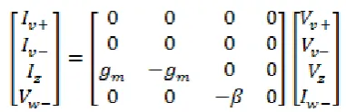
Port relation of VDIBA is described by the following matrix:
Where, β and gm describe the voltage gain and transconductance of VDIBA respectively. The value of β ideally
is unity. It can be seen that port z current is controlled by transconductance parameter gm which in turn is
controlled by the bias current (IB).
The CMOS implementation of the VDIBA is showing in Fig.3. The circuit consists an active loaded
differential pair (transistors M1 and M4) followed by a unity gain inverting voltage buffer (IVB) (matched
Fig. 3: CMOS structure of VDIBA
III. PROPOSED UNIVERSAL FILTER
Fig. 4 shows the proposed multi input signal output (MISO) voltage mode (VM) universal filter. It comprises
two capacitors and two VDIBA. It is three inputs and one output device. Proposed filter configuration realizes
all the responses in inverting and non- inverting modes. The biquad filters have property of low output
impedance which is an essential factor for cascadability for VM circuit
Fig. 4: Proposed VM biquad filter
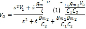
The output voltage of the proposed filter can be given as:
It can be viewed from (1) that all the filter function can be realized by the design filter from the same topology
without the requirement of any component matching condition.
From (1), the natural frequency is given as
Subsequently, the quality factor is given as
(1)
Bandwidth is given as
It is evident from (2a) and (2b) that the natural frequency and quality factor can be electronically tuned via 𝑔m.
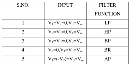
Table I shows realization condition for various input combinations for all filter functions
Table I: Input set for different filter functions
S.NO. INPUT FILTER
FUNCTION
1 V1=V2=0,V3=Vin LP
2 V2=V3=0,V1=Vin HP
3 V1=V3=0,V2=Vin BP
4 V2=0,V1=V3=Vin BR
5 V1=(-V2)=V3=Vin AP
It can be seen from (1) that BW and ω0 of proposed filter can be tuned independently by first setting the BW by
gm2 and then varying ω0 by gm1. The value of Q can be set by capacitance ratio C2/C1. The analysis of sensitivity
with respect to active and passive element for the proposed filter is less than 1.
Sensitivity of the above equation is given below:
IV. COMPARISON
The proposed filter configuration is compared with previously designed filters in Table II on the basis of
following important features such as (1)Independently tuned filter parameter (2) Appropriate input port
impedance (high-for voltage, Low for current Grounded/floating) (3) Appropriate output port
impedance-(Low-for voltage, High impedance-(Low-for current) (4) Component Matching constraints (5) No of resistors (Grounded/ floating) (6)
No of capacitors (Grounded/ floating) (7) No of filter functions –Low pass, High pass, Band pass, Band stop,
All pass (8) Mode of operation (CM/VM) (9) No of active elements with name.
It can be viewed that the designed filter provides better features, as compared to the other filters listed in Table
II, which lacks one or more important features.
(2b)
(2c)
V. SIMULATION RESULTS
To validate the proposed configuration, simulation results are presented in this section using Tanner EDA tool.
Supply voltage is set to 0.9V. The aspect ratios of the OTA transistors (M1-M4) and the IVB (M5 and M6) has
been taken as W/L (M1-M4)=18µm/1.08µm and W/L(M5,M6)=54μm/0.18μm. The transconductance (gm1, gm2)
of VDIBA has set to 656.01μA/V. The bias currents has been selected as IB =100 μA. The value of passive
components C1 and C2 is taken as 10pf and 5pf respectively. The transconductance are controlled by bias
currents of VDIBA. Fig. 5 and 6 depict the simulated filter responses of LP, BP, HP, BR and AP. Selected
component values results in Q = 0.707, f0= 3.41MHz and 3.53MHz, and BW= 15MHz for equal bias current i.e.
for gm1 and gm2. These result, thus confirms the validity of designed filter.
At Ib=100 A the frequency is 3.41MHz.
Fig.5: Frequency response of proposed universal filter
At Ib =150 the frequency is 3.53MHz. Features/
References
1 2 3 4 5 6 7 8 9
1 N N N N 0/1 0/2 5 VM 1(VDIBA)
2 Y Y N Y 0/1 0/2 5 VM 1 (VDIBA)
3 N N N N 0/1 0/2 5 VM 1(VDIBA)
4 Y Y N Y 0/2 2/0 5 VM 2(VDTA)
5 N N N N 0/0 2/0 3 VM 1(VDTA)
6 Y N N Y 1/0 2/0 5 VM 1(VDTA)
7 N Y N Y 0/0 2/0 5 CM 1(VDTA)
Fig.6: Frequency response of proposed universal filter
VI. CONCLUSION
The proposed circuit uses two capacitors and two VDIBAs only. The circuit has the capability to realize all the
functions of the filter without modifying circuit topology. The circuit has independent electronic tuning between
pole frequency and Bandwidth. Moreover, the configuration requires no component matching constraints and
has low active and low passive sensitivities. The performance of the designed circuit is verified by tanner
simulations using 180nm technology.
REFERENCES
[1] K.L.Pushkar, D.R. Bhaskar, Dinesh Prasad, 2014, “Voltage mode new universal biquad filter
configuration using a single VDIBA”, Circuits Syst Signal Process –springer, Vol. 33, pp. 275–285.
[2] Supachai Klungtong, Dusit Thanapatay, and Winai Jaikla, 2017, “Three-Input Single-Output
Voltage-Mode Multifunction Filter with Electronic Controllability Based on Single Commercially Available IC”
Active and Passive Electronic Components, Vol.2017, pp.1-11.
[3] Norbert Herencsar, Oguzhan Cicekoglu, Roman Sotner, Jaroslav Koton, Kamil Vrba, 2013, “New
resistorless tunable voltage-mode universal filter using single VDIBA”, Analog Integr Circ Sig Process –
springer, Vol. 76 pp.251–260.
[4] Jetsdaporn Satansup, Tattaya Pukkalanum, Worapong Tangsrirat, 2013, “Electronically tunable
single-input five-output voltage mode universal filter using VDTA and grounded passive elements”, Circuits
Syst Signal Process –springer, Vol. 27,pp .673–682.
[5] Abdullah Yesil, Firat Kacar, Hakan Kuntman, 2011, “New simple CMOS realization of voltage
differencing Transconductance amplifier and its RF filter application”, Radioengineering, Vol. 20, pp.
632-637.
[6] Dinesh Prasad, Data Ram Bhaskar,Mayank Srivastava, 2013, “Universal Current-Mode Biquad Filter
Using a VDTA”, Circuits and Systems, Vol. 4, pp.29-33.
[7] Jetsdaporn Satansup, Worapong Tangsrirat, 2014, “Compact VDTA based current mode electronically
pp.613-[8] B. Metin, “Electronic Tunability in Analog Filters, 2007,” Ph.D. Thesis, Bogazici University, Istanbul.
[9] Norbert Herencsar, Jaroslav Koton, Shahram Minaei, Erkan Yuce, and Kamil Vrba, 2013, “Novel
Resistorless and electronically tunable realization of Dual-Output VM All-Pass Filter using VDIBA”,
Analog Integr Circ Sig Process –springer, Vol. 74 , pp.141–154.
Sarita Pal (M.Tech scholar) received the degree of B.Tech in Electronics and communication engineering from Bundelkhand University, Jhansi (U.P.) in 2012. Her
areas of interest are design of analog signal processing circuits and low power CMOS
VLSI design pursuing M.Tech. at A.K.G Engineering College, Ghaziabad (U.P.).
Devesh Singh received the degree of B.Tech. in Electronics and Communication from Institute of Engineering & Technology, Jaunpur and degree of M.E in
Communication System from Jabalpur Engineering College, Jabalpur, India in
2001 and 2005 respectively. He received his Ph.D from Department of Electronics
and Communication Engineering, Jamia Millia Islamia, New Delhi. He is working
as an Assistant Professor in A.K.G. Engineering College, Ghaziabad as since
2005. He has published five papers in various international journals and