c e-ISSN: 2348-6848, p- ISSN: 2348-795X Volume 3, Issue 01, January 2016
International Journal of Research (IJR)
Available at http://internationaljournalofresearch.orgFuzzy Logic Based Closed loop control scheme for Voltage
doublers based DC – DC Converter
M.Mohan
1& S.Raj shekar
2 1M.Tech Scholar,Dept. of EEE, ASR College of Engineering and Technology, JNTUK, A.P
2Assistant Professor, Dept. of EEE, ASR College of Engineering and Technology, JNTUK, A.P
Abstract: —
The paper proposes a high step up boost converterwith coupled-inductor and voltage-doubler circuits is proposed. The proposed converter has used a coupled inductor with switched capacitors. The capacitors were made to get charged in parallel and were made to get discharged in series by the configuration to achieve high step up voltage gain. And the voltage across the load is maintained constant by using a closed loop control.Switch voltage stress and the circulating current are reduced by a clamp circuit which is composed of a diode followed by a capacitor. Thus the efficiency of the converter is improved. The operating principle and the steady state analysis are discussed in detail. A Fuzzy logic controller is designed such that it eliminates the Voltage Drift problemComputer simulation by MATLAB/ SIMULINK hasbeen used to support the developed concept.
Keywords: Coupled Inductor; FLC; Switched Capacitor circuit; Switched Capacitor; PI Controller; Fuzzy Logic Controller
I.
INTRODUCTION
Boost converter is one of the most important and widely used devices of modern powerapplications. These converters are electronic devices used to change DC electrical power efficiently from one voltage level to another. They provide smooth acceleration control, high efficiency, and fast dynamic response. There are FOUR main types of converter usually called the buck, boost, buck-boost and Boost converters. The buck converter is used for voltage stepdown/reduction, while the boost converter is used for voltage step-up. The buck-boost and Cuk converters can be used for either step-down or step-up.
Basically, the DC-DC converter consists of the power semiconductor devices which are operated as electronic switches and classified as switched mode DC-DC converters. Operation of the switching devices causes the inherently nonlinear characteristic of the DC-DC converters. Due to this unwanted nonlinear
characteristics, the converters requires a controller with a high degree of dynamic response. Pulse Width Modulation (PWM) is the most frequently consider method among the various switching control method. In DC-DC voltage regulators, it is important to supply a constant output voltage, regardless of disturbances on the input voltage.
Nowadays, the control systems for many power electronic appliances have been increasing widely. Crucial with these demands, many researchers or designers have been struggling to find the most economic and reliable controller to meet these demands. The idea to have a control system in dc-dc converter is to ensure desired voltage output can be produced efficiently as compared to open loop system. Controller for the PWM switching control is done by Fuzzy Logic Controller.
Many different methods have been proposed to improve the efficiency of the converter and to achieve high voltage gain, which can be done by using a switched capacitor and a coupled inductor is used for high gain by adjusting its turns ratio. Voltage spikes may occur due to the coupled inductor. For which we have used an active clamp circuit with coupled inductor which avoids voltage spikes.
c e-ISSN: 2348-6848, p- ISSN: 2348-795X Volume 3, Issue 01, January 2016
International Journal of Research (IJR)
Available at http://internationaljournalofresearch.orgended scheme cost is reduced. Galvanic isolation is needed, but suitable only for low power and frequency applications [13], [14]. In this converter no need of extreme duty ratio but if conduction losses or switching losses occurs the efficiency is reduced [11]. It is possible to generate the non-isolated dc-dc converters but the major drawback is that switching frequency must be maintained constant and the turn ratio of the auto transformer must be unity [11]. Some converters operate at very high frequency with fast transient response. The main switch is fabricated from an integrated power process, the layouts can be changed to vary the parasitic, however design of switch layout is complex, fixed frequency and constant duty ratio must be maintained [12]. This converter provides high voltage gain and can be employed for high power applications however the duty ratio is limited to 0.85 [8], [9]. In this, the energy of the leakage inductor is recycled to the output load directly, limiting the voltage spike on the main switch. To achieve a high step-up gain, it has been proposed that the secondary side of the coupled inductor can be used as flyback and forward converters [10], [10].In some converters voltage gain is improved through output voltage stacking [12].
Fig.1. Proposed Block Diagram.
The main objective is to improve the Voltage Gain of the Step-up Converter and also to reduce Voltage stress of the circuit. Further the Voltage Drift problem is reduced using closed loop control of the proposed converter with fuzzy logic controller. From Fig.1, The output voltage from the converter is fed as feed back to the FLC; there it compares the feedback voltage signal and the reference voltage signal to produce PWM pulse which triggers the main switch of the converter.
A conventional high step-up dc–dc converter with a coupledinductor technique is shown in Fig.1 [21]. The structure of this converter is very simple, and the leakage-inductor energy of the coupled leakage-inductor can be recycled to
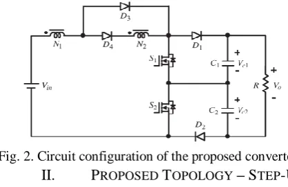
the output. However, the voltage stresses on switch S1 and diode D1, which are equal to the output voltage, are high. This paper presents a novel high step-up dc-dc converter, as shown in Fig. 2. The coupled-inductor and voltage-doubler techniques are integrated in the proposed converter to achieve high step-up voltage gain. The features of this converter are as follows:
1) The leakageinductor energy of the coupled inductor can be recycled;
2) The voltage stresses on the switches are half the level of the output voltage; thus, the switches with low voltage rating andlow ON-state resistance RDS(ON) can be selected; 3) The voltage gain achieved by the proposed converter is double that of the conventional high step-up converter; under the same voltage gain and duty ratio, the turns ratio of the coupled inductor for the proposed converter can be designed to be less than that of the conventional high step-up converter; and
4) The frequency of the magnetizing-inductor current for the proposed converter is double the switching frequency. Thus, the magnetizing inductance of the coupled inductor for the proposed converter can be designed to be less than that of the conventional high step-up converter under the same switching frequency
Fig. 2. Circuit configuration of the proposed converter
II. PROPOSED TOPOLOGY – STEP-UP
DC-DCCONVERTER
c e-ISSN: 2348-6848, p- ISSN: 2348-795X Volume 3, Issue 01, January 2016
International Journal of Research (IJR)
Available at http://internationaljournalofresearch.orgvoltages across C1 and C2 are considered to be constant during one switching period
Fig.3. Simplified diagram of proposed diagram
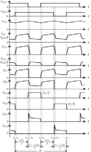
Fig. 4 shows some typical waveforms during one switching period in continuous-conduction-mode (CCM) operation. The operating principle is described as follows.
Fig.4.Some typical waveforms of the proposed converter at CCM operation.
1. Mode I [t0,t1]: At t = t0, S1 and S2 are turned on. The current-flow path is shown in Fig. 5(a). The dc-source energy is transferred to Lm and Lk1 through D3, S1, and S2, so currents iLm, iLk1, and iD3 are increased. The energy stored in Lk2 is released to Lm and Lk1 through D4, S1, and S2. Thus, iLk2 is decreased. Meanwhile, the energy stored in Lk2 is recycled. The energy stored in CS2 is rapidly and completely discharged. The energies stored in C1 and C2 are discharged to the load. This mode ends when iLk2 is equal to zero at t = t1.
2. Mode II [t1,t2]: In this mode, S1 and S2 are still turned on. The current-flow path is shown in Fig. 5(b). The
dcsource energy is still transferred to Lm and Lk1. Thus, iLm and iLk1 are still increased. The energies stored in C1 and C2 are still discharged to the load.
3. Mode III [t2,t3]: At t = t2, S1 is turned off, and S2 is still turned on. The current flow path is shown in Fig. 5(c). The dc source energy is still transferred to Lm, Lk1, and CS1. Meanwhile, the voltage across S1 is increased rapidly. Theenergies stored in C1 and C2 are still discharged to the load.
4. Mode IV [t3,t4]: During this time interval, S1 is still turned off, and S2 is still turned on. The current-flow path is shown in Fig. 5(d). The dc source, Lm, and Lk1 areseries connected to transfer their energies to Lk2, C1, and the load. Thus, iLm and iLk1 are decreased, and iLk2 is increased. Meanwhile, the energy stored in Lk1 is recycled to C1 and the load. The energy stored in C2 is still discharged to the load. This mode ends when iLk1 is equal to iLk2 at t = t4.
5. Mode V [t4,t5]: During this period, S1 is still turned off, and S2 is still turned on. The current-flow path is shown in Fig. 5(e). The dc source, Lm, Lk1, and Lk2 are series connected to transfer their energies to C1 and the load. Thus, iLm, iLk1, and iLk2 are decreased. The energy stored in C2 is still discharged to the load.
6. Mode VI [t5,t6]: At t = t5, S1 and S2 are turned on. The current-flow path is shown in Fig. 5(f). The dc-source energy is transferred to Lm and Lk1 through D3, S1, and S2. Therefore, currents iLm, iLk1, and iD3 are increased. The energy stored in Lk2 is released to Lm and Lk1 through D4, S1, and S2. Thus, iLk2 is decreased. Meanwhile, the energy stored in Lk2 is recycled. The energy stored in CS1 is rapidly and completely discharged. The energies stored in C1 and C2 are discharged to the load. This mode ends when iLk2 is equal to zero at t = t6.
7. Mode VII [t6,t7]: During this time interval, S1 and S2 are still turned on. The current-flow path is shown in Fig. 5(g). The dc-source energy is still transferred to Lm and Lk1. Thus, iLm and iLk1 are still increased. The energies stored in C1 and C2 are still discharged to the load.
8. Mode VIII [t7,t8]: At t = t7, S1 is still turned on, and S2 is turned off. The current-flow path is shown in Fig. 5(h). The dc-source energy is still transferred to Lm, Lk1, and CS2. Meanwhile, the voltage across S2 is increased rapidly. The energies stored in C1 and C2 are still discharged to the load.
c e-ISSN: 2348-6848, p- ISSN: 2348-795X Volume 3, Issue 01, January 2016
International Journal of Research (IJR)
Available at http://internationaljournalofresearch.orgto C2 and the load. The energy stored in C1 is still discharged to the load. This mode ends when iLk1 is equal to iLk2 at t = t9.
c e-ISSN: 2348-6848, p- ISSN: 2348-795X Volume 3, Issue 01, January 2016
International Journal of Research (IJR)
Available at http://internationaljournalofresearch.orgFig. 5. Current-flow path of the operating modes during one switching period at CCM operation (a) Mode 1. (b) Mode 2. (c) Mode 3. (d) Mode 4. (e) Mode 5. (f) Mode 6.
(g) Mode 7. (h) Mode 8. (i) Mode 9. (j) Mode 10.
Mathematical calculation of paramaeters , which are used in this papers is given in Appendix section .
Assumptions to simplify the circuit analysis,
1. Capacitors C1, C2, C3 and C0 are large enough. And so, VC1, VC2, VC3 and VC0 are considered as constants in one switching period. 2. The power devices are ideal. 3. The coupling coefficient of the coupled inductor k isequal to Lm/ (Lm+Lk), and the turn ratio of the coupled inductor n is equal to Ns/Np.
III. FUZZY LOGIC CONTROLLER
The block diagram of fuzzy logic controller (FLC) is shown in fig.6. It consists of three main blocks: fuzzification, inference engine and defuzzification. The two FLC input variables are the error E and change in error E*. Depending on membership functions and the rules FLC operates.
Fig.6. Block Diagram of FLC
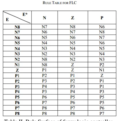
Table.II. shows the shows the representation of the typical Rule Surface of fuzzy logic controller.
Table.II. Rule Surface of fuzzy logic controller
IV. MATLAB BASED SIMULATION &RESULTS To verify the feasibility of the proposed system a simulink model is developed. Fig.6&Fig.7.shows the sub system in the simulink model.
Fig.6.MATLAB based simulation diagram of proposed system with masked diagrams
c e-ISSN: 2348-6848, p- ISSN: 2348-795X Volume 3, Issue 01, January 2016
International Journal of Research (IJR)
Available at http://internationaljournalofresearch.orgFig.8.MATLAB based simulation diagram of membership function-1 of proposed system
Fig.9.MATLAB based simulation diagram of membership function-2 of proposed system
Fig.10.MATLAB based simulation diagram of membership function-3 of proposed system
Fig.11.MATLAB based simulation diagram of proposed system-capacitors voltage
Fig.12.MATLAB based simulation diagram of proposed system –load current
Fig.13.MATLAB based simulation diagram of proposed system –load voltage
Fig.13. MATLAB based simulation diagram of proposed Fuzzy logic Controller system –error and change in error
TABLE.I: SIMULATION SPECIFICATIONS
Parameter Rating
Input dc voltage 24 V
Output dc voltage 200 V
Maximum output
power
250 W
Switching frequency 25 kHz
c e-ISSN: 2348-6848, p- ISSN: 2348-795X Volume 3, Issue 01, January 2016
International Journal of Research (IJR)
Available at http://internationaljournalofresearch.orgC2 = 47 μF
Coupled inductors Lm = 48 μH
CONCLUSION
Here a high step-up boost converter using coupled inductor with proportional integral control is simulated.In this paper a high step-up dc-dc converter for distributed power generation is discussed. By using the capacitor charged in parallel and discharged in series by the coupled inductor this converter provide high step-up voltage gains and high efficiency. It also has low input current ripple and low conduction losses, making it suitable for high power applications. The turn ratio of the coupled inductor is 1:4, but the output voltage of the converter is 16 times greater than the input voltage. The converter transfers the capacitive and inductive energy simultaneously to increase the total power delivery. By the capacitor charged in parallel and discharged in series by the coupled inductor, high step-up voltage gain is achieved. As the output voltage of the converter with FLC has minimum overshoot and produces a constant output current shows the better performance compared to the converter with PI controller.These studies could solve many types of problems regardless on stability because as we know that fuzzy logic controller is an intelligent controller to their appliances. Additionally, the switchvoltage stress is reduced, thus a switch with low voltage ratings can be selected.
REFERENCES
[1] T.F. Wu, Y.S. Lai, J.C. Hung and Y.M. Chen, ―Boost Converter with Coupled Inductors and Buck– Boost Type of Active Clamp‖ IEEE Trans Ind. Electron.,vol. 55, no. 1, Jan. 2008.
[2] B. Axelrod, Y. Berkovich and A.Ioinovici, ―Switched Capacitor/Switched-Inductor Structures for Getting Transformerless Hybrid DC–DC PWM Converters‖, IEEE TransCircuits And Systems—I: Regular Papers, Vol. 55, no. 2, Mar 2008.
[3] D. Sabin and A. Sundaram, "Quality enhances reliability," IEEE Spectrum, vol. 33, no. 2, Feb. 1996, pp. 34-41.
[4] R.J. Wai, C.Y. Lin, C.Y. Lin, R.Y. Duan and Y.R. Chang, ―High Efficiency Power Conversion System for Kilowatt-Level StandAlone Generation Unit with Low Input Voltage‖, IEEE Trans Ind.Electron., vol. 55, no. 10, Oct 2008.
[5] G.S. Yang, T.J. Liang and J.F. Chen, ―Transformerless DC–DC Converters With High Step-Up Voltage‖, IEEE Trans Ind.Electron., vol. 56, no. 8, Aug 2009.
[6] J.M. Burkhart, R. Korsunsky, and D.J. Perreault, ―Design Methodology For A Very High Frequency Resonant Boost Converter‖, IEEE Trans. Power Electron., vol. 28, no. 4, Apr 2013.
[7] F.S. Garcia, J.A. Pomilio and G. Spiazzi, ―Modeling and Control Design of the Interleaved Double Dual Boost Converter‖, IEEETrans Ind. Electron.,vol. 60, no. 8, Aug 2013.
[8] F.H. Dupont, C. Rech, R. Gules and J. R. Pinheiro, ―Reduced Order Model and Control Approach for the Boost Converter With a Voltage Multiplier Cell‖, IEEE Trans Power Electron.,vol. 28, no. 7, July 2013.
[9] R. J. Wai and R. Y. Duan, ―High step-up converter with coupled inductor,‖ IEEE Trans. Power Electron., vol. 20, no. 5, pp. 1025–1035, Sep. 2005.
[10] R. J. Wai, L. W. Liu and R. Y. Duan, ―High efficiency voltageclamped dc–dc converter with reduced reverse-recovery current and switch voltage stress,‖ IEEE Trans. Ind. Electron.., vol. 53, no. 1, pp. 272–280,Feb. 2005.
[11] J. W. Baek, M. H. Ryoo, T. J. Kim, D. W. Yoo and J. S. Kim, ―High boost converter using voltage multiplier,‖ in Proc. IEEEIECON, 2005, pp. 567–572.
[12] S.K. Changchien, T.J Liang, J.F. Chen and L.S. Yang, ―Novel High Step-Up DC–DC Converter for Fuel Cell Energy Conversion System‖, IEEE Trans Ind. Electron., vol. 57, no. 6, June 2010.
[13] Y. Zhao, Y. Deng and Xiangning, ―Interleaved Converter with Voltage Multiplier Cell for High Step-Up and High Efficiency Conversion‖, IEEE Trans. Power Electron., vol. 25, no. 9, Sep 2010.