Coupled Inductor Based SIMO Interleaved
Step-down Converter
Geethu Venugopal1, Saritha Sathyan2,
PG Student [PE], Dept. of EEE, Sree Narayana Gurukulam College of Engineering, Kadayiruppu, Kerala, India1 Associate Professor, Dept. of EEE, Sree Narayana Gurukulam College of Engineering, Kadayiruppu, Kerala, India2
ABSTRACT: This paper proposes a new coupled inductor based SIMO interleaved step down converter. Multiple output converters are widely used in industrial applications. Designing multi-output converters presents a remarkable challenge for the power supply designers. Converters utilizing a single primary power stage and generating more than one isolated output voltage are called multi-output converters. The basic requirements are small size and high efficiency. This paper mainly investigates a high efficiency coupled inductor based single input multiple output (SIMO) interleavedstep down converter. The proposed converter can step down the voltage of high voltage dc bus generated by the rectifier of an AC utility power to a controllable output voltage of different levels. The interleaved topology of the proposed converter can achieve high step down conversion ratio, high efficiency power conversion and reduced voltage ripples across the load.
KEYWORDS: SIMO, interleaved topology, coupled inductor.
I.INTRODUCTION
The proposed coupled inductor based single input multiple output interleaved step down converter is used to convert the bus voltage in to voltages of three different levels. The basic requirements of multi output converters are small size and high efficiency. Multi stage converter includes several power conversion stages between the PV cell and load of the system. Power conversion stages include DC-DC converter, DC-AC converter, step up converter etc. In this paper the proposed converter utilizes three power switches with different switching frequencies. The proposed system utilizes two coupled inductors. Coupled inductors are actually a pair of inductors and are coupled together so the input to one will result in the output of both. Here the leakage inductor energy of the coupled inductor can be recycled, and the voltage spikes on the power switches can be alleviated. Therefore the objectives of high efficiency power conversion, high step down conversion ratio, and various output voltages with different levels can be obtained.
In addition to paralleling the converters, the interleaving topology can achieve several benefits. Interleaved converters have simple structure and low control complexity. So it can use in applications where, non-isolation and high output current with low ripples are required. Interleaving topology connects one or more converters in parallel to share the power flow between the conversion chains. The main advantage of this topology is reduction in size, weight and volume of inductors and capacitors. And also it can achieve significant reduction of current and voltage ripples. In this proposed converter higher efficiency is realized by splitting the output current into different paths, substantially reducing losses and inductor AC losses in the field of power electronics.
II.LITERATURE REVIEW
ISSN (Print) : 2320 – 3765 ISSN (Online): 2278 – 8875
I
nternational
J
ournal of
A
dvanced
R
esearch in
E
lectrical,
E
lectronics and
I
nstrumentation
E
ngineering
(An ISO 3297: 2007 Certified Organization)
Vol. 5, Issue 9, September 2016
al. The circuit achieves completed coupling from the input so that the mutual effects between modules are eliminated and thus oscillations are avoided. The converter can achieve satisfactory comprehensive performance when the step-up ratio is low and smooth transition is achieved since the circuit has no nonlinear dc gain. L. Gu, K. Jin, et al present a family of switching capacitor regulators. In conventional PWM converters, the dynamic performance is limited by the inductor. Switching capacitor converters utilize the capacitor as the energy transmitter and have good transient response. However, their output voltage cannot be regulated by the duty cycle. H. L. Do proposes zero-voltage-switching synchronous buck converter with a coupled inductor. An additional winding of the filter inductor and a diode are adopted to achieve ZVS turn-on of the power switches and alleviate the reverse recovery problem of the body diode of the synchronous switch. It can achieve a ZVS turn-on of two power switches while maintaining CCM.
III.SYSTEM MODEL AND WORKING
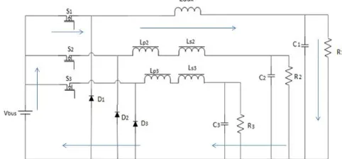
The proposed coupled inductor based SIMO interleaved step down converter is shown in figure1. Here the converter can step-down the voltage of a high-voltage DC bus generated by the rectifier of an AC utility power to controllable three different voltages. The proposed converter has three switches S1, S2, S3 with different switching frequencies.
These switches can on and off according to the modes of operation. The circuit consists of two coupled inductors and an auxiliary inductor. LP1 and LS1 represent the individual inductors in the primary and secondary of the first coupled
inductor. LP2 and LS2 represent the individual inductors in the primary and secondary of the second coupled inductor.
Laux is the auxiliary inductor. D1, D2, D3 are the freewheeling diodes. C1, C2, C3 are the filter capacitors across the
output loads R1, R2, R3respectively.Vbus is the input bus voltage. The voltages across RO1, RO2, RO3 are VO1, VO2, VO3
respectively.
Fig. 1 coupled inductor based SIMO interleaved step down converter
The coupled inductor based SIMO interleaved step down converter has six modes of operation. The switches S1, S2, S3
are on and off according to these modes. MODE 1
Fig. 2 Mode 1 operation of coupled inductor based SIMO interleaved step down converter
The mode 1 operation starts when the switch S1 is turned on. When the switch S1 is on, the current i1 starts to flow
through the auxiliary inductor Laux, R1. The path is shown in figure 2. During this mode the output voltage VO1 is
obtained across the load R1.
Fig. 3 Mode 2 operation of coupled inductor based SIMO interleaved step down converter
This mode starts when the switch S1 is turned off. So the current freewheels through the diode D1 through the path as
shown in figure 3. MODE 3
Fig. 4 Mode 3 operation of coupled inductor based SIMO interleaved step down converter
Mode 3 starts when the switch S2 is turned on. So the current i2 flows through the primary winding Lp2 and the
secondary winding Ls2 of the coupled inductor and R2 of the proposed system. During this mode the output voltage VO2
is obtained across the load R2.
MODE 4
Fig. 5 Mode 4 operation of coupled inductor based SIMO interleaved step down converter
When the switch S2 is turned off, the mode 4 starts. During this mode the current freewheels through the diode D2 as
ISSN (Print) : 2320 – 3765 ISSN (Online): 2278 – 8875
I
nternational
J
ournal of
A
dvanced
R
esearch in
E
lectrical,
E
lectronics and
I
nstrumentation
E
ngineering
(An ISO 3297: 2007 Certified Organization)
Vol. 5, Issue 9, September 2016
MODE 5
Fig. 6 Mode 5 operation of coupled inductor based SIMO interleaved step down converter
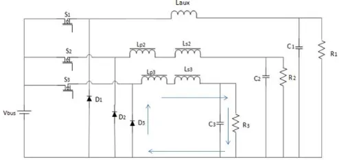
This mode starts when the switch S3 is turned on. When the switch S3 is turned on, the current i3 flows through the
primary winding Lp3, secondary winding Ls3 of the coupled inductor and the load R3 of the proposed system as shown
in the figure 6. MODE 6
Fig. 7 Mode 6 operation of coupled inductor based SIMO interleaved step down converter
During this mode of operation the current freewheels through the diode D3. Mode 6 operation is shown I the figure 7.
IV.SIMULATION
The simulation result was done in MATLAB/Simulink. The Simulink model of the coupled inductor based SIMO interleaved step down converter is shown in the figure 8. The output voltage waveforms with different levels are obtained. The gate pulses generated for turn on/off of the switches are plotted. Closed loop control is adopted for the proposed system.
Fig. 8 Simulink model of the coupled inductor based SIMO interleaved step down converter
Here the proposed converter outputs are designed for 12V, 80V, and 96V. The input bus voltage is taken as 150 V. The gate pulses generated for the switches S1, S2, S3 are shown in the figure 9 and 10.
Fig. 9 Gate pulses for the switch S1and S2
The switching frequency designed for the switch S1 is 2K and for the switch S2 is 4K.
ISSN (Print) : 2320 – 3765 ISSN (Online): 2278 – 8875
I
nternational
J
ournal of
A
dvanced
R
esearch in
E
lectrical,
E
lectronics and
I
nstrumentation
E
ngineering
(An ISO 3297: 2007 Certified Organization)
Vol. 5, Issue 9, September 2016
The output waveforms are given in the figures 11. VO1, VO2, VO3 are designed for 12V, 80V and 96V respectively. By
using PI control we can reduce the peak overshoot.
Fig. 11 Simulation result of output voltages of coupled inductor based SIMO interleaved step down converter
V.HARDWARE IMPLEMENTATION
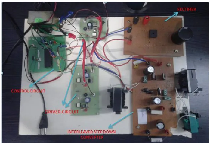
Hardware implementation of the proposed coupled inductor based SIMO interleaved step down converter is given in the figure 12.
Fig. 12 Hardware implementation of the coupled inductor based SIMO interleaved step down converter
Fig. 13 VO1 of the coupled inductor based SIMO interleaved step down converter
VO1 of the coupled inductor based SIMO interleaved step down converter is shown in the figure 13. VO1 is designed for
12 V.
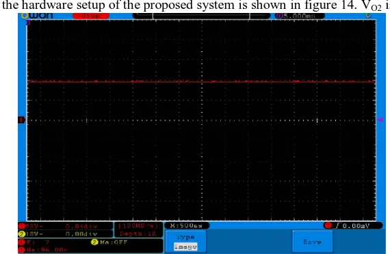
Fig. 14 VO2 of coupled inductor based SIMO interleaved step down converter
The VO2 obtained from the hardware setup of the proposed system is shown in figure 14. VO2 is designed for 80 V.
ISSN (Print) : 2320 – 3765 ISSN (Online): 2278 – 8875
I
nternational
J
ournal of
A
dvanced
R
esearch in
E
lectrical,
E
lectronics and
I
nstrumentation
E
ngineering
(An ISO 3297: 2007 Certified Organization)
Vol. 5, Issue 9, September 2016
VO3 of coupled inductor based SIMO interleaved step down converter is shown in the figure 15. VO3 is designed for
96V.
VI. RESULT AND DISCUSSION
The proposed step down converter is shown in the figure 1 and its Simulink model and hardware setup are given in figure 8 and 12.We simulate the system using PI control. We get the simulation results which are given in the figures 9,10 and 11.Then we implement the hardware. The results obtained from the hardware setup of the coupled inductor based SIMO step down converter are given in figures 13, 14, 15. The outputs designed for the proposed system are 12V, 80V, 96V.
VII.CONCLUSION
Coupled inductor based SIMO interleaved step down converter is proposed in this paper. This converter has three output voltages of three different levels. The proposed converter achieves high step down conversion ratio. The interleaved topology adds additional benefits such as reduced voltage ripple in the output load. It also reduces the capacitor size. Experimental results are provided to confirm the converter operation in reference to SIMO operation.
REFERENCES
[1] S. S. Lee, “Step-down converter with efficient ZVS operation with load variation,” IEEE Trans. Ind. Electron., vol. 61, no. 1, pp. 591-597. Jan. 2014.
[2] H. L Do, “A Zero voltage switching synchronous buck converter with a coupled inductor,” IEEE Trans. Ind. Electron., vol. 58, no.8, pp. 3440=3447, Aug. 2011.
[3] Rong-Jong Wai, and Jun-JieLiaw “High Efficiency coupled inductor based step down converter” IEEE Trans. Power Electron.,vol. 30,no.7, pp. 3638-3649, Jul.2015.
[4] R. G. Wandhare and V. Agarwal, “Novel integration of a PV wind energy system with enhanced efficiency,” IEEE Trans. Power Electron., vol.30,no.7, pp.3638-3649.
[5] K. Xie, Z. Jiang, and W. Li, “Effect of wind speed on wind turbine power converter reliability,” IEEETrans. Energy Convers., vol. 27, no.1pp. 96-104, Mar. 2012.
[6] K. W. Hu and C. M. Liaw, “Development of a wind interior permanent magnet synchronous generator-based microgrid and its operation control,”IEEE Trans. Power Electron., vol. 30, no. 9, pp. 4973–4985, Sep. 2015.
[7] F. Blaabjerg and K. Ma, “Future on power electronics for wind turbine systems,” IEEE J. Emerg. Sel. Topics Power Electron., vol. 1, no. 3,pp. 139–152, Sep. 2013.
[8] J. Xu, S. Liao, Y. Sun, X. Y. Ma, W. Gao, X. Li, J. Gu, J. Dong, and M.Zhou, “An isolated industrial power system driven by wind coal power for aluminum productions: A case study of frequency control,” IEEE Trans.Power Syst., vol. 30, no. 1, pp. 471–483, Jan. 2015.
[9] F. Forest, A. T. Meynard, J. J. Huselstein, D. Flumian, C. Rizet, and A. Lacarnoy, “Design and characterization of an eight-phase-137-Kw intercell transformer dedicated to multicell dc-dc stages in a modular UPS,” IEEE Trans. Power Electron., vol. 29, no. 1, pp. 45–55, Jan. 2014. [10] R. Santiago Maciel, L. C. de Freitas, E. A. Alves Coelho, J. B. Vieira, and L. C. Gomes de Freitas, “Front-end converter with integrated PFCand dc-dc functions for fuel cell UPS with DSP-based control functions,”IEEE Trans. Power Electron., vol. 30, no. 8, pp. 4175–4188, Aug. 2015.
[11] J. P. Rodrigues, S. A. Mussa,M. L.Heldwein, and A. J. Perin, “Three-level ZVS active clamping PWM for the dc-dc buck converter,” IEEE Trans.Power Electron., vol. 24, no. 10, pp. 2249–2258, Oct. 2009.
[12] Q. Du, B. Qi, T.Wang, T. Zhang, and X. Li, “A high-power input-parallel output-series buck and half bridge converter and control methods,”