ISSN: 2319-8753
I
nternational
J
ournal of
I
nnovative
R
esearch in
S
cience,
E
ngineering and
T
echnology
(An ISO 3297: 2007 Certified Organization)
Vol. 3, Issue 5, April 2014
Copyright to IJIRSET www.ijirset.com 12244
Efficient Implementation of Reconfigurable
MIMO Decoder Accelerator Chip
Lakshmi Priya.K
P.G. Student, Department of Electronics and Communication Engineering, PSNA College of Engineering and Technology,
Dindigul, Tamilnadu, India.
Abstract: In this paper I present an energy efficient reconfigurable MIMO (Multiple input Multiple output)decoder accelerator hardware architecture. It delivers full programmability across different wireless standards (i.e., WiFi, 3G-long term evolution, and WiMax) as well as different MIMO decoding algorithms (i.e., minimum mean square error, singular value decomposition, and maximum likelihood) with extreme energy efficiency. We propose an Hough transform architecture instead of CORDIC for the Rotation unit in the processing core . The energy efficiency of our MIMO accelerator chip was compared against existing programmable MIMO accelerator, it delivered energy efficiencies that were 5% less than the existing system.
Keywords: CORDIC, Hough Architecture, Reconfigurable MIMO (Multiple input Multiple output) decoder, Rotation
Unit.
I. INTRODUCTION
Multiple-input–multiple-output (MIMO) processing and orthogonal frequency division multiplexing (OFDM) are two dominant technologies in emerging wireless communications systems .MIMO is an antenna technology for wireless communications in which multiple antennas are used at both the source and destination to minimize errors and optimize data speed[1-5].In OFDM a wideband frequency selective fading channel is divided into several independent narrowband flat-fading sub channels. A MIMO decoder is the receiver component that separates the Nss transmitted data streams from the signals received on the Nrx receives antennas. The MIMO decoding operation is matrix and vector intensive. For an OFDM system, this processing is repeated for every sub channel. MIMO-OFDM techniques improve data rate and reliability. Several publications [6-13] report on various hardware designs and implementations for MIMO decoders. but these decoder designs use a single MIMO decoding algorithm such as zero forcing (ZF), minimum mean square error (MMSE)[6],[7]. maximum likelihood (ML) [8] or one of the many sphere decoding (SD) variants[9-11], Several reconfigurable MIMO decoders have been reported in the literature[10-12] .These designs are neither flexible enough to be tailored to a new standard.
ISSN: 2319-8753
I
nternational
J
ournal of
I
nnovative
R
esearch in
S
cience,
E
ngineering and
T
echnology
(An ISO 3297: 2007 Certified Organization)
Vol. 3, Issue 5, April 2014
Copyright to IJIRSET www.ijirset.com 12245 II. MIMO ACCELERATOR HARDWARE ARCHITECTURE
The MIMO accelerator architecture is shown in Fig 1. The main challenge in designing the memory map was providing a centralized data memory that allows general modes of access to data, independent of the algorithm,while maintaining the ability to provide the data vectors arranged in the correct order to and from the processing cores in a single cycle[16].The processing core is optimized for programmable processing of matrix operations necessary for linear MIMO decoders.
Fig.1.MIMO Accelerator basic block diagram
The MIMO accelerator is a complex number vector-based processor that works on complex vector operands of length Nrx —where Nrx is the number of receive antennas used in the MIMO system. Since most MIMO decoding algorithms can be broken down into a series of vector operations, the processor uses a vector as its smallest operand.
The processing core consists of four Processing units: 1. Matrix addition/Subtraction unit ,2.Inner product unit 3.Vector element- wise division unit and 4.Rotation unit. These operations are necessary and sufficient for coverage of major linear MIMO decoding algorithms [14].The number of units in each core is chosen to equalize the number of outputs and force them to be a multiple of the vector size.
ISSN: 2319-8753
I
nternational
J
ournal of
I
nnovative
R
esearch in
S
cience,
E
ngineering and
T
echnology
(An ISO 3297: 2007 Certified Organization)
Vol. 3, Issue 5, April 2014
Copyright to IJIRSET www.ijirset.com 12246
Fig.2.Matrix addition/subtraction unit Fig.3. Inner product unit
Second is a Inner product unit (Fig 3.) that contains four dot product blocks. Each of which computes a single complex number that results from a dot product of two complex Nrx vectors. ie Any combination of row and column multiplication operations on vectors, matrices or submatrices .This allows the multiplication unit to perform a complete vector-matrix multiplication in a single processor cycle. This multiplication unit is necessary for many MIMO decoding algorithms.Third is a reciprocal unit shown in Fig.4. that computes a reciprocal of Nrx real numbers. It is mainly used for scaling the signal power.
ISSN: 2319-8753
I
nternational
J
ournal of
I
nnovative
R
esearch in
S
cience,
E
ngineering and
T
echnology
(An ISO 3297: 2007 Certified Organization)
Vol. 3, Issue 5, April 2014
Copyright to IJIRSET www.ijirset.com 12247
III.ROTATION UNIT
The fourth processing unit is the rotation unit. It is the most power hungry unit in the processing core. Generally it consists of a group of coordinate rotation (CORDIC) blocks[18]. Here CORDIC is COordinate Rotation DIgital Computer, also known as the digit-by-digit method. It takes so many iterations to complete a single rotation so it consumes more power. This can be modified by using Hough architecture. It works based on line segment and produces a rotated sequence with reduced number of iteration [19]so the power consumption can be minimized .
IV.ROTATION UNIT USING HOUGH TRANSFORM
A block diagram of the proposed architecture is shown in Fig. 5. Run-length encoding is a simple process which reads the binary values from the input and output the{rb,code,zl}triplet. The PE is run-time configurable for computing Hough transform of any angles. Each PE calculates the consolidated ρθ values for all the input data where ρθ represents ρ value for a line with angle θ. The Vote Memory stores all the votes. Here we use both inter-block and intra-block incrementing in their PE. The inter-block incrementing shown in Fig.6. that calculates the ρθ(po) of first input where ρθ represents ρ value for a line with angle θ which passes through the point p. The intra-block incrementing calculates ρθ(x,y) values of other data s after the inter-block incrementing. Two accumulators can be used to implement the inter-block incrementing as shown in Fig. 6, where Nsinθ can be precomputed. In order to skip zero-blocks, a step-table is introduced in the proposed architecture. Col-reg calculates theρθ(po) values for the nonzero blocks in a block-row in the -direction every clock cycle, and row-reg calculates ρθ(po) values for the first blocks of block-rows in the -direction every time after a block-row processing is completed.
Fig.5.Hough transform rotation unit Fig.6.Inter block incrementing
ISSN: 2319-8753
I
nternational
J
ournal of
I
nnovative
R
esearch in
S
cience,
E
ngineering and
T
echnology
(An ISO 3297: 2007 Certified Organization)
Vol. 3, Issue 5, April 2014
Copyright to IJIRSET www.ijirset.com 12248 whole data, the eight votes in the memory addressed by the eight ρθ values will need to be accumulate . The computed ρθ(po) is divided into the integer part i0 and the fractional part f0 only the fractional part is used for calculating the vote-offsets as shown in Fig. 7. The first stage of Fig. 7 calculates the vote-vote-offsets V0i for the ith input The vote-vote-offsets range from 0 to 4, and are represented by 3-b numbers. These numbers are decoded by 3:8 decoders as shown in the second stage of Fig. 7. In Fig. 8, the outputs of the decoders are combined with the values of the corresponding input using a combination logic circuit to determine Vi, which represents the consolidated number of votes for each different vote-offset.
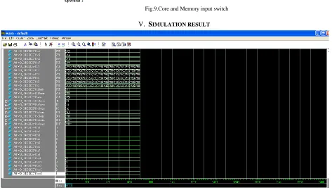
Core and memory input switch shown in Fig.9 have the ability to to provide the data vectors arranged in the correct order to and from the processing cores in a single cycle. This data is logically divided into a number of complex―matrix variables‖ of size Nrx by Nrx. When an instruction is executed for a subchannel, the chunk of data associated with the subchannel is retrieved and then delivered to the core-input switch. As shown in Fig.7. The core-input switch is a two level multiplexing circuit that selects and properly arranges the complex vectors needed by the processing core—whether they are row vectors, column vectors, matrix diagonals, or a combination thereof.
Fig.7.intra block increment Fig.8.Vote consolidation
ISSN: 2319-8753
I
nternational
J
ournal of
I
nnovative
R
esearch in
S
cience,
E
ngineering and
T
echnology
(An ISO 3297: 2007 Certified Organization)
Vol. 3, Issue 5, April 2014
Copyright to IJIRSET www.ijirset.com 12249 Fig.9.Core and Memory input switch
V. SIMULATION RESULT
Fig .10 Simulation result of Proposed rotation unit
Table.1 Power consumption comparison of rotation unit using cordic and hough architecture ROTATION UNIT CORDIC ARCHITECTURE HOUGH ARCHITECTURE
ISSN: 2319-8753
I
nternational
J
ournal of
I
nnovative
R
esearch in
S
cience,
E
ngineering and
T
echnology
(An ISO 3297: 2007 Certified Organization)
Vol. 3, Issue 5, April 2014
Copyright to IJIRSET www.ijirset.com 12250
Above Fig.10 shows the simulation result of rotation unit using hough architecture , the results vv1,vv2,vv3&vv4 shows the rotated value and the Table.10 shows the power consumption comparison of CORDIC and HOUGH architecture
VI.CONCLUSION
This paper presented the ASIC implementation of the reconfigurable MIMO accelerator . The accelerator is fully programmable within the domain of algorithms and functions needed to implement MIMO decoding (MMSE, SVD, QR, etc.) for any arbitrary system or standards (i.e., WiFi, LTE, etc.). The paper presented the hough architecture for the Rotation unit. The power consumption of this architecture was measured to be 151mw.. When compared this with the existing CORDIC architecture, the accelerator energy consumption was 5% less than the existing design.
REFERENCES
[1] A. J. Paulraj, D. A. Gore, R. U. Nabar, and H. Bolcskei, ―An overview of MIMO communications—A key to gigabit wireless,‖ Proc. IEEE, vol. 92, no. 2, pp. 198–218, Feb. 2004.
[2] IEEE Standard for Information Technology–Local and metropolitan Area Networks–Specific Requirements—Part 11: Wireless LAN Medium Access Control (MAC)and Physical Layer (PHY) Specifications Amendment 5: Enhancements for Higher Throughput, IEEE Standard 802.11n-2009, Oct. 2009. [3] IEEE Standard for Local and Metropolitan Area Networks Part 16: Air Interface for Broadband Wireless Access Systems Amendment 3: Advanced Air Interface, IEEE Standard 802.16m-2011, May 2011.
[4] M. Baker. (2009, Mar.). E-UTRA—LTE Physical Layer General Description [Online]. Available: http://www.in2eps.com/3g36/tk-3gpp- 36-201.html [5] M. Baker, ―LTE-advanced physical layer,‖ in Proc. IMT Ad. Evaluation Workshop, Dec. 2009, pp. 1–48.
[6] H. S. Kim, W. Zhu, J. Bhatia, K. Mohammed, A. Shah, and B. Daneshrad, ―A practical, hardware friendly MMSE detector for MIMO-OFDM based systems,‖ EURASIP J. Adv. Signal Process., vol. 2008, p. 94, Jan. 2008.
[7] J. Wang, ―A recursive least-squares ASIC for broadband 8 × 8 multipleinput multiple-output wireless communications,‖ Ph.D. dissertation, Henry Samueli School Eng. Appl. Sci., Univ. California Los Angeles, Los Angeles, CA, USA, 2005.
[8] M. Li, R. Fasthuber, D. Novo, B. Bougard, L. Van Der Perre, and F. Catthoor, ―Algorithm-architecture co-design of soft-output ML MIMO detector for parallel application specific instruction set processors,‖ in Proc. DATE, Apr. 2009, pp. 1608–1613.
[9] A. Burg, M. Borgmann, M. Wenk, M. Zellweger, W. Fichtner, and H. Bolcskei, ―VLSI implementation of MIMO detection using the sphere decoding algorithm,‖ IEEE J. Solid-State Circuits, vol. 40, no. 7, pp. 1566–1577, Jul. 2005.
[10] R. Shariat-Yazdi and T. Kwasniewski, ―A multi-mode sphere detector architecture for WLAN applications,‖ in Proc. IEEE Int. SOC Conf., Sep. 2008, pp. 155–158.
[11] C.-H. Yang and D. Markovic, ―A flexible DSP architecture for MIMO sphere decoding,‖ IEEE Trans. Circuits Syst. I, Reg. Papers, vol. 56, no. 10, pp. 2301–2314, Oct. 2009.
[12] C.-J. Huang, C.-W. Yu, and H.-P. Ma, ―A power-efficient configurable low-complexity MIMO detector,‖ IEEE Trans. Circuits Syst. I, Reg. Papers, vol. 56, no. 2, pp. 485–496, Feb. 2009.
[13] J. Eilert, D. Wu, and D. Liu, ―Implementation of a programmable linear MMSE detector for MIMO-OFDM,‖ in Proc. IEEE ICASSP, Apr. 2008, pp. 5396–5399.
[14] K. Mohammed and B. Daneshrad, ―A MIMO decoder accelerator for next generation wireless communications,‖ IEEE Trans. Very Large Scale Integr. (VLSI) Syst., vol. 18, no. 11, pp. 1544–1555, Nov. 2010.
[15] K. Mohammed, M. I. A. Mohamed, and B. Daneshrad, ―A parameterized programmable MIMO decoding architecture with a scalable instruction set and compiler,‖ IEEE Trans. Very Large Scale Integr. (VLSI) Syst., vol. 19, no. 8, pp. 1485–1489, Aug. 2011.
[16] Z.-Y. Huang and P.-Y. Tsai, ―Efficient implementation of QR decomposition for gigabit MIMO-OFDM systems,‖ IEEE Trans. Circuits Syst. I, Reg. Papers, vol. 58, no. 10, pp. 2531–2542, Oct. 2011.
[17] M. Shabany, D. Patel, and P. G. Gulak, ―A low-latency low-power QRdecomposition ASIC implementation in 0.13 μm CMOS,‖ IEEE Trans.Circuits Syst. I, Reg. Papers, vol. 60, no. 2, pp. 327–340, Feb. 2013.
[18] K. Mohammed and B. Daneshrad ― Energy Efficient Programmable MIMO Decoder Accelerator Chip in 65-nm CMOS ,‖ IEEE Trans. Very Large Scale Integr. (VLSI) Syst., vol. 70, no. 11, pp. 1544–1555, Nov. 2013.