Design of threshold logic gate using Testing Delay in
Current Mode
Perivemula Naga Padma Mounika Sri, K.Ranjith Kumar, Dr. P Prasanna Murali Krishna
[email protected] , [email protected]2, [email protected]3 1 Pg Scholar, VLSI, Krishnachaitanya Institute of Technology & Sciences, Markapur, Andhra Pradesh.
2 Assistant Professor, Dept Of Ece, Krishnachaitanya Institute Of Technology & Sciences,
Markapur,Andhra Pradesh.
3 Professor & HOD, Dept Of Ece, Krishnachaitanya Institute Of Technology & Sciences,
Markapur,Andhra Pradesh.
Abstract: Current mode is a popular CMOS-based
implementation of threshold logic functions, where the gate delay depends on the sensor size. The power of the threshold gate design style lies in the intrinsic complex functions implemented by such gates, which allow system realizations that require less threshold gates or gate levels than a design with standard logic gates. This paper presents a new implementation of current mode threshold functions for improved gate delay and switching energy. An analytical method is also proposed in order to identify quickly the sensor size that minimizes the gate delay. Simulation results on different gates implemented using the optimum sensor size indicates that the proposed current mode implementation method outperforms consistently the existing implementations in delay as well as switching energy. The proposed architecture of this paper analysis the logic size, area and power consumption by using backend design.
Index Terms— Current mode, operating speed, sensor sizing, threshold logic gates (TLGs).
I. INTRODUCTION
Exponential savings in the performance of digital circuits due to parameter scaling have disappeared. Alternative technologies, such as threshold logic gates (TLGs), among others, can extend parallel processing capabilities. A TLG is an N-input device that calculates the weighted sum of inputs. Current mode, mono-stable to bi-stable transition logic element, neuron MOS, and single electron technology are a few examples for the design of TLGs. Some of these methodologies are CMOS-based and the synthesis of efficient TLG-based circuits becomes feasible. Logical processing in TLGs
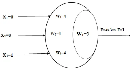
is more sophisticated than the traditional Boolean gates, and TLGs can implement complex logic functions. In a TLG, weights are the principal elements that define the functionality of a gate. A basic TLG consists of N-inputs, a weight value for each input, and a threshold weight. The sum of the input weights is compared with the threshold weight. If it is greater than the threshold weight, then the digital output of TLG is logic high, and if it is less it will be logic zero. In the CMOS-based implementation considered in this paper, when the sum of the input weights is equal to the threshold weight, then the gate is in undefined state. Weights are selected so that this case is avoided. The equation representing the output of a TLG is given as
Fig. 1: Functionality of a TLG for a given weight configuration and input pattern.
We present a new implementation, which we call the dual clock current mode logic (DCCML), which results in both speed and switching energy [power-delay product (PDP)] improvements over the approaches. They consist of two parts: the differential part and the sensor part. All the p-MOS transistors in the sensor part have the same size S, which we call the sensor size. The sensor size impacts the performance of all the three current mode implementations for any threshold logic function. It is a very time-consuming task to obtain the optimum sensor size through iterative SPICE simulations, one simulation for a different sensor size.
An automatic test pattern generation approach to detect delay defects in a circuit consisting of current mode threshold logic gates is introduced. Each generated pattern should excite the maximum propagation delay at the fault site. Manufactured weights may vary, and maximum delay is ensured by applying an appropriately generated set of patterns per fault. Experimental results show the efficiency of the proposed method. As an approach to clarifying the basic properties of threshold logic, the completely monotonic function is investigated. Its testing procedure, functional form, etc., are discussed by using a new concept, mutual monotonicity. If the network contains cycles, however, the computation is not uniquely defined by the interconnection pattern and the temporal dimension must be considered. When the output of a unit is fed back to the same unit, we are dealing with a recursive computation without an explicit halting condition. We must define what we expect from the network: is the fixed point of the recursive evaluation the desired result or one of the intermediate computations? To solve this problem we
assume that every computation takes a certain amount of time at each node (for example a time unit).
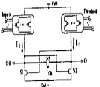
Fig. 2: Current mode TLG
Low-power dissipation is achieved by limiting the voltage swing on the interconnects and the internal nodes of the CMTL gates. High-performance is achieved by the use of transistor configurations that sense a small difference in current and set the differential outputs to the correct values. The realization of NAND, NOR, AND, OR logic gates and other logic functions using the CMTL gates is presented. We also present several implementations of CMTL gates and describe the relative advantages and limitations of these implementations. These computing elements are a generalization of the common logic gates used in conventional computing and, since they operate by comparing their total input with a threshold, this field of research is known as threshold logic.
II. LITERATUR SURVEY
Delay Analysis for Current Mode Threshold Logic Gate Designs.
existing implementations in delay as well as switching energy.
Low power, high speed, charge recycling CMOS threshold logic gate
A new implementation of a threshold gate based on a capacitive input, charge recycling differential sense amplifier latch is presented. Simulation results indicate that the proposed structure has very low power dissipation and high operating speed, as well as robustness under process, temperature and supply voltage variations, and is therefore highly suitable as an element in digital integrated circuit design.
A Low Power, High Performance Threshold Logic-Based Standard Cell Multiplier in 65 nm CMOS
In this paper we describe the design, simulation, fabrication, and test of a 32-bit 2's complement integer multiplier constructed from a combination of CMOS standard cells and threshold logic elements in a 65 nm low power process. As compared to a multiplier designed solely using CMOS standard cells, the threshold logic based multiplier is 1.23x smaller and consumes 1.41x less dynamic power and 2.5x less leakage power at the same process corner.
III. Current-Mode Threshold Logic
Gates(CMTLG).
Fig. 2 shows the a general circuit diagram of the CMTL gates. The low-swing inputs are fed to a PMOS based CMTL gate. The CMTL gate senses the low input swings, performs the logic computations and creates full-swing output voltages. The output nodes of the CMTL gate with full-swing are used as inputs to the nMOS based interconnect driver. In the next section, we describe the current-mode threshold logic gates and present several implementations of threshold logic gates.
A threshold gate is a super-set of logic gates such as AND, NAND, OR, NOR. It can be used to realize more complicated functions such as majority function in a single logic gate. Fig. 3. shows the basic operation of the current-mode threshold logic gate. Since the input voltage swing is between VL and Gnd, the PMOS transistor is used to translate the input voltage into current. When the input at the gate terminal of the PMOS transistor is Gnd it can drive a larger current compared to the PMOS transistor with the a gate input voltage of VL. For small values of VL, the PMOS transistor is always ON.
Fig.3. Basic current-mode threshold logic operation
CMTLG AND DCML IMPLEMENTATIONS OF A THRESHOLD LOGIC FUNCTION
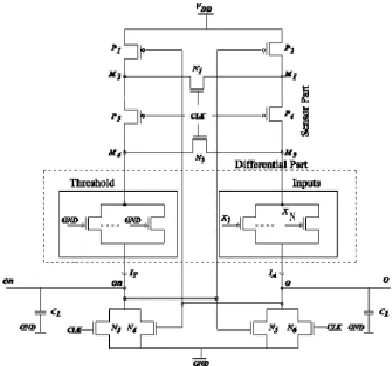
The nodes connecting the differential part and the sensor part on the input side and the threshold side are
M1 and M2,respectively. The sensor part has three
p-MOS transistors P1, P2, P3, and four n-p-MOS transistors N1, N2, N3, and N4 as shown in figure below. If the size of the sensor is S, then all the p-MOS transistors in the sensor part have S μm size and all the n-MOS transistors in the sensor part have a size smaller than S μm. The operation of the CMTLG is divided into two phases: the equalization phase and the evaluation phase.
Fig. 4: Block diagram of differential current mode logic.
An alternative differential clock threshold logic implementation is presented in, and it is referred to as the differential current mode logic (DCML) approach. Its block diagram is shown in Fig. 3.4. It is also divided into the differential part and the sensor part. The currents through the threshold part and the inputs part are also denoted by IT and IA, respectively. The sensor part consists of four p-MOS transistors,labeled P1–P4, and six nMOS transistors, labeled N1–N6. The load capacitance CL is applied to both the output nodes O and OB.
Fig. 5: Output voltages and their difference in the two clock phases for DCML.
The applied clock is divided into two phases: when the clock is high the TLG is in the equalization phase and when it is low it operates on the evaluation phase. In the equalization phase, nMOS transistors N1, N2, N3,
and N6 are active. Transistor N1 equalizes the voltage at nodes M1 and M2. Similarly, transistor N2 equalizes the voltage at nodes M3 and M4.
Demerits of Existing System.
Existing system consist of two parts: the differential part and the sensor part. All the pMOS transistors in the sensor part have the same size S, which we call the sensor size. The sensor size impacts the performance of all the three current mode implementations for any threshold logic function. It is a very time-consuming task to obtain the optimum sensor size for different sensor size, which is the drawback. In the proposed we are reducing the power.
IV. LOW POWER AND HIGH-SPEED
DUAL-CLOCK-BASED CURRENT
In the given weight configuration, we have two positive weights w1andw2 and two negative weights w3 and w4. Weights w1 and w2 are implemented in the positive inputs section and weights w3 and w4 are implemented in the negative inputs section. The threshold weight wT is implemented in the positive threshold section. The current through the four blocks (positive threshold, negative inputs, negative threshold, and positive inputs) are denoted by IPT , IN I , INT , and IP I , respectively. The currents through transistors P5 and P6 are denoted by I 5 P and I 6 P. Here, I 5 P = IPT + IN I and I 6 P = INT + IP I . Nodes OP and OPB are the output nodes. The load capacitance is denoted by CL. The operation is divided into three phases: the equalization phase, the pre-evaluation phase, and the final-evaluation phase. When clocks Clk1 and Clk2 are high, then the circuit is in the equalization phase. When clocks Clk1 and Clk2 are low, then the circuit is in the pre-evaluation phase. It is noted that when the two clocks are not completely aligned the operation of the gate is not effected. The possible cases of misalignment are: 1) the falling edge of Clk2 comes before the falling edge of Clk1 and 2) the falling edge of Clk2 comes after the falling edge of Clk1. In the first case, the current from the differential part is equalized because of transistor N1 and the evaluation phase starts after the falling edge of Clk1. In the second case, there will be no current from the differential part as Clk2 is not active yet. Hence, the pre-evaluation phase starts after the falling edge of Clk2. The implementation avoids a very early arrival of Clk1. In that case, a non- stable signal might result in erroneous output.
two time phases: the activation time and the boosting time. The activation time is the time taken by the circuit to develop an initial voltage difference at the output nodes O P and OPB. The boosting time is the time taken by the DCCML to bring the initial voltage to the correct voltage at the output nodes O P and OPB. In the pre-evaluation phase, both the differential part and the sensor part are active, and therefore the activation time is not affected. In the final evaluation phase, the differential part is kept inactive using Clk2. Therefore, the effect of internal capacitance due to the differential part is isolated. Hence, it takes very little time to boost the outputs to the final value. The power is also reduced due to the isolation of the differential part.
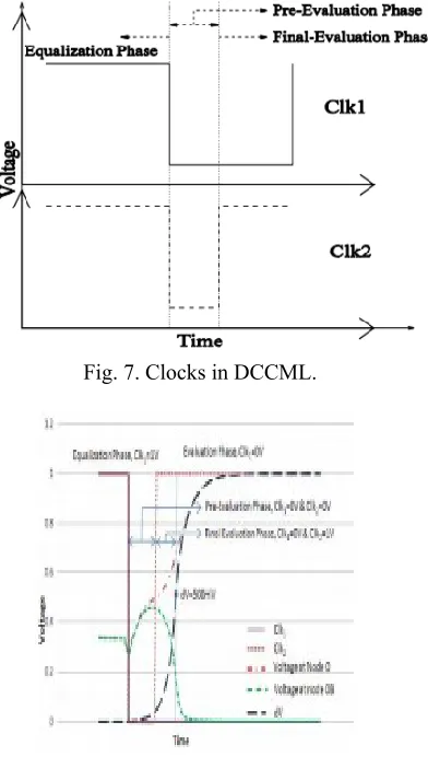
Fig. 7. Clocks in DCCML.
Fig. 8. Voltage at output nodes OP and OPB and dV during the three clock phases.
DELAY MINIMIZATION BY AN APPROPRIATE SENSOR SIZE SELECTION.
This section presents an analytical formula to compute the sensor size that minimizes the gate delay. Let N denote the number of inputs, N the sum of all positive input weights, and T the sum of the threshold weight and negative input weights.
Our analysis assumes that all the input weights are connected in parallel, and that each weight wi can be implemented by wi unit width pMOS transistors connected in parallel. This is an accurate assumption. We have implemented TLG weights using a smaller number of wider pMOS transistors connected in parallel and SPICE simulations showed no difference in the performance of the TLG. This is further explained in the example below.
obtain the worst case delay for logic 1 at the output node O, the current difference IA−IT should be minimum. For logic 0, this current difference should also be minimum. Since transistors on the threshold side are always ON, the maximum delay for a rising transition of the output is obtained when we have T +1 active transistors. Likewise, T −1 active transistors tend to obtain the worst case delay for a falling transition at the output. However, it is known that the worst case delay occurs for rising output transition [1]. Hence, a worst case delay pattern is one that gives the least current difference at nodes M1 and M2. The following is an example where SPICE simulations confirm this analysis.
Fig. 9. CMTLG delay with N = 11 and T = 4 as NA varies.
V. RESULT Current mode TLG.
Schematic.
Layout.
Simulation.
Block diagram of differential current mode logic. Schematic.
Layout.
Schematic of DCCML TLG.
Layout.
Simulation.
Comparison Table.
SYSTEM POWER
EXISTING
(CMTLG) 0.256𝑚𝑊
PROPOSED
(DCCML TLG) 1.555
𝜇𝑊
V. CONCLUSION
An analytical method has been proposed to identify quickly the transistor size in the sensor component of a current mode implementation that ensures very low gate delay (very close to the minimum), independent of the current mode method used to implement the threshold logic function. A new current mode implementation method was also proposed that outperforms existing implementations both in gate delay as well as energy.
Future Scope.
In current-mode logic (CML), logic levels are represented by current levels. It has several advantages
over voltage-mode logic (VML). New Ternary
minimum (Logical AND) and maximum (Logical OR) circuits can be done in the future, that are based on CNTFET technology and CML design technique which reduces both area and power.
REFERENCES
[1] S. Bobba and I. N. Hajj, ―Current-mode threshold logic gates,‖ in Proc. IEEE ICCD, Sep. 2000, pp. 235– 240.
[2] T. Ogawa, T. Hirose, T. Asai, and Y. Amemiya, ―Threshold-logic devices consisting of subthreshold CMOS circuits,‖ IEICE Trans. Fundam. Electron., Commun. Comput. Sci., vol. E92-A, no. 2, pp. 436– 442, 2009.
[3] S. Muroga, Threshold Logic and Its Applications. New York, NY, USA: Wiley, 1971.
high performance threshold logic-based standard cell multiplier in 65 nm CMOS,‖ in Proc. IEEE Comput. Soc. Annu. Symp. VLSI, Lixouri, Greece, Jul. 2010, pp. 210–215.
[6] M. Sharad, D. Fan, and K. Roy. (2013). ―Ultra-low energy, highperformance dynamic resistive threshold
logic.‖ [Online]. Available:
http://arxiv.org/abs/1308.4672
[7] P. Celinski, J. F. López, S. Al-Sarawi, and D. Abbott, ―Low power, high speed, charge recycling CMOS threshold logic gate,‖ Electron. Lett., vol. 37, no. 17, pp. 1067–1069, Aug. 2001.
[8] S. Leshner and S. Vrudhula, ―Threshold logic element having low leakage power and high performance,‖ WO Patent 2009 102 948, Aug. 20, 2009.
[9] T. Shibata and T. Ohmi, ―A functional MOS transistor featuring gatelevel weighted sum and threshold operations,‖ IEEE Trans. Electron Devices, vol. 39, no. 6, pp. 1444–1455, Jun. 1992. [10] V. Beiu, J. M. Quintana, and M. J. Avedillo, ―VLSI implementations of threshold logic—A comprehensive survey,‖ IEEE Trans. Neural Netw., vol. 14, no. 5, pp. 1217–1243, Sep. 2003. [11] T. Gowda, S. Leshner, S. Vrudhula, and S. Kim, ―Threshold logic gene regulatory networks,‖ in Proc. IEEE Int. Workshop GENSIPS, Jun. 2007, pp. 1–4.
[12] A. K. Palaniswamy and S. Tragoudas, ―A scalable threshold logic synthesis method using ZBDDs,‖ in Proc. 22nd Great Lakes Symp. VLSI, 2012, pp. 307– 310.
[13] C. B. Dara, T. Haniotakis, and S. Tragoudas, ―Delay analysis for an N-input current mode threshold logic gate,‖ in Proc. IEEE Comput. Soc. Annu. Symp. VLSI (ISVLSI), Aug. 2012, pp. 344–349.