DESIGN OF RECONFIGURABLE MULTIPLE
ELEMENTS MICROSTRIP RECTANGULAR LINEAR ARRAY ANTENNA
M. T. Ali, M. R. Kamarudin, and T. A. Rahman
Wireless Communication Center (WCC) Universiti Teknologi Malaysia
81310 UTM Skudai, Johor, Malaysia
R. Sauleau
Institut d’´electronique et de t´el´ecommunications de Rennes i, (IETR) UMR CNRS 6164, University of Rennes 1, France
M. N. Md Tan
Wireless Communication Center (WCC) Universiti Teknologi Malaysia
81310 UTM Skudai, Johor, Malaysia
Abstract—This paper presents a reconfigurable multiple element microstrip rectangular linear array antenna integrated with radio frequency (RF) switches. The corporate feed design concept is used to excite the linear array antenna that consists of 8 elements of rectangular patches at 5.8 GHz. Two PIN diode switches were deployed at the feeding line to activate the two arrays of patches that are located on the left and right sides of the antenna structure. The behavior of the reconfigurable multiple element linear antenna array system has been investigated with respect to the beam shaping characteristic. The comparisons of the performance between two structures, with and without Wilkinson Power Divider (WPD) are discussed in this paper. Two different beam patterns were achieved through the reconfigurable antenna at different number of elements design that incorporates with PIN diode switches and modified WPD concept. The simulation and the measurement results for 4 and 8 elements array antenna structure are presented.
1. INTRODUCTION
The reconfigurable antennas have drawn lots of attention in the wireless communication systems recently. The demand for reconfigurable antenna has increased drastically since a decade. Reconfigurable beam shaping is an ideal for the detection of small and large targets at both short and long ranges, including that the antenna is mounted on a high tower or hillside [1, 2]. Reconfigurable antennas are ideal for many military and mobile communication applications where it is required to have a single antenna that can be dynamically reconfigured to transmit or receive on the same or multiple frequency bands [3– 5]. It is advantageous to integrate beam shaping functionality into the systems so one can vigorously vary the beam shapes in many applications such as airplane radar, protection from smart weapons and point to point communication.
In [6, 7], the authors presented reconfigurable antennas, which radiated at different beam pattern by adjusting the apertures and maintaining their operating frequencies. The antenna presented in [3], described a dual band dipole antenna integrated with MEMS switches. However, this method typically used a dual operating frequency to reconfigure the beam pattern. The antennas proposed in [8, 9] worked at dual operating frequencies with a reconfigurable radiation pattern. In the reconfigurable antenna, the structure of the antenna can be changed by integrating with the switches such as PIN diode switches [10], the field-effect transistor (FET) [11], the photo conductor switches [12] or by electromechanical system (MEMS) switch [13–15], which were proposed a few years ago. By controlling the states of the switches, to ON or OFF mode, several approaches were proposed for implementing the reconfigurable antenna. Most of these approaches were able to alter the fundamental characteristics of the antenna such as operating frequency, bandwidth, polarization characteristics and radiation pattern [13].
2. ANTENNA DESIGN
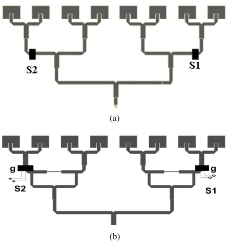
The configuration of the proposed reconfigurable antenna structures is shown in Figure 4. There are two structures of reconfigurable microstrip patch antenna proposed in this design, without WPD as in structure 1 and added with modified WPD as in structure 2. The antenna structure was constructed on FR-4 glass epoxy substrate which has a relative permittivity (εr) of 4.6 and loss tangent (δ) of 0.03; the thickness of the substrate is 1.6 mm.
(a) (b)
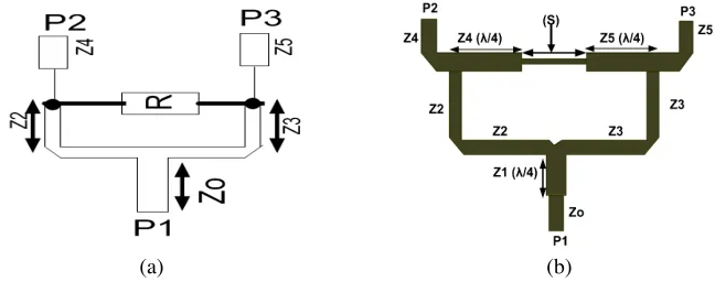
Figure1. (a) Conventional Wilkinson power divider (b) the modified Wilkinson power divider geometry.
2.1. Power Divider Concept
The power divider is one of the most commonly used components in RF and microwave systems for power division and/or combination ratio as n-port network. The ideal design parameters are given in [8]. There are two common types of power divider used in an array antenna design, which are Wilkinson power divider and T-junction power divider. Figure 1 shows the structure of Wilkinson power divider. A lumped resistor, 100 Ω (R), is connected between the outputs of two branches and provides the required isolation. The dimensions of chip resistor must be very small, of the order of 1×0.5 mm. This implies that the two branches of the power divider must be placed very close to each other to be connected to the resistor. This could produce strong mutual coupling between the output lines.
To overcome this problem, the 100 Ω chip resistor will be replaced by theλ/4 lengths of 100 Ω transmission line (S). Aλ/4 length of 100 Ω transmission line is placed in betweenλ/4 length of 50 Ω transmission line (Z4 and Z5) as in Figure 1(b). The electrical performance of the WPD depends on the length of transmission line. These properties of modified WPD are illustrated in Table 1. In Figure 2, it can be seen that when the length of 100 Ω transmission line increases, the resonant frequency of the divider is shifted to the higher frequency, and the matching performance becomes worse. For these reasons, the proposed modified WPD is designed using 100 Ω transmission line with a length of 0.209λg. Figure 3 shows the performance of modified WPD which has good electrical characteristic with−39 dB of return loss at 5.8 GHz.
Table1. The properties of modified Wilkinson power divider.
Characteristics Z0 Z1 Z2 Z3 Z4 Z5
Impedance (Ω) 50 42.04 59.46 59.46 50 50 Width (W), mm 2.92 3.65 2.239 2.239 2.92 2.92
A Wilkinson power divider with an arbitrary power ratio is expressed as follows in Equation (1) to (7) [17].
P2
P3
= 1
K2 (1)
Z2 = Z0
K(1 +K2) (2)
Z3 = Z0
(1 +K2)
Figure3. Return loss plot for modified WPD.
(a)
(b)
(a)
(b)
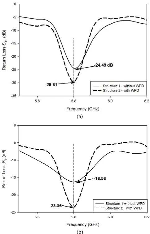
Figure5. Comparison of return loss S11 (dB) between antenna
structures 1 and 2 (a) 4 radiated elements (b) 8 radiated elements.
Z4 = Z0
√
K (4)
Z5 =
Z0
√
K (5)
R = Z0 =
1 +K2
K (6)
w = exp
zc √
εr+ 1.41
87
0.8
(b) (a)
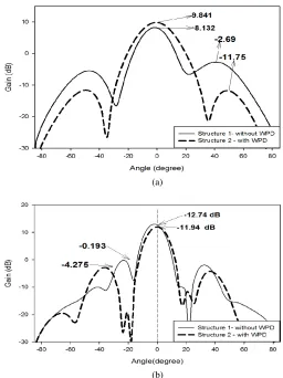
Figure6. Comparison of radiation pattern between antenna structure 1 and 2 (a) 4 radiated elements (b) 8 radiated elements.
where: w= width of transmission line H= thickness of substrate εr= dielectric constant
2.2. Corporate Feed Patch Array Structure
Table2. The summary of simulation results obtained for the reconfigurable linear array antenna for both structures.
Antenna Return loss S11(dB) Gain (dB) Sidelobe Ratio (dB)
ON OFF ON OFF ON OFF
Structure 1 −16.56 −24.49 12.74 8.13 12.93 10.82
Structure 2 −23.56 −29.61 11.94 9.84 16.22 21.6
Figure7. Schematic representation of the switching circuit components inserted in active feeding network.
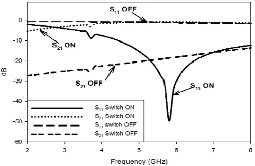
Figure8. Calculated return loss (S11) for ON and OFF states (a)
switch ON mode and (b) switch OFF mode.
Figure9. Photo of the fabricated reconfigurable linear array antenna with single stub matching and PIN diodes.
at the same frequency.
(b) (a)
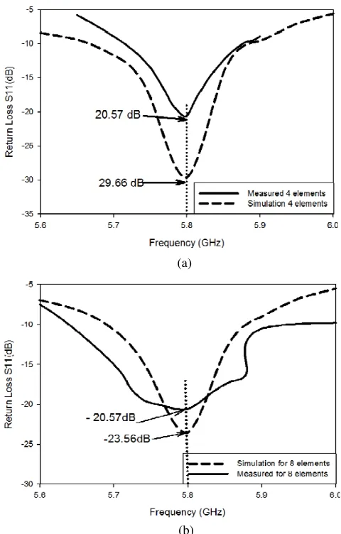
Figure10. Measured and simulation results of return loss S11(dB) for
structure 2 (a) 4 elements radiated (b) 8 elements radiated structure.
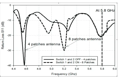
Figure11. Measured results of S11 when switch on/off state.
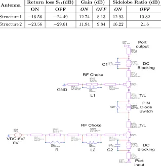
2.3. PIN DiodeRF Switching Circuit
Philips PIN diodes, BAP51-02 [16] have been selected in this design. Figure 7 shows the schematic diagram of the switching circuit. It can be seen that the switch is inserted in between two transmission lines. Each switching circuit consists of a PIN diode, two DC block capacitors, two inductors and one resistor. The capacitors, (C1-C2), are used as DC blocking and the inductors, (L1-L2), are used as RF chokes which provide low impedance for DC. The biasing voltage (6 V) has been connected to 100 Ω resistor to limit the current flow to the switch. The simulation results using the PIN diode’s equivalent circuits for the OFF and ON-stages are presented in Figure 8. The return loss is less than −40 dB for the ON stage and an approximate of 0 dB for the OFF stage at 5.8 GHz. The selected capacitance and inductance values were chosen to be 6.8 pF and 22 nH, respectively.
3. EXPERIMENTAL RESULT
(b) (a)
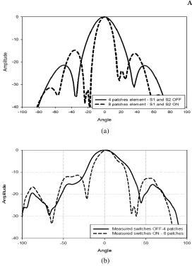
Figure12. Simulation and measured results of normalized radiation pattern for 4 and 8 element structures.
The radiation pattern of the 4 and 8 elements structure are shown in Figure 12(a) with 3 dB half power beamwidth (HPBW) of 22◦ and 12.6◦, respectively. Meanwhile the simulated return loss for the two structure are −29.43 dB and −23.56 dB, respectively as shown in Figure 10. Referring to Figure 12, it is clearly shown that when the numbers of the elements are increased, the beamwidth becomes narrow with lower sidelobe and higher magnitude.
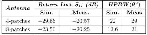
Table3. Selectable performance for the reconfigurable microstrip antenna for structure 2.
Antenna Return Loss S11 (dB) HPBW(θ
◦)
Sim. Meas. Sim. Meas
4-patches −29.66 −20.57 22 29 8-patches −23.56 −20.25 12.6 21
results for both types of configurations (4 and 8-elements) are shown in Figure 10. The antenna shows good impedance matching for both cases with better than 20 dB return loss observed. Figure 11 shows the measurement of return loss when the switches are turned to ON and OFF-stages. The measured radiation patterns, in Figure 12(b), show very good agreement with the simulation. The results show two different beam patterns at −3 dB, about 29◦ and 21◦ at the same frequency. Table 3 is the summary of simulation and measurement results obtained for the reconfigurable linear array antenna.
4. CONCLUSION
In this paper, experimental data have demonstrated the concepts of reconfigurable number of elements that produced broad and narrow beam radiating pattern characteristics. By using a modified WPD in the antenna structure, it produced a better performance in terms of return loss. This research has taken advantage of the flexibility of the number of elements technique by applying it to the problem of reconfigurable multiple beam array combination. The reconfigurable dual-beam antenna pattern at fixed frequencies across the entire 5.7– 5.9 GHz band is presented in this paper with excellent radiation patterns.
REFERENCES
1. Chang, C. C., C. Liang, B. H. Deng, C. W. Domier, and N. C. Luhmann, Jr., “A beam-shaping phased antenna array based on true-time delay technologies,”Infrared and Millimeter Waves, 99–100, 2002.
3. Kiriazi, J., H. Ghali, H. Ragaie, and H. Haddara, “Reconfigurable dual-band dipole antenna on silicon using series MEMS switches,”
Antennas and Propagation Society International Symposium,
Vol. 1, 403–406, 2003.
4. Mak, A. C. K., C. R. Rowell, R. D. Murch, and C. L. Mak, “Re-configurable multiband antenna designs for wireless communica-tion devices,” IEEE Transactions on Antennas and Propagation, 1919–1928, Vol. 55, 2007.
5. Christodoulou, C. G., D. Anagnostou, and V. Zachou, “Lead invited talk: Reconfigurable multifunctional antennas,” IEEE, 176–179, 2006.
6. Simons, R. N., “Novel on-wafer radiation pattern measurement technique for MEMS actuator based reconfigurable patch antennas,”Technical Report, 24th Annual Antenna Measurement
Techniques Association Meeting and Symposium, NASA/TM—
2002-211816 NASA, Glenn Research Center, Cleveland, Ohio, 2002.
7. Pringle, L. N., P. G. Friederich, S. P. Blalock, G. N. Kiesel, P. H. Harms, D. R. Denison, E. J. Kuster, T. L. Fountain, and G. S. Smith, “GTRI reconfigurable aperture design,” IEEE Transactions on Antennas and Propagation, Vol. 1, 473–476, 2002. 8. Yang, F., X.-X. Zhang, X. Ye, and Y. Rahmat-Samii, “Wide-band E-shaped patch antennas for wireless communications,” IEEE Transactions on Antennas and Propagation, Vol. 49, 1094–1100, 2001.
9. Peroulis, D., K. Sarabandi, and L. P. B. Katehi, “Design of reconfigurable slot antennas,” IEEE Transactions on Antennas and Propagation, Vol. 53, 645–654, 2005.
10. Medeiros, C., A. Castela, J. Costa, and C. Fernandes, “Evaluation of modelling accuracy of reconfigurable patch antennas,”ConfTele, Vol. 1, 13–16, Peniche, Portugal, May 2007. 11. Pringle, L. N., P. H. Harms, S. P. Blalock, G. N. Kiesel, E. J. Kuster, P. G. Friederich, R. J. Prado, J. M. Morris, and G. S. Smith, “A reconfigurable aperture antenna based on switched links between electrically small metallic patches,”IEEE Transactions on Antennas and Propagation, Vol. 52, 1434–1445, 2004.
12. Panagamuwa, C. J., A. Chauraya, and J. C. Vardaxoglou, “Fre-quency and beam reconfigurable antenna using photoconduct-ing switches,”IEEE Transactions on Antennas and Propagation, Vol. 54, 449–454, 2006.
F. De Flaviis, “Multifunctional reconfigurable MEMS integrated antennas for adaptive MIMO systems,” IEEE Communications Magazine, Vol. 24, 62–70, 2004.
14. Weedon, W. H., W. J. Payne, and G. M. Rebeiz, “MEMS-switched reconfigurable antennas,” IEEE Antennas and Propagation Int. Symp., 654–657, Salt Lake City, UT, July 2001.
15. Zendejas, J. M., J. P. Gianvittorio, Y. Rahmat-Samii, and J. W. Judy, “Magnetic MEMS reconfigurable frequency-selective surfaces,” Journal of Microelectromechanical Systems, Vol. 15, 613–623, 2006.
16. “BAP51-02General Purpose PIN Diode, Phillips Technologies Data Sheet, 2006.
17. James, J. R. and P. S. Hall, “Handbook of Microstrip Antennas, Vol. 2, Peter Peregrinus Ltd., London, United Kingdom, 1989. 18. Lee, K. F. and W. Chen, Advanced in Microstrip and Printed