Frequency Reconfigurable Pixel Antenna with PIN Diodes
Raji George1, *, C. R. S. Kumar1, Shashikala Gangal2, and Makarand Joshi3
Abstract—In this paper a frequency reconfigurable pixel antenna is implemented using PIN diodes. The overall dimension of the patch antenna is 26.9×24.5 mm, and it is fabricated on an FR4 substrate. The design is investigated by the simulation and measurement ofS11parameters and radiation patterns. With different combinations of PIN diode biasing conditions, the antenna can be set to 2.5 GHz, 3.9 GHz, and 10 GHz. The antenna shows a consistent radiation pattern at all the reconfigured frequency bands. In the accessible frequency range, an average gain of 6 dB and low level of cross polarization are also recorded. A good agreement between the measured and simulated results validates the presented concept of frequency reconfiguration.
1. INTRODUCTION
Pixel antennas are one of the most promising antenna architectures for the next generation of reconfigurable antenna due to their high level of reconfigurability, covering wide frequency ranges, steering the beam over large angular ranges, and switching between multiple polarizations. A reconfigurable pixel patch antenna consists of a grid of electrically small metallic patches where each pair of adjacent patches is interconnected by RF switch [1–5].
The activation or de-activation of these switches modifies the current distribution over the antenna surface therefore providing reconfiguration capability to the antenna structure. This structure reshaping capability is what allows pixel antennas to achieve a high degree of reconfigurability over frequency, radiation pattern, and polarization. Pixel antenna can have different shapes by switching in and out of the antenna aperture in response to the required operating condition. Pixel reconfigurable antennas are being used in applications like cognitive radio, mobile communication, navigational aircrafts, satellite communication, wireless communication, and software defined radio.
In this paper, the pixel antenna architecture consists of rectangular metallic pixels interconnected by PIN diode switches on an FR4 substrate [6]. The antenna is excited through a coaxial probe formed by extending the inner conductor of the coaxial line to the patch and connecting the external side of the coax to the ground plane in the back of the substrate. PIN diodes are used for the reconfigurability. A pin diode is a semiconductor device that exhibits nonlinear behaviour. The diode can be made to behave as either short circuit or an open circuit depending on the biasing DC voltage across its terminals. This behaviour has been exploited in the design of RF switches. PIN diode switches are inexpensive devices with the maximum dimension of a few millimetres. They have fast switching times, but since they draw current in the ON state they have a relatively high DC power consumption. PIN diodes have been integrated into various antennas structures in order to implement the discrete frequency tuning. Examples include printed dipoles, slot antennas, microstrip patch antennas, and dielectric resonator antennas.
Reconfigurability can be achieved in many radiators by deforming the physical shape or altering the antenna dimensions. In this type of resonant type antenna, a change in one or more dimensions shifts the resonant frequency.
Received 18 May 2019, Accepted 19 July 2019, Scheduled 7 August 2019
Fast switching speed, low operating voltage and edge of integration are the factors which make PIN diode more suitable than other RF switches like FETs and MEMS switches. The objective is to demonstrate a method of frequency reconfiguration with stable radiation characteristics. Antenna size, simplicity of the design, power consumption of the reconfiguring circuitry are also taken into consideration. The proposed antenna is a single band antenna with the ability of frequency hopping. Due to the dependence of the resonance frequency of an antenna on the length of the current path, this elongation results in lowering of frequency from the originally designed value. The proposed reconfigurable antenna uses PIN diodes as switching elements for shorting pins.
2. PIXEL PATCH ANTENNA
Pixels are sub-wavelength metallic patches which, when being interconnected, produce reconfigurability of the radiation properties of the antenna. Conventionally, the pixel shape is taken as a square, but any geometrical shape of the pixel can be chosen such that replicating the basic shape should produce a plane tessellation. The second essential component in pixel antennas is an RF switch interconnecting the adjacent pixels. The isolation of the switches should be over 12 to 14 dB. This has adequate effect on antenna efficiency.
3. DESIGN GUIDELINES
The pixel patch antenna is designed to provide the required reconfiguration capability. Fig. 1 shows the schematic of the Pixel Antenna with switches. The total size Lt of the pixel surface is determined by the required gain of the pixel antenna which gives the lowest frequency. The resulting value is the lower bound for the antenna size, and the actual size should be larger to account for the efficiency of the pixel aperture and the losses produced by the switches.
Figure 1. Pixel antenna with RF switches.
While the total size has to be large enough to meet the radiation pattern and frequency requirements, the individual pixel size is small enough to tune the highest frequency required.
Since the minimum total size (Lt) of the pixel antenna is half a wavelength (for the lowest frequency) as given by Eq. (1), and the maximum individual pixel size (Lp) is a sixth of a wavelength as given by Eq. (2), it can be directly concluded that pixel antenna requires 3×3 pixels [7, 8]
Lt> λlow/(2√εreff) (1)
Lp < λup/(6√εreff) (2)
where λlow is the wavelength for lowest frequency possible, and λup is the wavelength for highest frequency possible.
Applying Eqs. (1)–(2), the dimensions of the pixel antenna are Lt = 24.5 mm for the lowest frequency of 2.5 GHz andLp = 6.5 mm for the highest frequency of 10 GHz.
4. RF SWITCHES
Semiconductor switches, such as PIN diodes and FET transistors, are the main switching components used by pixel antennas. They have fast switching times, low cost, excellent reliability, and compatibility with standard PCB assembly processes. Their insertion loss and isolation levels are acceptable at frequencies up to a few Gigahertz, and their power consumption is in general compatible with wireless communication devices. The characterization of the switch is an important step to validate its good performance over the frequency range of operation and to ensure the accuracy of the pixel antenna simulations.
5. PIN DIODE AS AN RF SWITCH
At RF frequencies, the PIN diode behaves as a variable resistor with the following circuit models as shown in Fig. 2. Both On and OFF states have a package inductanceL. Fig. 2 shows the equivalent circuits for the PIN diode in ON and OFF states. The equivalent circuit in the ON state (forward biased) has a low resistanceRs which contributes to the insertion loss. The equivalent circuit for OFF state (zero or reverse biased) has the parallel combination of the reverse bias resistance Rp and the total capacitance C which contributes to isolation.
6. PIN DIODE SMP1340-079
The semiconductor switch corresponds to the model SMP1340-079 from Skyworks Solution Inc. [9]. SMP 1340-079 is used in fast speed wireless switch applications. The SMP1340 series of plastic packaged, surface mountable PIN diodes is designed for high volume switch applications from 10 MHz to more than 10 GHz. The short carrier lifetime of 100 ns (typical), combined with their thin I-region width of 5µm (nominal), results in a group of fast speed RF switching PIN diodes. The RF performance of the SMP1340 series as per the data sheet has a low capacitance (0.21 pF @ 5 V) and low resistance (0.85 Ω at 10 mA). SMP 1340-079 has a power dissipation of 250 mW.
7. BIASING OF PIN DIODES
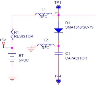
It is necessary to provide some degree of isolation between the low frequency DC bias circuit and the RF circuit. Fig. 3 shows the biasing circuit for a PIN diode. An RF choke inductor is used in series with the bias line, and RF bypass capacitors are connected in shunt with the power supply to keep the DC out of the RF portion of the circuit. This provides 20 dB or more of DC/RF isolation.
The biasing network consists of two capacitors of 0.12 pF as DC blocks, two inductors of 1µH as RF isolators, and the circuit is connected to regulated supply of 5 V.
(a) (b)
Figure 2. Equivalent circuits for PIN diode. (a) ON state. (b) OFF state.
8. SIMULATION
The PIN diodes connected between the adjacent pixels are simulated as lumped RLC parameter in HFSS. Fig. 4 shows the model of pixel antenna with PIN diodes in HFSS. When a PIN diode is ON, the RLC lumped parameters are assigned with the values of Rs = 0.85 Ω and L = 0.7 nH, and when PIN diode is OFF, the RLC parameters are L= 0.7 nH,R = 2kΩ, and C= 0.21 pF. Fig. 4 shows the simulation model of the pixel antenna with the PIN diodes.
Figure 4. Pixel antenna with PIN diodes in HFSS.
The PIN diodes are biased by applying a voltage of 5 V. By controlling the biasing of the PIN diodes, the antenna is made reconfigurable. Different configurations of the pixel antennas are as follows:
(i) Configuration 1: When none of the PIN diodes are biased, only a single row of pixels radiate with the highest frequency possible.
(ii) Configuration 2: When only one row of PIN diodes (P4, P5, P6) are biased and turned ON, the antenna aperture reduces to 2×3 pixel antenna with only 2 rows of 3 pixels radiating. The radiating frequency is the intermediate frequency.
(iii) Configuration 3: When all PIN diodes (P1–P6) are turned ON by biasing, the antenna aperture is of 3×3 pixels with all the pixels radiating. The radiating frequency is the least frequency possible with this pixel antenna.
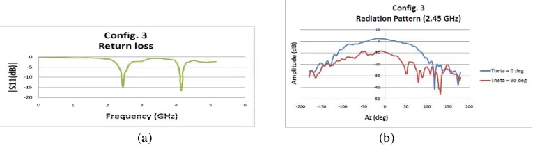
The simulation results are as shown in Figs. 5(a)–(b). S11 parameters are plotted for all the three configurations as shown in Fig. 5(a) by providing biasing voltage to the PIN diodes.
The radiation patterns are plotted as shown in Fig. 5(b). Fig. 5(b) shows the radiation pattern with a gain of 4.26 dB for Configuration 1, 3.52 dB for Configuration 2, and 4.35 dB for Configuration 3.
9. FABRICATION
The pixel antenna is fabricated on an FR4 substrate with the bias circuit of PIN diodes. The layout circuit for the pixel antenna structure is as shown in Fig. 6.
Bias voltage of +5 V is provided asV1 and V2. This bias voltage biases the PIN diodes.
Configuration 1 is obtained whenV1 = 0 V andV2 = 0 V; Configuration 2 is obtained whenV1 = 0 V and V2 = 5 V; and Configuration 3 is obtained whenV1 = 5 V andV2 = 5 V. In Configuration 1, all the PIN diodes are OFF; in Configuration 2, PIN diodes P4, P5, and P6 are turned ON; and in Configuration 3, all the PIN diodes are turned ON.
(iii) Config. 3
(i) Config. 1 (ii) Config.2
(a)
(b)
Figure 5. (a)S11 parameter for the different configurations: Config. 1 when all PIN diodes are OFF; Config. 2 When PIN diodes P4, P5, P6 ON; Config. 3 When all PIN diodes ON. (b) Radiation pattern for all the three configurations.
Figure 6. Pixel antenna with PIN diodes and bias circuit.
S11 parameter is measured on VNA Rohde and Schwarz ZVA 40 for all three configurations by biasing the PIN diodes with a voltage of 5 V. The measurement results are shown as Figs. 8(a), 9(a), and 10(a) for the three configurations.
The radiation patterns of the three configurations are measured in an anechoic chamber. Figs. 8(b), 9(b), and 10(b) show the radiation patterns for all the three configurations.
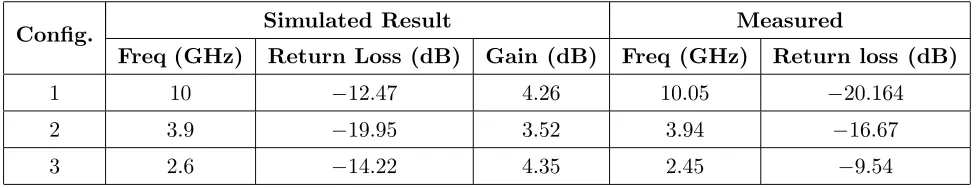
The simulated and measured results are tabulated in Table 1. From Table 1 it is observed that the simulated result is in good agreement with the measured one. It is observed that there is a slight variation in the results. This deviation is attributed to the losses due to the PIN diodes and the biasing circuit components for the PIN diodes.
(a) (b)
Figure 8. Measurement results of Configuration 1: when all PIN diodes are OFF. (a) S11 parameter for config. 1 when V1 = 0 V and V2 = 0 V. (b) Radiation pattern for Config. 1 for theta = 0 deg and 90 deg.
(a) (b)
Figure 9. Measurement results of Configuration 2: When one row of PIN diodes (P4, P5 and P6) are ON. (a) S11 parameter for Config. 2 whenV1 = 0 V andV2 = 5 V. (b) Radiation pattern for Config. 2 for theta = 0 deg and 90 deg.
(a) (b)
Table 1. Summary of the simulated and measured results.
Config. Simulated Result Measured
Freq (GHz) Return Loss (dB) Gain (dB) Freq (GHz) Return loss (dB)
1 10 −12.47 4.26 10.05 −20.164
2 3.9 −19.95 3.52 3.94 −16.67
3 2.6 −14.22 4.35 2.45 −9.54
10. CONCLUSION
A frequency reconfigurable pixel antenna with PIN diodes is designed and fabricated. It is observed that the measured results are in good agreement with the simulated ones. The proposed design has stable radiation characteristics and frequency reconfigurability, and performances are found satisfactory. The work provides a simple and efficient way to realize multiple closely spaced frequency bands into a limited space.
ACKNOWLEDGMENT
The authors are grateful to ARDE, Pune for providing the VNA and Anechoic Chamber facilities for the antenna characterization.
REFERENCES
1. Rodrigo, D., J. Romeu, B. A. Cetiner, and L. Jofre, “Pixel reconfigurable antennas: Towards low-complexity full reconfiguration,” EuCAP 2016, 1–5, 2016.
2. Besoli, A. G. and F. De Flaviis, “A multifunctional reconfigurable pixelled antenna using MEMS technology on printed circuit board,” IEEE Transactions on Antennas and Propagation, Vol. 59, No. 12, 4413–4424, Dec. 2011.
3. Zammit, J. A. and A. Muscat, “Rapid analysis of a pixel patch antenna using the planar circuit technique,” Loughborough Antennas & Propagation Conference, Loughborough, UK, Nov. 14–15, 2011.
4. Yuan, X., Z. Li, D. Rodrigo, H. S. Mopidevi, and O. Kaynar, “A parasitic layer-based reconfigurable antenna design by multi-objective optimization,”IEEE Transactions on Antennas and Propagation, Vol. 60, No. 6, 2690–2701, Jun. 2012.
5. Li, Y.-L., W. Shao, J.-T. Wang, and H. Chen, “An improved NSGA-II and its application for reconfigurable pixel antenna design,”Radio Engineering, Vol. 23, No. 2, 733–738, Jun. 2014. 6. George, R., C. R. S. Kumar, and S. A. Gangal, “Design of a frequency reconfigurable pixel patch
antenna for cognitive radio applications,”International Conference on Communication and Signal
Processig, 1684-16, 2016.
7. Pozar, D. M. and D. H. Schaubert,Microstrip Antenna Design, IEEE Press, Piscataway, NJ, 1995. 8. Balanis, C. A., Antenna Theory: Analysis and Design, John Wiley & Sons, Canada, 2005.