ISSN(Online): 2320-9801 ISSN (Print) : 2320-9798
I
nternational
J
ournal of
I
nnovative
R
esearch in
C
omputer
and
C
ommunication
E
ngineering
(An ISO 3297: 2007 Certified Organization)
Vol. 4, Issue 10, October 2016
Design and Implementation of Scalable Micro
Programmed Fir Filter Using Wallace Tree
and Birecoder
J.Hannah Janet1, Jeena Thankachan2
Student (M.E -VLSI Design), Dept. of ECE, KVCET, Anna University, Tamil Nadu, India1
Assistant Professor, Dept. of ECE, KVCET, Anna University, Tamil Nadu, India2
ABSTRACT: Finite impulse response (FIR) filter is one of the important components in any DSP and communication systems. The output from the DSP processor is depends on the FIR filter, so need an efficient FIR filter design, to achieve an efficient output. Filter architecture contains many components; one of the main components is multiplier. Different types of multipliers are available in the digital circuits, but need an efficient multiplier design to get efficient filters. In the existing Wallace tree multiplier was designed and implemented using verilog HDL. This multiplier needs many gates to implement the design. So it takes more area and delay. To reduce the drawbacks in the existing system, to propose a new efficient multiplier named as Birecoder multiplier. It is one of the best multiplier in the digital circuit design. This multiplier overcomes the existing multiplier drawbacks. Multiplier is design by verilog HDL, after the design Wallace tree multiplier is compared with Birecoder, and analyzes the performance of the multiplier. Implement the design using Modelsim 6.3c and Xilinx ISE. Finally the designed multipliers are applied into the FIR filter, and show the best filte
KEYWORDS: Wallace tree, Birecoder, Modelsim 6.3c, Xilinx ISE, FIR filter.
I. INTRODUCTION
The unstable growth in portable multimedia and mobile computing applications has enlarged the demand for low power digital signal processing (DSP) systems and Wireless Communication. One of the most extensively used functions executed in DSP is Finite Impulse Response (FIR) filtering. In several applications, in order to attain high spectral suppression and noise reduction, FIR filters with moderately huge number of taps are essential. A lot of prior efforts for decreasing power consumption of FIR filter usually focus on the miniaturization of the filter coefficients whereas maintaining a fixed filter order[1& 2] . FIR filter structures are simplified to minimizing the number of additions/subtractions and add & shift operations. Though, one of the problems encountered is that one time the filter architecture is determined, the coefficients cannot be altered consequently, those are not appropriate to FIR filter with programmable coefficients. Fairly accurate signal processing systems are also used for the design of low power digital filters. In FIR filter order vigorously varies along with the stop band energy of the input signal. But the approach affects from slow filter-order adaptation time because of energy calculations in the feedback method [3& 4].
II. DIGITAL FILTERS
ISSN(Online): 2320-9801 ISSN (Print) : 2320-9798
I
nternational
J
ournal of
I
nnovative
R
esearch in
C
omputer
and
C
ommunication
E
ngineering
(An ISO 3297: 2007 Certified Organization)
Vol. 4, Issue 10, October 2016
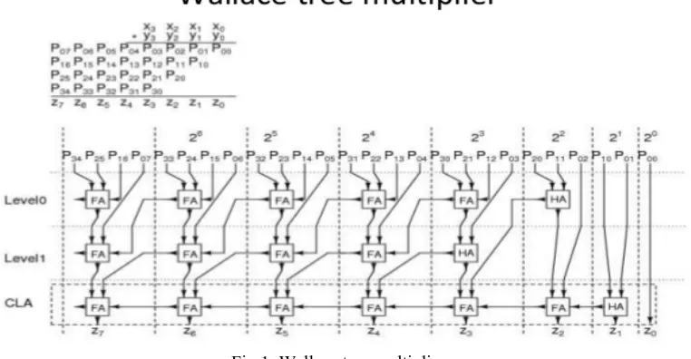
III. EXISTING WALLACE TREE MULTIPLIER
A method for fast multiplication was originally proposed by Wallace tree is an efficient hardware implementation of a digital circuit that multiplies two integers. Using this method, a three step process is employed to multiply two integer numbers. The first step is to multiply each bit of one of the arguments, by each bit of the other, yielding n2 resulst[6]. Based on the position of the multiplied bits, the wires carry different weights. The second step is to reduce the number of partial products to two by layers of full and half adders. The third step is to group the wires in two and then add them using conventional adder . In this paper, two different architectures of Wallace tree multiplier are presented. First one is designed using only half adder and full adder, while the second one uses a more sophisticated carry skip adder (CSA)[7].
Fig 1. Wallace tree multiplier
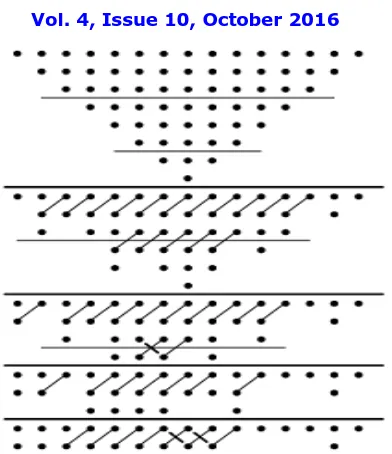
A, STRUCTURE OF REDUCED COMPLEXITY WALLACE MULTIPLIER
A Wallace multiplier is a parallel multiplier which performs the array multiplication effectively [7]. Array multiplier has more number of gates to perform multiplication. Hence, it occupies large area for computation. In order to overcome this problem, Wallace multiplier with proposed SQRT CSLA is designed. Fig 3 shows reduced complexity Wallace multiplier structure. The reduced complexity Wallace multiplier consists of reduced number of half adders when compared to the conventional Wallace multiplier [8]. In the modified circuit, N2 AND gates form the partial products and they are arranged in an inverted triangle order. The matrix is divided into three row groups in the reduced complexity Wallace multiplier.
1) Full adder is used for adding three bits.
2) Single bit and a group of two bits are moved to the next stage directly.
ISSN(Online): 2320-9801 ISSN (Print) : 2320-9798
I
nternational
J
ournal of
I
nnovative
R
esearch in
C
omputer
and
C
ommunication
E
ngineering
(An ISO 3297: 2007 Certified Organization)
Vol. 4, Issue 10, October 2016
Fig 2 .Structure of reduced complexity Wallace tree multiplier
IV. PROPOSED BI-RECODER MULTIPLIER
Bi-Recoder multiplier, partial products are generated using multiplexer. Multiplexer is used to perform the partial product generation process based on multiplier bit values. In fig the value of a represents multiplicand value and the value of b is multiplier value. For each multiplexer produces 10-bit partial product value. Multiplier bits are divided into four groups and each group is having two bits. So four set of multiplexer is needed to generate the partial products.If value of b is “00” means, it passes simply 0 to the partial product generator else if it is “01” means it simply passes multiplicand value to the partial product generator else if it is “10” means it passes 1 bit left shift of multiplicand value in terms of 10 bits else it is “11” means add the results of multiplicand and 1 bit left shift of multiplicand value
Fig. 3 Partial Product Generation stage of Bi-Recoder multiplier
A. BI-RECODER BASED FIR-FILTER
Digital Signal Processing (DSP) operations are widely used in wireless communication Technologies to control and guide the signal flows. Convolution, Correlation, Frequency Transformation and filtering are the important operations of DSP applications. In this research work, Finite Impulse Response (FIR) filter is considered for improving the performance of digital filtering process in wireless communication technology. Large endeavours have been worked on direct form digital FIR filter to improve the performance in terms of high speed and throughput. The relationship of input- output of Linear Time Invariant (LTI).
System is represented as in equation, yout(n) = ∑Coeff p Xin (n - 1)
Where, xin(n) represents the input samples of FIR filter, yout(n) represents the output samples of FIR filter, N is the order of the filter or length of the filter and Coeffp denotes the coefficient of filters. Impulse response of FIR filter
a[7:0]
b[1:0]
P1[9:0]
mux mux
a[7:0]
b[5:4]
P3[9:0]
mux a[7:0]
b[7:6]
P4[9:0] mux
a[7:0]
P2[9:0]
ISSN(Online): 2320-9801 ISSN (Print) : 2320-9798
I
nternational
J
ournal of
I
nnovative
R
esearch in
C
omputer
and
C
ommunication
E
ngineering
(An ISO 3297: 2007 Certified Organization)
Vol. 4, Issue 10, October 2016
must be finite and therefore, filtrations also based on some finite numerical values. Square Root Carry Select Adder (SQRT CSLA) is one of the best VLSI based adders, because it utilizes less hardware complexity and high speed. Area efficient CSLA architecture is developed for binary addition process. The combination of Ripple Carry Adder (RCA) and Binary to Excess1 Conversion (BEC) unit is to reduce the propagation delay of addition process. In SQRT CSLA, N-bit data can be divided into √Ngroups for performing parallel addition process. In this, design of FIR filter is done by using Verilog Hardware Description Language (Verilog HDL). To increase the erformance of digital FIR filter, a novel BiRecoder Multiplier and reduced complexity SQRT CSLA are developed in this research work.
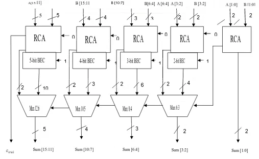
B. PROPOSED SQRT CARRY SELECT ADDER
carry select adder using D-Latch in the place of BEC for the purpose of speed improvement. The conventional SQRT CSLA consists of Ripple carry adder and BEC as shown in Fig.4 whereas RCA or D Latch was used in earlier architectures. The Conventional Group2, Group3 and Group4 structures are shown in Fig.5 which contain full adder, half adder, Binary to Excess1 code Converter and multiplexer units. Conventional SQRT CSLA offers lower delay and high speed than the previous architectures. Fig. 4 shows the block diagram of conventional SQRT CSLA using BEC architecture. First set of RCA is having carry input as ‘0’ and second set is binary to excess-1 converter (BEC). Finally
based on carry input, it selects sum output by using multiplexers. This adder is incorporated in the Wallace Multiplier.
Fig 4, SQRT Carry Select Adder
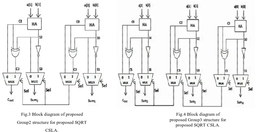
proposed group-2, group-3, group-4 and group-5 structures. Group structure operation is based on only half adders. Sum output is given to an inverter which is stored in 2:1 multiplexer and sum output is given directly for same 2:1 multiplexer. If carry input is’0’, it selects direct sum result or otherwise inverted output as sum. For carry output sum and carry is getting Ex-ored which is given to another 2:1 mux and another input is carry form half adder. If carry input is ‘0’, it selects half adder carry as final carry or otherwise remaining input as final carry. Then Carry output is given to next stage as carry input. The process is continued for group-2, group-3, group-4 and group-5 structures.
A[15:11] B [15:11] A [10:7B [10:7] ] B[6:4] A [6:4] A [3:2] B [3:2] A [1:0] B [1:0]
RCA
RCA
RCA
RCA
RCA
5-bit BEC
4-bit BEC
3-bit BEC
2-bit BEC
Mux 12:6
Mux 10:5
Mux 8:4
Mux 6:3
Sum [15:11] Sum [10:7] Sum [6:4] Sum [3:2] Sum [1:0]
5 5 4 4 3 3 2 2 2 2
2 2
2
2 2
2
10 3 6
4
5 4 3
1 1
1 1
0 0
ISSN(Online): 2320-9801 ISSN (Print) : 2320-9798
I
nternational
J
ournal of
I
nnovative
R
esearch in
C
omputer
and
C
ommunication
E
ngineering
(An ISO 3297: 2007 Certified Organization)
Vol. 4, Issue 10, October 2016
Fig 5 Block diagram of conventional Group2, Group3 and Group4 structures
Fig 6 Block diagram of proposed Group 2 & 3 structure for proposed SQRT CSLA
The performance of reduced complexity SQRT CSLA based Bi-Recoder is better than the performance of compressors adder based Bi-Recoder due to less hardware complexity of reduced complexity SQRT CSLA.Both compressors based digital adder and reduced complexity SQRT CSLA adder is incorporated into the addition part of Bi-Recoder multiplier independently. The performance of reduced complexity SQRT CSLA based Bi-Recoder is better than the performance of compressors adder based Bi-Recoder due to less hardware complexity of reduced complexity SQRT CSLA.
Fig.3 Block diagram of proposed Group2 structure for proposed SQRT
CSLA.
Fig.4 Block diagram of proposed Group3 structure for
proposed SQRT CSLA.
ISSN(Online): 2320-9801 ISSN (Print) : 2320-9798
I
nternational
J
ournal of
I
nnovative
R
esearch in
C
omputer
and
C
ommunication
E
ngineering
(An ISO 3297: 2007 Certified Organization)
Vol. 4, Issue 10, October 2016
V. RESULTS AND DISCUSSION
The FIR filter designs are coded in Verilog hardware description language (HDL) and implemented in FPGA using Xilinx Virtex-5 (xc5vlx50t-1ff1136) as the target device. The Wallace tree and Bi-recoder multipliers are used in sequential and parallel architecture of microprogrammed FIR filters. Simplify pro tool is used for the synthesis, translation, mapping and place-and-route process. Different reports are generated by the CAD tools which are summarized in the tables below. The iteration of synthesis has The FPGA resource utilization table includes Virtex-5 slice look-up tables (LUTs), minimum period and maximum clock frequency. Table I and table I summarizes the implementation results of the sequential FIR filter using Wallace tree and Bi-recoder multipliers respectively.
A. COMPARSION OF WALLACE TREE MULTIPLIER AND BIRECODER MULTIPLIER
The comparsion of Wallace tree multiplier and Birecoder multiplier of power, delay, area. The power is denoted by (mw) its represented in the form of tabular column and its represented by using chart.
Parameters Existing Wallace Tree Multiplier
Proposed Bi-recoder Multiplier
LUTs 144 130
Slices 94 72
Delay 21.440ns 20.165ns
Power(mW) 894mW 746mW
Tab 1- Comparsion of Wallace tree and Bi-recoder Multiplier
0 100 200 300 400 500 600 700 800 900 1000
LUTs Slices Delay (ns) Power (mW)
Existing Wallace Tree Multiplier
Proposed Bi-recoder Multiplier
ISSN(Online): 2320-9801 ISSN (Print) : 2320-9798
I
nternational
J
ournal of
I
nnovative
R
esearch in
C
omputer
and
C
ommunication
E
ngineering
(An ISO 3297: 2007 Certified Organization)
Vol. 4, Issue 10, October 2016
VI. CONCULSION
Digital filters are one of the main elements of DSP. FIR filter which mainly comprises of multiply-accumulate structure is the most commonly used digital filter. Since the performance of FIR Filter mostly depends on the multiplier used, an enhanced and improved multiplier will ameliorate the overall system performance. Wallace tree multiplier was designed and implemented using verilog HDL. This multiplier needs many gates to implement the design. So it takes more area and delay. To propose a new efficient multiplier named as Birecoder multiplier. It is one of the best multiplier in the digital circuit design. This multiplier overcomes the existing multiplier drawbacks.
REFERENCES
[1] S. M. Qasim, M. S. BenSaleh and A. M. Obeid, “Efficient FPGA implementation of microprogram control unit based FIR filter using Xilinx and Synopsys tools,” Proc. of Synopsys Users Group Conference (SNUG), Silicon Valley, USA, pp. 1-14, March 2012.
[2] M. A. Ashour and H. I. Saleh, “An FPGA implementation guide for some different types of serial-parallel multiplier structures,” Microelectroncis J., Vol. 31, PP. 161-168, 2000.
[3] S. M. Qasim, A. A. Telba and A. Y. AlMazroo, “FPGA design and implementation of matrix multiplier architectures for image and signal processing applications,” Int. J. Comp. Sci. Network Security, Vol. 10, No. 2, pp. 168-176, Feb. 2010.
[4] A. M. Obeid, S. M. Qasim, M. S. BenSaleh, Z. Marrakchi, H. Mehrez, H. Ghariani and M. Abid, “Flexible reconfigurable architecture for DSP applications,” Proc. of 27th IEEE Intl. System-on-Chip Conf. (SOCC), pp. 204-209, Sept. 2014.
[5] G. Goto, “High speed digital parallel multiplier,” Nov. 7 1995, uS Patent 5,465,226.
[6] A. D. Booth, “A signed binary multiplication technique,” The Quarterly Journal of Mechanics and Applied Mathematics, vol. 4, no. 2, pp. 236– 240, 1951.
[7] A. Cooper, “Parallel architecture modified Booth multiplier,” Electronic Circuits and Systems, IEE Proceedings G, vol. 135, no. 3, pp. 125–128, 1988.
[8] J. Fadavi-Ardekani, “M*N Booth encoded multiplier generator using optimized Wallace trees,” Very Large Scale Integration (VLSI) Systems, IEEE Transactions on, vol. 1, no. 2, pp. 120–125, 1993.
[9] H. Thapliyal, M. Srinivas, and H. R. Arabnia, “Design and Analysis of a VLSI Based High Performance Low Power Parallel Square Architecture.” in AMCS, 2005, pp. 72–76.
[10] S. Akhter, “VHDL implementation of fast NxN multiplier based on Vedic mathematic,” in Circuit Theory and Design, 2007. ECCTD 2007. 18th European Conference on. IEEE, 2007, pp. 472–475.
BIOGRAPHY
J.Hannah Janet is an M.E scholar in VLSI design in the Electronics and Communication Department, Karpaga Vinayaga College of Engineering and Technology, Affiliated to Anna University. She received B.E degree in 2015 from Anna University, Chennai, Tamil Nadu, and India. Her research interests are Modern VLSI and System on Chip.