TALLEY, MATTHEW LOWELL. High Voltage RFEA Design, Optimization, and Operation in the Cathode of a Dual Frequency Capacitively Coupled Plasma. (Under the direction of Dr. Steven Shannon).
In plasma processing of the semiconductor industry, the ion energy has a significant
effect during the manufacturing process whether it be material deposition, material etch, or ion
implantation. When measuring the ion energy, the results are presented as an ion flux energy
distribution function (IEDf). Since the IEDf has such a strong impact on the manufacturing
process, it becomes necessary to have a detailed and comprehensive understanding of these
effects to properly design the industrial plasma systems suited to the manufacturing process.
Traditionally, IEDfs have been obtained using retarding field energy analyzers (RFEAs) in two
different configurations. The first is where RFEAs are imbedded in a diagnostic wafer that
replaces the process wafer on top of the radio frequency (RF) biased electrode. The second is
where the RFEAs are imbedded in a unique RF biased electrode that is installed in the plasma
system. However, as the semiconductor industry desires to design, characterize, and monitor next
generation plasma systems, a more complete, more accurate, and less invasive measurement
diagnostic is required. The focus of this research was to extend the capabilities of the REFA so
that it could operate in an industrial plasma system under typical manufacturing conditions. This
requires the sensor to be able to measure higher ion energies (i.e. operate at higher potentials)
and handle process gases. To test the concept and feasibility of this type of diagnostic, a typical
RFEA was redesigned for high voltage operation and installed in the RF biased electrode of an
industrial plasma system. The redesign for high voltage operation involved using electrostatic
simulations to optimize the electric field between the grids and increase energy resolution. It was
simulations to analyze the effects of space charge distortion on the current-voltage (IV) curves
and IEDfs obtained by the RFEA. The IEDfs were obtained from the IV curves using a
regularized least-squares (RLS) solution. The space charge distortion was found to be linked to
the grid gap distance and incoming ion flux. A first order model of the space charge potential
was developed to truncate the system matrix of the RLS method to compensate for space charge
distortion. It was found that if the space charge potential can be accurately modelled, the
truncation of the system matrix will provide an undistorted IEDf. To install the RFEAs in the
electrode of an industrial system, a new electrode with a cavity was created to the same outer
dimensions of the industrial electrode it replaced. Multiple probes were installed in the electrode
cavity and IEDf measurements were taken when the electrode was grounded and RF biased. The
IEDfs obtained from the electrode RFEAs for an argon plasma were compared with IEDfs from
a commercial probe under the same plasma conditions. The IEDfs were found to be very similar
to one another showing the redesigned RFEAs were operating correctly. The IEDfs obtained
when the electrode was RF biased displayed the expected bimodal peaks (i.e. saddle shape) at
reasonable energies. IEDfs measurements were also obtained from plasmas with gas mixtures
similar to industrial process mixtures. For these measurements an argon-carbon tetrafluoride or
argon-carbon tetrafluoride-oxygen gas mixture was used. The IEDfs obtained from these plasmas
for an RF biased electrode also showed the expected saddle shape but with additional peaks
caused by ions with different masses. The measurements obtained show it is possible to use this
© Copyright 2018 by Matthew Talley
Capacitively Coupled Plasma
by
Matthew Lowell Talley
A dissertation submitted to the Graduate Faculty of North Carolina State University
in partial fulfillment of the requirements for the degree of
Doctor of Philosophy
Nuclear Engineering
Raleigh, North Carolina 2018
APPROVED BY:
_______________________________ _______________________________ Dr. Steven Shannon Dr. John Muth
Committee Chair
_______________________________ _______________________________ Dr. Alok Ranjan Dr. Katharina Stapelmann
External Member
ii
BIOGRAPHY
iii
ACKNOWLEDGMENTS
I would first like to give my appreciation to Heavenly Father and His Son who have blessed me greatly and given me the faith and strength to become the person I am today. I also cannot express the thanks my wife McKenna deserves for all her support, love, and patience. She has endured even more days waiting patiently for me to finish the last leg of my studies. She has been constant source of encouragement and a listening ear when I need to discuss issues with my research. Her perspective continues to help provide me with insight and has always helped me improve my understanding and clarity when describing my work. I want to thank my parents for all their love and support. I appreciate my father for the example he has set for me as a husband, provider, and man of God as well as his support in all my endeavors. I also have deep gratitude for my mother and the love, help, and nurturing she has provided throughout my life. She has always been there for me no matter the situation. I would not have been able to make it to this point in my education without them.
I could also not have come to this point without the guidance from Steve Shannon. I am
especially appreciative of his willingness to take this wide-eyed student under his wing although
I come from a place (Ohio) he refuses to set foot in. I will always be indebted for all the, time,
knowledge, and experience he has provided to me who started with a bare minimum
understanding of what a plasma is and what can be done with it. I am most grateful for his ability
to make me feel like a peer while discussing the research while also guiding me though my own
thoughts and ideas to come to the most logical conclusion. I am sure that this process he has
taught me will be invaluable in my future work as a researcher and engineer. I also couldn’t have
made it this far without the help from my fellow students, especially Casey Icenhour, Abdullah
Zafar, and Dave Peterson. They have been excellent teachers, study partners, and sounding
iv Lastly, I would like to thank all those at the Austin Plasma Lab (now the Concept and
Feasibility Lab) at TEL. I could not have completed this work without them. Lee Chen, Barton
Lane, Merrit Funk, Peter Ventzek, and Alok Ranjan were all excellent mentors guiding me
through my work there. Mike Hummel was an amazing resource for one who has never had
much experience in designing and manufacturing parts in industry. Joel Blakenly and Zhying
Chen where essential in helping me understand the RFEA diagnostic and previous work that led
up to my own work. Without any of them at this lab, I would not have been able to finish the
v
TABLE OF CONTENTS
LIST OF TABLES ... vii
LIST OF FIGURES ... viii
CHAPTER 1: INTRODUCTION ... 1
CHAPTER 2: EXPRIMENTAL CHAMBER AND RFEA DESIGN ... 30
2.1 RFEA Design ... 30
2.1.1 Electric Field ... 35
2.1.2 Grid Plane Potential ... 45
2.2 Experimental Chamber ... 53
2.2.1 Custom Electrode ... 56
2.2.2 Cavity Electric Fields ... 60
2.2.3 Drift Cone Pressure ... 64
2.3 Measurement Electronics ... 69
2.4 Regularized Least-Squares Solution Method... 70
CHAPTER 3: SPACE CHARGE DISTORTION AND COMPENSATION ... 75
3.1 RFEA Space Charge Distortion ... 75
3.1.1 XPDP1 Simulation ... 79
3.1.2 Simulation IEDfs ... 86
3.2 Space Charge Compensation ... 90
3.2.1 Compensation Models ... 91
3.2.2 Compensation Results ... 100
CHAPTER 4: RFEA WALL AND ELECTRODE MEASUREMENTS ... 103
4.1 Single Frequency Measurements ... 103
4.1.1 RFEA Validation ... 106
4.1.2 IV Curve Characteristics ... 110
4.1.3 Probe Comparison ... 127
4.2 Dual Frequency Measurements... 133
4.2.1 IV Curve Characteristics ... 136
4.2.2 Probe Comparison ... 143
CHAPTER 5: PROCESS CHEMISTRY RFEA MEASUREMENTS ... 161
vi
5.1.1 Ar – CF4 Comparison... 162
5.1.2 Ar – CF4 Probe Comparison ... 165
5.1.3 Ar – CF4 Pressure Ratio Comparison ... 169
5.2 Dual Frequency Measurements... 175
5.2.1 Ar – CF4 – O2 Probe Comparison ... 178
5.2.2 Ar – CF4 Pressure Ratio Comparison ... 189
CHAPTER 6: CONCLUSION... 194
6.1 Design Recommendations ... 199
6.2 Future Work ... 205
REFERENCES ... 214
APPENDICES ... 222
Appendix A: Electron Temperature and Sheath Density Code ... 223
Appendix B: IEDfs Plots with Fewer Curves for Clarity ... 228
vii
LIST OF TABLES
Table 1: This table compares the advantages and disadvantages of each of the different
probes or measurement methods. ... 17
Table 2: Dimensions for the RFEA plates and polyimide sheets. See Fig. 15 - Fig. 17 for a refence for where to apply the dimension. ... 33
Table 3: Pressure, throughput, and ion mean free path for the differential pumping
assembly and electrode. ... 66
Table 4: Density values entering the plasma electron rejection grid compared to density
values from Eq. 9 in chapter 1 presented by Green [ 82 ]. ... 85
Table 5: Boundary conditions used in Eq. 29 to find values for 𝑉𝑖𝑛𝑡 and 𝑉𝑐𝑜𝑛. In these equations, the plasma electron rejection grid is located at x = 0 and the
discriminator is located at x = d. ... 96
Table 6: Values used in the estimation of the true 𝐼𝑠𝑎𝑡 for the 20 mTorr WP measurement. It also presents the values for the 20 mTorr neutral current 𝐼𝑛, the total 20 mTorr
𝐼𝑠𝑎𝑡, and the 5 mTorr 𝐼𝑠𝑎𝑡. ... 121 Table 7: Values used in the estimation of the neutral current (𝐼𝑛) from the 5 mTorr 𝐼𝑠𝑎𝑡
based on the charge exchange collision percentage. This shows the WP pressure, the charge exchange cross-section, the mean free path of the Ar ions, and the
viii
LIST OF FIGURES
Fig. 1: Depiction of the plasma and the boundary layer (sheath) between it and the
chamber surface. How the ion trajectory responds to the sheath can also be seen. ... 2
Fig. 2: Plots depicting the sheath position over time for two different bias frequencies. (a) ω ~ 𝜔𝑝𝑖 (b) ω ≫𝜔𝑝𝑖. ... 4 Fig. 3: Plots presented by Shannon et al. [ 42 ]. (a) shows how the IEDf changes based on
the amount of low frequency current added to a plasma. (b) shows how the bottom width of the etch profile changes in comparison to the top width based on the
percentage of 2MHz power added. ... 6
Fig. 4: Plots presented by Yoshida et al. [ 43 ]. (a) shows how the shape of the IEDf changes when controlling higher order moments by changing the phase between the low frequency power and one of its harmonics. (b) shows how the etch
selectivity changes as the skew of the IEDf changes. ... 6
Fig. 5: Simple schematic of an energy analyzer-mass spectrometer. The dashed arrows represent the flow of particles through the device. In this figure the Energy
Analyzer is a 90° electrostatic energy selector. ... 9
Fig. 6: Simple schematic of a cylindrical mirror analyzer. S represents the particle source, C is the particle collector, L is the distance between them, a and b are the radii of the cylinders, and θ is the angle at which the particles leave from the source. The dashed lines represent the trajectory of the particles. ... 10
Fig. 7: Nonlinear plasma circuit model for a homogeneous RF plasma based off of a figure by Lieberman and Lichtenberg [ 12 ]. The components 𝐶1 and 𝐶2 represent the sheath capacitance. 𝑅1 and 𝑅1 represent the sheath resistance. 𝐼̅𝑖 is the DC
current source that represents ion heating. ... 12
Fig. 8: Diagram of an RFEA. This is a three-grid design and each grid is labeled. The plot on the left represents how the potential changes between each grid as the
discriminator scans. The color of the lines represents the amount of ion current
passing to the collector where red is the highest and blue is the lowest. ... 15
Fig. 9: Example of an IV Curve from an RFEA and the corresponding IEDf. ... 15
Fig. 10: Plots recreated from data presented by Jones [ 85 ]. These plots show that space distortion occurred for 𝑉1 < 150 V or 𝐽 ≤ 1.46 𝑥 10−2 A/cm2. ... 23 Fig. 11: A plot recreated from data presented by Donoso and Martin [ 83 ]. This plot
ix Fig. 12: This is a plot recreated from data presented by Donoso and Martin [ 76 ]. This plot
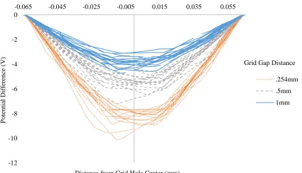
shows the change in the grid hole potential based on the grid gap distance. ... 25
Fig. 13: Plot recreated by data presented by Donoso, Martin, and Puerta [ 75 ]. This plot shows the IV curves obtained when adjusting the grid distance. The shift in the IV curve shape is due to a decrease in the potential drop in the grid holes. ... 26
Fig. 14: Plot recreated from data presented by Landheer et al. [ 34 ]. This plot shows the IEDf created by scanning a monoenergetic beam of 22 eV H3+ ions across the
potential field in the grid holes on a retarding grid for a sweep from 0 to 50 V. The expected peak energy is at 22 eV but the IEDf gives a peak energy at 25 eV. The 3 eV shift is due to the potential sagging in the grid holes. ... 26
Fig. 15: Model of the RFEA design in an isometric view. See Fig. 17 for a detailed view of the honeycomb structure. ... 32
Fig. 16: Slice of the RFEA model. This shows the internal structure as well as labels each grid and the collector. (a) Floating grid (b) Plasma electron rejection grid (c)
Discrimination grid (d) Collector. ... 32
Fig. 17: Closeup of the honeycomb grid in the RFEA. The dashed circle represents the grid fill diameter. The dashed lines form a 60° stagger angle to specify how the holes are aligned in the honeycomb structure. The aspect ratio of the grid holes is 1:1. ... 34
Fig. 18: Section outline of the electron rejection grid (b) and discrimination grid (c). (e)
Gap distance (f) Grid fill diameter (g) Grid hole diameter. ... 35
Fig. 19: Section cut of the RFEA showing the lines from which the 2D electric field plots were generated. The dashed lines represent the locations at which the electric field was measured in the electrostatic simulations. ... 36
Fig. 20: Vertical component (Y) of the electric field down the center of the probe. The
electric field magnitude is measured down the vertical dashed line on the RFEA. ... 38
Fig. 21: Normalized vertical electric field (Y) to the total electric field using the root of the sum of the squares. The electric field values were taken from a vertical line down the probe. ... 38
x Fig. 23: Normalized vertical electrical field (Y) to the total electric field using the root of
the sum of the squares. The electric field values were taken horizontally across the probe between the electron rejection grid and discrimination grid. ... 40
Fig. 24: Variations in the vertical electric field above the discrimination grid. Spurious data from numerical artifacts has been removed for clarity. (a) Variations due to the grid fill diameter where the edge of the plot represents the edge of the
3.175mm fill diameter. (b) Variations due to grid hole diameter. In both plots, the left side of the plot represents the electric field found 0.5mm above the
discrimination grid while the right side represents the electric field found at
0.75mm above the discrimination grid. ... 43
Fig. 25: Variations in the vertical electric field above the discrimination grid. Spurious data from numerical artifacts has been removed for clarity. (a) Variations due to grid gap distance. (b) Variations due to the discrimination potential of the discrimination grid. In (b), the left side of the plot represents the electric field found 0.5mm above the discrimination grid while the right side represents the
electric field found at 0.75mm above the discrimination grid. ... 44
Fig. 26: Comparison of the vertical electric field based on original and optimal geometric parameters. (a) Original geometric parameters (b) Optimal geometric parameters. .... 46
Fig. 27: Plot of the potential in the grid holes of the discrimination grid for an applied
voltage of 500V. Note – the spikes are spurious data due to numerical artifacts. ... 47
Fig. 28: Close-up of the discrimination grid and the location at which the potential was
obtained in the grid holes. ... 48
Fig. 29: The potential difference between the grid plate and grid holes due to the grid gap distance. Spurious data resulting from numerical artifacts has been removed for clarity. ... 50
Fig. 30: The potential difference between the grid plate and grid holes due to the grid hole diameter. Spurious data resulting from numerical artifacts has been removed for clarity. ... 50
Fig. 31: The potential difference between the grid plate and grid holes due to the
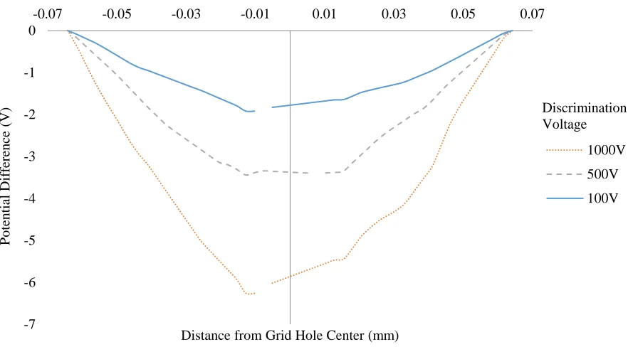
discrimination potential. Spurious data resulting from numerical artifacts has been removed for clarity. ... 51
Fig. 32: Potential profile of a grid. The entrance diameter is where the valley crosses a value of 500 V while the physical diameter is the physical diameter of the grid
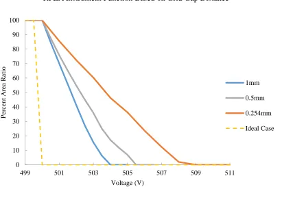
xi Fig. 33: Instrument functions of an RFEA for a monoenergetic (500 eV) ion beam based
on changes in the potential drop in the grid holes. Separate functions were created for the different grid gap simulations. ... 52
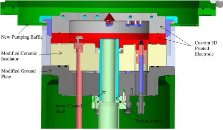
Fig. 34: Pictures of the TEL 200mm DRM chamber. (a) 200mm DRM chamber housing (b) 13MHz matching network (c) Main chamber turbomolecular pump (d) Diagnostic differential turbomolecular pump (e) Feedthrough for RFEAs in the
bottom electrode (f) Bottom electrode cooling lines. ... 54
Fig. 35: Pictures of the TEL 200mm SCCM chamber. (a) 200mm SCCM electrode housing (b) gas box (c) 60MHz matching network (d) Upper electrode cooling
lines. ... 54
Fig. 36: Pictures of the mating piece used to combine the components of the two TEL
chambers. ... 54
Fig. 37: Lower 200mm DRM electrode housing SolidWorks model. This shows the
different components that were added or modified for the RFEA sensors. ... 56
Fig. 38: Pictures of the Si wafer and grid used as the entrance to the electrode RFEAs. (Left) SolidWorks model of the Si grid for a 0.002” (0.05mm) grid hole diameter, 1:1 aspect ratio, 0.003” (0.08mm) spacing, a 60° stagger angle, and 0.125”
(3.175mm) fill diameter (Right) Picture of one of the Si wafers similar to the one used in the following experiments. ... 57
Fig. 39: SolidWorks model of the top portion of the electrode. This picture shows the drift cones (red), cooling channel (teal), drift cone pressure channel (purple), and
tapped holes for wafer and probe connection (green). ... 58
Fig. 40: Pictures of the top half of the actual 3D printed electrode. It shows the drift cones and screw holes for the silicon wafer. (a) Top mount (TM) RFEA (b) Surface mount (SM) RFEA (c) Floating mount (F) RFEA (d) Electrode cooling channels (e) Pressure measurement channel ... 59
Fig. 41: SolidWorks model of the bottom half of the electrode. The face was made transparent so the cooling channels (blue), drift cone pressure channel (purple),
and RF transmission rod connection location (green). ... 59
Fig. 42: Pictures of the bottom half of the electrode. (Right) (a) Screws attaching the RF transmission rod (b) Teflon sleeve (Left) It also shows the incorporation of the RF service plate connections and O-ring seal location (c) Cooling channels (d)
Pressure measurement channel (e) RF rod connection slot. ... 60
xii given the properties of vacuum and a stationary plasma above the electrode
assigned typical plasma electrical properties. ... 62
Fig. 44: RF electric field from the HFWorks simulation at 13.56 MHz and 1 kW of power. SM stands for the surface mount and TM stands for top mount ... 62
Fig. 45: RF magnetic field from the HFWorks simulation at 13.56 MHz and 1 kW of power. A transparent version of the electrode and stationary plasma assembly is visible. SM stands for surface mount and TM stands for top mount. ... 63
Fig. 46: Electrostatic results for an older differential pumping feedthrough design. Here the electric field is strong enough that it will adversely affect the operation of the center RFEA probe. SM stands for surface mount and TM stands for top mount. ... 64
Fig. 47: Electrostatic fields for the DC simulation of the current differential pumping feedthrough design. Here, the field is not strong enough to reach any of the
detectors to adversely affect their operation. SM stands for surface mount and TM stands for top mount. ... 65
Fig. 48: Diagrams of the current (left) and less obtrusive (right) drift cones. Here, θ
represents the half angle for the top portion of the drift cone. ... 68
Fig. 49: Plot comparing the drift cone pressure to changes in the drift cone half angle θ. ... 68
Fig. 50: Diagram of the control electronics for the RFEA measurements. The color code specifies the voltage on the line. Red - high voltage signal, Blue - computer ground, Green - rack ground, Yellow - Collector voltage, Orange - high voltage minus battery bias. ... 70
Fig. 51: Plot of an IV curve and how step functions are used to approximate the IV curve. These step functions are used in the system matrix (𝐾) in the least squares
regularization method. ... 72
Fig. 52: Plot of the L-curve created using multiple regularization parameter (α) values. The curve represents the influence of two competing mechanisms: the exact differentiation of the IV curve and smoothing of the noise in the IV curve. The optimized α is the α value used to create the point in the bend in the L-curve that is closes to the bottom right corner of the plot. ... 73
Fig. 53: Plot of the original IV curve and the IV curve created from the reconstructed IEDf. This plot shows how the noise in the original IV curve is smoothed by the regularization parameter. ... 73
xiii shows that the RLS method provides an accurate solution of the original
distribution. ... 74
Fig. 55: Example of how the shape of the potential in between the plasma electron rejection grid and the discrimination grid change as the potential changes on the discriminator. In the plot, the discriminator is the far right side and the plasma electron rejection grid is the far left side. Since the potential within an RFEA is a state function, the value assigned to the plasma electron rejection grid is arbitrary and has been set to 0 V for this example. The arrow shows the shift in the
maximum potential as the discriminator potential changes. ... 77
Fig. 56: Plot of the potential maximum between the plasma electron rejection grid and the discriminator caused by space charge build-up. The discriminator is located at the left vertical axis and the plasma electron rejection grid is located at the right vertical axis. Since the potential within an RFEA is a state function, the value assigned to the plasma electron rejection grid is arbitrary and has been set to 0 V for this example. This plot was created using XPDP1 [ 62 ]. This curve was created for Ar ions with an incoming current density of 6.8971 A/m2, grid gap
distance of 1.5 mm, drift velocity of 20 eV, and thermal velocity of 5 eV. ... 78
Fig. 57: This is a plot of the Vx-X Phase Space of ions plotted against their position in between the plasma electron rejection grid and the discriminator. In the plot, the discrimination grid is the far left side and the plasma electron rejection grid is the far right side. All the ions below the dashed line are moving to the left while those above are moving to the right. In this instance, the space charge build-up created a potential maximum that was larger than some of the ion energies traversing the space between the grids. Ions with insufficient energy were reflected back even though they had enough velocity to make it through the discriminator. This plot was created from an XPDP1 [ 62 ] simulation. This phase space profile was created for Ar ions with an incoming current density of 6.8971 A/m2, grid gap
distance of 1.5 mm, drift velocity of 20 eV, and thermal velocity of 5 eV. ... 79
Fig. 58: IV curves obtained from the XPDP1 simulations for an incoming current density from a 1x1010 cm-3 plasma density. ... 83
Fig. 59: IV curves obtained from the XPDP1 simulations for an incoming current density from a 1x1012 cm-3 plasma density. ... 83
Fig. 60: IV curves obtained from the XPDP1 simulations for an incoming current density from a 2x1012 cm-3 plasma density. ... 84
Fig. 61: Multiple IV curves for a plasma density of 2x1012 cm-3 showing a smooth
transition as space charge distortion occurs at increasing gap distances... 86
xiv distribution function that XPDP1 used in assigning energies to the ions in the
simulation. ... 87
Fig. 63: Plots the reconstructed IEDfs from the IV curves presented in Fig. 59 for a plasma density of 1x1012 cm-3. The reconstructed IEDfs are plotted along with the original distribution function that XPDP1 used in assigning energies to the ions in the
simulation. ... 87
Fig. 64: Plots the reconstructed IEDfs from the IV curves presented in Fig. 60 for a plasma density of 2x1012 cm-3. The reconstructed IEDfs are plotted along with the original distribution function that XPDP1 used in assigning energies to the ions in the
simulation. ... 88
Fig. 65: Plot of the IEDfs for a 2x1012 cm-3 plasma density for the IV curves presented in Fig. 61. These IEDfs are also plotted with the original energy distribution used in XPDP1 in assigning energies to the ions in the simulation. ... 89
Fig. 66: A plot of the density distribution used in creating a model to truncate the system matrix 𝐾 of the RLS method. To start, a simple step function was used to
represent the density distribution to keep complexity of the model low. ... 92
Fig. 67: Plot of how the lower limit of integration changes with the potential applied to the discrimination grid with and without space charge distortion. In the case there is no space charge distortion, the lower integral limit follows the red line. If there is space charge distortion, the lower integral limit would start at one of the green dots on the vertical axis and trace a path (dependent on the shape of the IEDf) to one of the blue dots on the red line (represented by the orange curve). Knowing the potential 𝜙(𝑥), it is possible to find the intercept voltage (𝑉𝑖𝑛𝑡) (green dots) and the convergence voltage (𝑉𝑐𝑜𝑛) (blue dots). The lighter green line is a simple
linear model between the two potentials that can be used to truncate the system
matrix (𝐾). ... 94 Fig. 68: Comparison of the XPDP1 potential values to the potential values predicted by the
model equation for 𝑉𝑖𝑛𝑡. For this case, a constant thermal energy of 5 eV or a
constant drift energy of 20 eV was used when varying the other parameter. ... 98
Fig. 69: Comparison of the XPDP1 potential values to the potential values predicted by the model equation for 𝑉𝑐𝑜𝑛. For this case, a constant thermal energy of 5 eV or a
constant drift energy of 20 eV was used when varying the other parameter. ... 99
xv Fig. 71: Plot of the maximum space charge potential compared to the applied
discriminator-collector potential for a space charge distortion case. As expected at lower grid potentials, the space charge potential dominates until the applied grid potential is able to overcome the potential produced by space charge build-up. ... 101
Fig. 72: Plot of the maximum space charge potential compared to the applied
discriminator-collector potential for a space charge distortion case. The linear estimation model and four-point estimation model used to truncate 𝐾 that use
points from the measured maximum potential are also plotted. ... 102
Fig. 73: Example of how 𝐾 is truncated using the space charge potentials to compensate for space charge distortion. (a) Original system matrix (b) Truncated system
matrix. ... 102
Fig. 74: Plot of the reconstructed IEDfs. This shows the original IEDf created from the original 𝐾. It also shows IEDfs generated from truncating 𝐾 with the linear and four-point models. An IEDf generated from truncating 𝐾 with the exact space charge potential is also shown. These are compared against the original
distribution used by XPDP1. ... 103
Fig. 75: Pictures of the TEL RFEA wall probe (WP). (Left) Picture of the front of the grid in the wall of the chamber (a) Ground cover that covers the probe and attaches to the differential pumping shaft (b) Port cover to prevent light-up down the outside of the differential pumping shaft (c) Floating (1st) grid (Right) Picture of the WP housing on the outside of the chamber (a) Linear stage that moves the probe in and out of the chamber (b) differential pumping line (c) Bellow that covers the
differential pumping shaft on which the RFEA is mounted. ... 107
Fig. 76: Picture of the Impedans Semion probe attached to the chamber wall ... 107
Fig. 77: Picture of the Impedans Semion filter box rigged to the WP (a) Impedans Semion filter box (b) WP vacuum transition ... 107
Fig. 78: Normalized IEDfs from the TEL RFEAs and the Impedans Semion probe. These measurements were obtained from a 5 mTorr Ar plasma for 400 W 60 MHz RF. The probes were taking measurements at chamber ground. ... 108
Fig. 79: Normalized IEDfs from the TEL RFEAs and the Impedans Semion probe. These measurements were obtained from a 5 mTorr Ar plasma for 700 W 60 MHz RF. The probes were taking measurements at chamber ground. ... 109
Fig. 80: IV curves taken with the WP for a 40 mTorr Ar plasma for 300 W 60 MHz RF source. (a) In this measurement, the plasma electron rejection (2nd) grid was set to -50 V. (b) In this measurement, the 2nd was set to -100 V. The first drop-off
xvi Fig. 81: SolidWorks model of the new WP assembly. It shows the expanded ground cover
so now differential pumping does not have to occur through the probe but can
pass around it. ... 113
Fig. 82: Pictures of the new WP. (Left) Picture of the new WP at the inner chamber wall (a) New ground cover that no longer requires the port cover to prevent light-up down the outside of the differential pumping shaft (b) Grid machined into the ground cover that acts as the main differential pumping limiter (Right) Picture of the RFEA mounted to the modular differential pumping shaft (a) Screw
connection to attach the ground cover (b) Openings to allow for pumping around the probe ... 114
Fig. 83: Plot of two IV curves based on the bias applied between the discrimination grid and the collector. A linear trend is seen in the ion saturation current region up until 0 V or 9 V. The arrows approximately point to these two locations. These are the moments that the collector becomes positive so ions outside the probe are no longer attracted to the collector. ... 115
Fig. 84: Picture of the ion beam expansion around the drift cone. It also represents that ions outside the RFEA will be picked up by the collector when it is negatively
biased. ... 117
Fig. 85: Picture of the top mount (TM) probe with a Vespel SP-1 cover (a) around the collector. These covers were placed not only on this RFEA, but also the floating probe (F) and new wall probe (WP) to prevent ion current from being collected
outside the detector. ... 117
Fig. 86: Zoomed in plot of IV curves obtained with the new WP for 20 mTorr Ar at different 60MHz RF powers. It can be seen here that the no ion current region is relatively flat but there seems to be an increasing offset of the IV curve from 0 A. This offset is due to secondary electron emission off the collector due to fast
neutrals entering the probe. ... 119
Fig. 87: IV curve comparison for WP measurements at two different pressures and different RFEA operation modes. The 4GM stands for four grid mode where a secondary electron rejection grid was used in between the discriminator and the collector. The 3GM stands for three grid mode which is the normal operation used in this work. ... 121
Fig. 88: Plot of the IV curves obtained from for an Ar plasma at different pressure and constant power (Top) IV curves measured using the WP for an Ar plasma generated by 400 W 60 MHz RF. (Bottom) IV curves measured using the SM probe for an Ar plasma generated by 200 W 60 MHz RF. In both cases, the 𝐼𝑠𝑎𝑡
xvii Fig. 89: Plot of density vs. power at different pressures obtained through hairpin
measurements at the center of the chamber. Plasma was generated using 60 MHz power applied to the top electrode. The results show an increase in density with increasing pressure until the 40mTorr measurements. ... 127
Fig. 90: IEDfs from the WP and SM probes for 5 mTorr Ar at different 60 MHz RF
powers and a grounded electrode (GE). The SM probe has IEDf peak energies that seem to be about 10 eV lower than the WP probe. The shapes of the IEDfs are
generally consistent. ... 128
Fig. 91: IEDfs from the TM and F probes for 5 mTorr Ar at different 60 MHz RF powers and a grounded electrode (GE). The IEDf peak locations are very consistent between the TM and F probes. The shapes of the IEDfs are generally consistent but the TM and F probes. ... 129
Fig. 92: IEDfs obtained from the WP probe from an Ar plasma for 200 W 60 MHz RF and a bottom grounded electrode (GE). ... 131
Fig. 93: IEDfs obtained from the SM probes from an Ar plasma for 200 W 60 MHz RF
and a bottom grounded electrode (GE). ... 131
Fig. 94: IEDfs obtained from the TM probes from an Ar plasma for 200 W 60 MHz RF and a bottom grounded electrode (GE). The low energy collisional tail of the TM peak is wider again. The IEDf for the TM probe at higher pressures gets lost in the noise after 15mTorr. ... 132
Fig. 95: Picture of the Impedans Semion filter box attached the one of the electrode RFEA probes. ... 135
Fig. 96: Picture of the Allen Avionics filters attached to one of the electrode RFEA probes. 135
Fig. 97: Dual Frequency IV curves obtained using the SM detector for a 5 mTorr 400 W 60 MHz Ar plasma. The Impedans Semion filter box was used in these
measurements. As the bias power increased, the offset of the IV curve became
more negative. ... 137
Fig. 98: IV curves obtained with the SM probe using two different RF chokes for a 5 mTorr 400 W 60 MHz 70 W 13.56 MHz Ar-CF4-O2 plasma with a 90-5-5
pressure ratio. In the plot, the Impedans Semion filter (Imp.) IV curve has a negative offset while the Allen Avionics (AA) filter IV curve has the expected
positive offset for the same plasma conditions. ... 138
Fig. 99: Plot of the IV curves obtained using the SM, TM, and F probes for a 5 mTorr 400 W 60 MHz 70 W 13 MHz Ar plasma. The plot shows that the shape and current values of the TM probe and F probe IV curves deviates significantly from the
xviii Fig. 100: SolidWorks section model of the TM probe below the drift cone. The section shot
shows how the collector screws are exposed to the cavity allowing for current
collection. ... 142
Fig. 101: Comparison of the IEDfs not shifted based on VDC from the IV curves in Fig. 100 taken by the SM, TM, and F probes. As expected, the SM IEDf has reasonable peak energy values and shows the typical saddle shape expected of a dual
frequency IEDf. The TM probe also shows dual peaks in agreement with the SM IEDf but the saddle shape of the IEDf is slightly off. The F probe has a small saddle shape, but the peak locations are very different from the SM and TM peak locations. This probe does not appear to obtain a correct measurement. ... 144
Fig. 102: IEDfs from a 5 mTorr Ar plasma generated by a 400 W 60 MHz RF signal when varying the 13.56 MHz bias power. The WP IEDfs are mainly single peak with hints of dual peak formations due to the fact that the measurement was made at a grounded surface. ... 147
Fig. 103: IEDfs from a 5 mTorr Ar plasma generated by a 400 W 60 MHz RF signal when varying the 13.56 MHz bias power. The IEDfs from the SM have dual peaks as the measurement was made at the bias electrode. For a clearer picture of the trends of the SM IEDf plot at lower powers, see Appendix B. ... 148
Fig. 104: IEDfs from a 5 mTorr Ar plasma generated by a 400 W 60 MHz RF signal when varying the 13.56 MHz bias power. The IEDfs from the TM have dual peaks as
the measurement was made at the bias electrode. ... 148
Fig. 105: IEDfs from a 5 mTorr Ar plasma generated with a -120 V VDC when varying the 60 MHz source power. The WP IEDfs are mainly single peak due to the fact that the measurement was made at a grounded surface. ... 152
Fig. 106: IEDfs from a 5 mTorr Ar plasma generated with a -120 V VDC when varying the 60 MHz source power. The IEDfs from the SM have dual peaks as the
measurement was made at the bias electrode. ... 153
Fig. 107: IEDfs from a 5 mTorr Ar plasma generated with a -120 V VDC when varying the 60 MHz source power. The IEDfs from the TM have dual peaks as the
measurement was made at the bias electrode. For a clearer picture of the trends of the TM IEDf plot, see Appendix B. ... 153
xix Fig. 109: IEDf obtained from the SM probe for an 80 mTorr Ar plasma at 400 W 60 MHz
70 W 13.56 MHz. Two interesting characteristics here. The first is that the red arrow points to a peak that is dependent on the 2nd grid potential. The second is
that after shifting the curve for the VDC, the real peak still appears to be negative. ... 157
Fig. 110: Plot of IEDfs from the SM probe for a 5 mTorr Ar plasma at 200 W 60 MHz 70 W 13 MHz -189.2 VDC. The 2nd grid potential was varied for the different
measurements. The expected saddle shaped peak is obtained but, based on the 2nd
grid potential applied, a third peak is generated at this potential. ... 158
Fig. 111: IEDfs obtained with the WP and SM probe for a 5 mTorr Ar plasma at 400 W 60 MHz and a bottom floating electrode. (a) WP IEDf that represents the ion energy gained from Vp to ground (b) SM IEDf that was shifted for VDC but is in the
negative energy region ... 159
Fig. 112: Plots of the shifted SM IEDf curves. (a) The original IEDf shifted by VDC (b) The new IEDf shifted by Vp – Vf. Shifting by Vp – Vf now puts the SM IEDf in the
positive region. ... 160
Fig. 113: IEDfs recreated from data presented by Donko and Petrović [ 93 ]. This plot shows the IEDf for Ar+ and CF4+ ions for a simulated 20 mTorr CCP with a 100
MHz 60 V source and grounded secondary electrode. ... 163
Fig. 114: Plots of the normalized measured IEDfs compared against the normalized simulations results presented by Donko and Petrović. [ 93 ] (a) IEDfs from the SM and F probes (b) IEDf from the TM probe. Two plots were made for clarity due to the noisy nature of the TM IEDf. ... 164
Fig. 115: Plots of IEDfs obtained from the WP and SM probes for a 20 mTorr 90-10 Ar-CF4 plasma at different 60 MHz source powers. The SM probe was housed in a grounded electrode (GE) during these measurements. ... 166
Fig. 116: Plots of IEDfs obtained from the TM and F probes for a 20 mTorr 90-10 Ar-CF4 plasma at different 60 MHz source powers. The TM and F probes were all housed in a grounded electrode (GE) during these measurements. The 500 W TM IEDf (See Fig. 114 (b)) was removed from the TM IEDf plot for clarity. For a clearer picture of the trends of the WP IEDf plot at lower powers, see Appendix B. ... 167
Fig. 117: Plot comparing the IEDfs from the WP, SM, TM, and F probes for a 20 mTorr 90-10 Ar-CF4 plasma with a 400 W 60 MHz RF source. The peak energies line up
xx Fig. 118: Plots of the IEDf based on the pressure ratio of Ar-CF4 from the WP and SM
probes. The plasma was generated using either 400 W or 200 W from the 60 MHz source. The bottom electrode was grounded (GE). ... 171
Fig. 119: Plot of the IEDfs obtain by the WP for a 20 mTorr and 40 mTorr Ar – CF4 plasma
generated by a 400 W 60 MHz RF source. The bottom electrode was grounded
(GE) during these measurements. ... 173
Fig. 120: Plot of the ion density taken using a hairpin resonator probe at two different pressures for a Ar-CF4 plasma. In this case, only the 60 MHz source was used,
and the bottom electrode was floating. ... 175
Fig. 121: Plots of the IEDfs obtained from the WP for a 5 mTorr 90-5-5 Ar – CF4 – O2
plasma generated by a 400 W 60 MHz RF source. The 13.56 MHz RF source
power was varied between 25 W and 150 W. ... 179
Fig. 122: Plots of the IEDfs obtained from the SM probe for a 5 mTorr 90-5-5 Ar – CF4 –
O2 plasma generated by a 400 W 60 MHz RF source. The 13.56 MHz RF source
power was varied between 25 W and 150 W. For a clearer picture of the trends of the SM IEDf plot at lower powers, see Appendix B. ... 179
Fig. 123: Plots of the IEDfs obtained from the TM probe for a 5 mTorr 90-5-5 Ar – CF4 –
O2 plasma generated by a 400 W 60 MHz RF source. The 13.56 MHz RF source
power was varied between 25 W and 150 W. ... 180
Fig. 124: IEDfs obtained from the WP for a 5 mTorr 90-5-5 Ar – CF4 – O2 for a constant
-120V VDC. The 60 MHz RF source power was varied between 100 W and 600 W. . 182
Fig. 125: IEDfs obtained from the SM probe for a 5 mTorr 90-5-5 Ar – CF4 – O2 for a
constant -120V VDC. The 60 MHz RF source power was varied between 100 W
and 600 W. ... 182
Fig. 126: IEDfs obtained from the TM probe for a 5 mTorr 90-5-5 Ar – CF4 – O2 for a
constant -120V VDC. The 60 MHz RF source power was varied between 100 W
and 600 W. ... 183
Fig. 127: IEDfs obtained with the WP for a 5 mTorr Ar and 5 mTorr Ar – CF4 – O2 at a 400
W 60 MHz RF source power and a -120 V VDC on the bias electrode. ... 185
Fig. 128: IEDfs obtained with the SM probe for a 5 mTorr Ar and 5 mTorr Ar – CF4 – O2 at
a 400 W 60 MHz RF source power and a -120 V VDC on the bias electrode.
Arrows point out peaks from different ion species in the SM measurement. ... 185
Fig. 129: IEDfs obtained with the TM probe for a 5 mTorr Ar and 5 mTorr Ar – CF4 – O2 at
xxi species but these are uncertain as they are not as distinct. The same color arrows point to peaks generated by the same ion species. ... 186
Fig. 130: Plot of the SM IEDfs at two different bias powers for a 5 mTorr Ar – CF4 – O2
plasma generated by a 400 W 60 MHz RF source. The plot shows a transition between a four peak IEDf to a dual peak IEDf. The transition is caused by a
shrinking of the sheath. ... 188
Fig. 131: IEDfs obtained from the wall probe for a 90-5-5 Ar – CF4 – O2 plasma generated
by a 400 W 60 MHz RF source. The pressure was varied between 5 mTorr and 20 mTorr. The 13.56 MHz bias power was also varied between 50 W and 70 W. ... 189
Fig. 132: Plots of the IEDfs obtained with the WP where the CF4 concentration was
adjusted for a Ar – CF4 plasma when the 60 MHz RF source power was held
constant and the VDC was held constant. A pressure of 20 mTorr and 40 mTorr were used. The 13.56 MHz RF bias power chosen in the constant 60 MHz case was 70 W. The 60 MHz RF source power chosen in the constant -120 V VDC case was 400 W. ... 191
Fig. 133: Radial plasma density profiles obtained from a hairpin resonator probe for a 90-10 Ar – CF4 plasma generated by a 400 W 60 MHz RF source and 70 W 13.56 MHz
bias. The pressure was varied between 10 mTorr and 40 mTorr. ... 193
Fig. 134: Picture of the hairpin resonator probe (or hairpin) and corresponding port cover in the chamber wall. The port cover was designed to allow the hairpin to move in and out while trying to prevent light-up in the hairpin housing connected to the
chamber wall ... 194
Fig. 135: Normalized IV curves that show signs of space charge distortion obtained from the old wall probe (WP) from a 5 mTorr Ar plasma created by a 500 W 60 MHz RF top electrode and a grounded bottom electrode. The gap distance between the plasma electron rejection grid and discriminator was increased from 1 mm to 6
mm. ... 207
Fig. 137: Plot of the z-r phase space for Ar ions in the drift cone. This plot shows the
expansion of the Ar ion flux as it travels the length of the drift cone. ... 209
Fig. 138: Plot of the potential moving from the plasma, through the presheath, and then to the wall. This figure is modeled after the one presented by Lieberman and
1
CHAPTER 1: INTRODUCTION
Plasma processing is a major component in the semiconductor industry. As such, the
semiconductor industry is consistently trying to understand and measure the basic properties of
the plasmas used in the manufacturing process. The one-dimensional ion velocity impinging on
the substrate is one such property. In order to picture the one-dimensional ion velocity impinging
on the substrate from the plasma, an ion velocity distribution function is obtained through
diagnostic measurement and modelling. This is typically presented in the form of an ion flux
energy distribution function. The ion flux energy distribution function allows for a more direct
comparison to other characteristic plasma parameters and variables being considered (e.g.
plasma potential, measurement diagnostic operating potential, cathode peak-to-peak voltage and
direct current (DC) bias, electron temperature, material interactions, etc.) [ 1 - 7 ]. This
distribution function is often referred to, although incorrect, as the ion energy distribution
function (IEDf) [ 8 ]. For consistency with the nomenclature used in the majority of the
referenced material in this thesis, the ion flux energy distribution function will be referred to as
the IEDf throughout.
Plasmas used in materials processing rely primarily on the reactive chemistries formed in
the bulk volume of the plasma region through electron impact, and the energetic, directional ions
that bombard the plasma facing surfaces after being accelerated through the plasma’s boundary
layers. This thesis focuses on the measurement of the latter. During plasma formation of a DC or
radio frequency (RF) electropositive discharge, the majority of the energy is being supplied to
the electrons and with a small fraction going to the ions from the DC or RF electric field. This is
due to the much smaller electron mass and their higher mobility. Therefore, they leave the
2 in the plasma charging positively with respect to ground. The plasma’s boundary layers, called
sheaths, form between the positive quasineutral state of the plasma and the chamber surfaces that
reside at a different potential (See Fig. 1). The sheath is where the largest electric fields reside,
and the source of anisotropic trajectory and energy gain of the ions used in industrial processes.
Fig. 1: Depiction of the plasma and the boundary layer (sheath) between it and the chamber surface. How the ion trajectory responds to the sheath can also be seen.
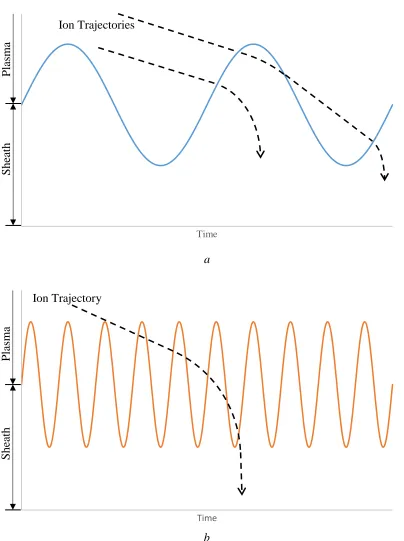
For an RF sheath, which is typically found in industrial systems, the dynamics and effects
on the IEDf are a bit more complicated than a DC sheath where all the ions gain the same
amount of energy. In an RF sheath, the sheath oscillates in size between sheath expansion and
sheath collapse as a response to the oscillation of the RF waveform on the powered electrode.
Depending on the frequency of the powered electrode and the mass of the ions, the ion trajectory
and ion energy will change [ 9 - 12]. To illustrate the effect of the electrode frequency (𝜔) on the ion trajectory and energy, a simple figure was created (See Fig. 2). In Fig. 2 the ion mass is
assumed to be the same between both (a) and (b) and only 𝜔 is changed. The plasma ion frequency (𝜔𝑝𝑖) is used for comparison to 𝜔 where:
Chamber Surface
P
lasma
Shea
th
Ion Trajectory
3
𝜔𝑝𝑖 = √ 𝑒2𝑛
𝑖 𝜀0𝑚𝑖
1
In Eq. 1, 𝑛𝑖 is the ion density and 𝑚𝑖 is the ion mass. The comparison of 𝜔 to 𝜔𝑝𝑖 represents whether the ions are responding to an instantaneous electric field or a time-averaged electric
field. This is due to the fact that the ion transit time (𝜏𝑖) is approximately equal to 𝜔𝑝𝑖−1 and depending on how long the ions remain in the sheath determines if they see a changing electric
field [ 9, 10]. Therefore, in Fig. 2 (a), the ions respond to instantaneous changes in the electric
field in the sheath. This means that the time and trajectory of the ion as it enters the sheath has a
significant impact on the energy the ion gains. In this case, it is possible for an ion to enter the
sheath while the sheath is close to its maximum height only to be over taken by the boundary as
the sheath collapses. This ion will have a significantly different energy than one that enters the
sheath and is never overtaken. Looking at Fig. 2 (b) now, 𝜔 in this case is much larger than 𝜔𝑝𝑖.
Under these conditions, the ions do not respond to the instantaneous changes, but they respond to
the time-averaged electric field changes. This means that the ion energy is much less sensitive to
the time and trajectory at which the ions enter the sheath. As such, the sheath dynamics have a
significant impact on the ion energy and therefore the IEDf and its shape.
Just as changing from a DC to an RF sheath can change the IEDf and its shape, other
methods have been devised to further control the IEDf and adjust its skew. As the frequency of
the RF waveform has a significant impact on the IEDf, the shape of the waveform can also have
a significant effect [ 11, 13]. The data presented by Rauf showed that a sinusoidal waveform
gives a high energy peak with a gentle decreasing slope with decreasing energy. The data for a
4 IEDf. Another very common method to control the IEDf is to use multiple frequencies for the
discharge. The most widely used version in industry is to use two frequencies, one as the
a
Fig. 2: Plots depicting the sheath position over time for two different bias frequencies. (a) ω ~𝜔𝑝𝑖 (b) ω≫𝜔𝑝𝑖.
Time
Time
P
lasma
S
he
ath
b Ion Trajectory
P
lasma
S
he
ath
5 source power and a separate applied as a bias to the substrate. The two frequencies essentially
decouple the density and IEDf making it possible to control the IEDf with the bias frequency [ 2,
3, 5, 10, 11, 13 - 23]. For a constant plasma density, adjusting the RF bias power applied to the
substrate will shrink or expand the overall length of the sheath. If the sheath gets smaller, the ion
travel time across the sheath decreases so they respond to the instantaneous electric field of the
sheath. On the other hand, if the sheath expands, the ion travel time increases which means they
trend more towards the time-averaged electric field of the sheath. Lastly, another method to
control the IEDf and its skew is done by adding a second frequency component to the bias
frequency applied to the substrate. This second frequency is a harmonic to initial RF waveform
and is phase locked so that the two waveforms stay at a consistent phase difference [ 2, 24 ]. By
changing the phase difference between the bias waveform and its harmonic between 0° and 180°,
it is possible to adjust the skew of the IEDf (See Fig. 4). By using these methods, it is possible to
alter the IEDf and its skew which plays a key role in material processing.
The IEDf plays a significant role in the manufacturing process being performed whether
it be material deposition, material etch, or ion implantation [ 2, 3, 5, 8, 10 - 16, 23, 25 - 41].
Within each of these processes, the IEDf has a significant impact on the critical details of the
manufacturing processes such as the amount of heat transferred to the surface during material
deposition, the depth and shapes of the channels during the etch process (See Fig. 3), the
selectivity of material during etching (See Fig. 4), and the depth at which ion implantation stops
just to name a few.
Since the IEDf has such an effect on the manufacturing processes, it becomes necessary
to have a detailed and comprehensive understanding of these effects to properly design plasma
6
PR 4225A
BARC 840A
BPSG Oxide 20000A
Si
0.18-0.2um
Bottom CD
a b
Fig. 3: Plots presented by Shannon et al. [ 42 ]. (a) shows how the IEDf changes based on the amount of low frequency current added to a plasma. (b) shows how the bottom width of the etch profile changes in comparison to the top width based on the percentage of 2MHz power added.
a b
Fig. 4: Plots presented by Yoshida et al. [ 43 ]. (a) shows how the shape of the IEDf changes when controlling higher order moments by changing the phase between the low frequency power and one of its harmonics. (b) shows how the etch selectivity changes as the skew of the IEDf changes.
forward with research on microcircuit designs made on silicon wafers using plasmas, it is all the
more important to utilize the knowledge of IEDf process effects in the development of the new
generation of plasma systems that will be used to make these future microcircuits. One particular
7 implantation process [ 12, 35 - 38 ]. Manufacturers that use either of these processes have been
requiring plasma systems that provide higher ion energies that reach the substrate. They are also
looking for ways to obtain better estimations or measurements of the IEDf during process
conditions. Just as the plasmas systems are evolving, there is a growing need to broaden the
capabilities and application of diagnostics that provide the IEDf.
The objective of this research is to extend the capabilities of an established ion energy
measurement diagnostic to provide a more complete, more accurate, and less invasive
measurement technique desired by the semiconductor fabrication industry to design,
characterize, and monitor next generation plasma systems. The sensor’s design must allow for
operation in the regimes required by manufacturers. This sensor should also be able to measure
the IEDf of a plasma during process conditions or in a scenario that is very similar to process
conditions and not rely on surrogate gases that may not accurately represent actual process
conditions. This includes the ability of the diagnostic to handle process gases. There are a few
diagnostics to be discussed later that meet these requirements but in order to meet this goal, it
was decided that whichever diagnostic is used, will be placed inside a cavity below the surface of
the biased RF electrode of an industrial system on which the substrate sits. This will make it
possible to run with conditions similar to manufacturing process conditions while a silicon wafer
can sit on top of the electrode during the time of the measurements. It also makes it possible to
leave the rest of the industrial chamber minimally modified, with diagnostic and manufacturing
capabilities provided simultaneously by one of these sensors for the first time. By fulfilling these
objectives, the newly modified diagnostic will be able to provide the IEDf for a broader set of
8 A diagnostic must be chosen that can provided the IEDf of a plasma. Multiple diagnostics
and methods have been created to measure and calculate the IEDf. The most common
diagnostics and methods to obtain the IEDf from a plasma are to use an energy analyzer-mass
spectrometer, a sheath or circuit model in a simulation which is compared to direct IEDf
measurements or these models are used in connection with other diagnostics that do not measure
ion velocity directly to calculate the IEDf, and a retarding field energy analyzer (RFEA). Each
diagnostic or method has its advantages and disadvantages, but all provide an IEDf. The
following is a brief overview of the design and operation of each along with a summary of some
results obtained using each diagnostic.
Energy analyzer-mass spectrometers (See Fig. 5) have been used extensively to obtain
particle energy or particularly, the IEDf of a plasma [ 8, 15, 17, 18, 40, 44 - 56]. However, as the
second half of the name suggests, mass spectrometers were originally designed to determine the
mass of different unknown species in a gas mixture. The most common energy analyzer-mass
spectrometer design comes with three distinct regions or parts: an ionizer, an energy analyzer,
and a quadrupole residual gas analyzer (See Fig. 5). To distinguish the energy and mass of the
different species in a neutral gas, particles in the neutral gas mixture are ionized by an electron
gun. However, when used with a plasma, the ionization of the gas species has already taken
place, so this portion of the system is typically turned off or removed from the system.
To distinguish the ion energy of the newly ionized particles, the energy analyzer-mass
spectrometer deflects the trajectory of the incoming ions around a single (e.g. a 45° - 90°
electrostatic energy selector [ 47 - 49, 51, 52 ], See Fig. 5) or multiple bends (e.g. a cylindrical
mirror analyzer [ 46, 50 ], See Fig. 6). Since the ability of an ion to change its trajectory is
9 Fig. 5: Simple schematic of an energy analyzer-mass spectrometer. The dashed arrows represent the flow of particles through the device. In this figure the Energy Analyzer is a 90° electrostatic energy selector.
only ions with a specific momentum and charge pass through the bend or bends without hitting
any other surface. This discrimination process may not be unique to a single momentum and
charge combination though, so a quadrupole residual gas analyzer is also used to discriminate
further in a similar process of the energy analyzer. In order to remove velocity from this
discrimination process, all of the incoming ions are accelerated to the same velocity.
The quadrupole analyzer is made of four parallel metal rods where rods opposite from
one another are electrically connected. An RF signal with a DC offset is applied between the
different pairs of rods. As the ions pass through the quadrupole analyzer only those with a
specific mass-to-charge ratio pass through the analyzer without colliding with the rods or wall.
This makes it possible to collect only ions with a specific mass-to-charge ratio. By knowing the
mass, the charge, and the strength of the deflecting field of the energy analyzer, it is possible to
calculate the incident ion velocity. By taking measurements when sweeping the strength of the
deflecting field, it is then possible to generate and IEDf for the plasma.
Using an energy analyzer-mass spectrometer Janes and Huth [ 45 ] were able to obtain
the IEDf and ion angular distribution function (IADf) at the surface of a RF powered electrode in Ionizer
Energy
Analyzer Quadrupole
10 Fig. 6: Simple schematic of a cylindrical mirror analyzer. S represents the particle source, C is the particle collector, L is the distance between them, a and b are the radii of the cylinders, and θ is the angle at which the particles leave from the source. The dashed lines represent the trajectory of the particles.
a capacitively coupled plasma (CCP) allowing them to investigate the effects of argon ion
collisions within the sheath. Their results showed distinct peak structures in the IEDf resulting
from ions created through charge exchange collisions responding to the RF modulated electric
field of the sheath. The results also show that for pressures greater than 30mTorr, multiple
scattering events become more significant in the development of the IEDf. Their results for the
IADf show that a maximum in peak intensity is obtained at 0° in reference to the surface normal
and intensities found at angles between ±3° are the result of elastic scattered ions.
Mizutani et al. also used an energy analyzer-mass spectrometer to look at how the
operational mode of the energy analyzer changes the shape of the IEDf when taking a
measurement at the surface of a RF powered electrode [ 50 ]. When taking a measurement, there
are two modes in which the energy analyzer can be run: a DC mode and an RF mode. For the DC
mode, the electric potential of the analyzer remains constant while in the RF mode, the electric
potential of the analyzer oscillates with the same frequency, amplitude, and phase present on the
RF electrode. Their results show that an energy analyzer running in RF mode produces the
expected saddle shape (dual) peak formation. A saddle shape peak was also produced when
running in DC mode, but multiple other peaks of a distinguishable intensity were also observed a
b
S C
θ
11 in the continuum region. For the DC mode, there was also a significant shift in the peak location
of the high energy peak compared to the RF mode results. Their results show the necessity to run
an energy analyzer in RF mode when used to measure the IEDf incident on a RF powered
electrode.
Another common method to obtain the IEDf of a plasma is to develop a sheath or circuit
model (See Fig. 7) for the plasma. These models predict the spatiotemporal sheath dynamics
during process conditions to determine the IEDf in the bulk plasma or IEDf incident on the
silicon wafer surface [ 1, 2, 5, 7, 10, 12 - 15, 23, 25, 30, 32, 39, 57 - 63]. These models typically
use a combination of Poisson’s equation, energy conservation, flux continuity, Boltzmann’s
relation, and ion transit time (See Eqs. 2 - 6) [ 10, 12, 63] in describing ion transport and energy
through the sheath. The combination of these equations gives the first necessary component in
creating a model to obtain an IEDf.
∇2Φ =−𝜌
𝜀0 2
1 2𝑚𝑖𝑢
2(𝑥) =1 2𝑚𝑖𝑢𝑠
2− 𝑒Φ(𝑥)
3
𝑛𝑖(𝑥)𝑢(𝑥) = 𝑛𝑖𝑠𝑢𝑠 4
𝑛 = 𝑛0exp(−𝛷 𝑇⁄ ) 5
𝜏𝑖 = 3𝑠√𝑚𝑖⁄(2𝑒𝑉𝑠ℎ)≈ 𝜔𝑝𝑖−1 6
The second necessary component of the model is to properly represent the dependence of
the IEDf on the RF power and frequency. As mentioned earlier, the frequency and magnitude at
which the bias power is provided to the substrate are the major controlling factors of the sheath
dynamics. This means that the frequency and magnitude applied has a direct impact on the
12 applied through the resistive (𝑅) and reactive (𝐶, 𝐿) components of the plasma circuit model (See Fig. 7). By developing this equivalent circuit model of the sheath and coupling it with
particle transport equations through the sheath it is possible to estimate the IEDf that reaches the
substrate. To get the necessary input parameters for the circuit model and particle transport
equations, other diagnostics such as voltage-current (VI) probes, capacitive probes, and Faraday
cups are used to measure the input quantities. From there, it is possible to obtain the IEDf for a
plasma at specific operating conditions.
Fig. 7: Nonlinear plasma circuit model for a homogeneous RF plasma based off of a figure by Lieberman and Lichtenberg [ 12 ]. The components 𝐶1 and 𝐶2 represent the sheath capacitance. 𝑅1 and 𝑅2 represent the sheath resistance. 𝐼̅𝑖 is the DC current source that represents ion heating.
Panagopoulos and Economou were able to make affective use of a plasma sheath model
to simulate the IEDf dependence on the ion modulation (𝜔𝜏𝑖) in the sheath [ 10 ]. Using Eqs. 2 - 6 coupled to the waveform function at the wall (𝑉𝑤) coming from the RF generator, an equation for the damped wall potential (𝑉̅̅̅)𝑤 was obtained (See Eq. 7). Based on the value of 𝜔𝜏𝑖, the 𝑉̅̅̅𝑤
𝐼𝑅𝐹 𝐶𝑝 𝐶1
𝑅1
𝐶2 𝑅2
𝑅𝑝
𝐼𝑖
̅ 𝐼̅𝑖
13 mimics 𝑉𝑤 very closely or deviates quite a bit from 𝑉𝑤. By using 𝑉̅̅̅𝑤, they were able to simulate
the IEDf that would be generated for different values of 𝜔𝜏𝑖. The simulation showed that for
small values of 𝜔𝜏𝑖, a bimodal IEDf is generated with a wide dispersion between the peak energies. When the value of 𝜔𝜏𝑖 got larger, the dispersion between the energy peaks became smaller. Eventually, the IEDf switched from a bimodal peak distribution to a single peak
distribution at sufficiently high values of 𝜔𝜏𝑖. 𝑉𝑤
̅̅̅(𝑡) = 𝑉𝐷𝐶+ ∑ 𝑉𝐴𝐶𝑗 1 + (𝑗𝜔𝜏𝑖)2
[cos(𝑗𝜔𝑡 + 𝜃𝑗) + (𝑗𝜔𝜏𝑖) sin(𝑗𝜔𝑡 + 𝜃𝑗)] 𝑗
7
Sobolewski, Wang, and Goyette also used a plasma sheath model when looking at the
IEDf of an RF inductively coupled plasma (ICP) composed of only CF4 [ 15 ]. In contrast to
Panagopoulos and Economou, they used a less complex sheath model in conjunction with
experimental data from a Faraday cup and capacitive probe to obtain an IEDf at an RF biased
surface. They assumed their sheaths were consistent with a matrix sheath model where the
electron density profile is step function at the plasma sheath interface. This simplifies Poisson’s
equation allowing them to avoid an iterative solution for electron density. The IEDf from the
sheath model was also compared to the IEDf obtained from an energy analyzer-mass
spectrometer that was attached at the chamber wall. Even though the spectrometer was grounded,
it was positioned close to the RF biased electrode so that the sheath in front of the spectrometer
developed an RF voltage when RF power was applied to the electrode. This made it possible to
study RF bias effects with the spectrometer and compare the results with the sheath model.
The results from the model were found to be quite accurate with the IEDf measured by
the spectrometer. The results show three different types of behavior depending on the frequency
applied to the biased electrode. For frequencies below 1MHz, the IEDfs depended only on the
14 respect to the frequency. For an intermediate frequency range between 1MHz and 10MHz, a
bimodal peak distribution was still observed but the peaks began shifting closer to one another.
This is due to the ion flux arriving at the electrode surface being dependent on the RF cycle since
the mass of the ions is preventing them from responding to the instantaneous sheath modulation.
Lastly, at frequencies above 10MHz, the peaks continued to shift closer to one another until it
was impossible to distinguish the high and low energy peaks. For these sufficiently high
frequencies, the ions are only able to respond to the time averaged electric field in the sheath
which is why the IEDf becomes a single peak distribution. This behavior is consistent with the
results presented by Panagopoulos and Economou.
The last common method used to measure the IEDf of a plasma is to use a retarding field
energy analyzer (RFEA) [ 1 - 7, 23, 24, 27 - 34, 39, 41, 46, 57 - 60, 64 - 83]. Also known as
retarding potential analyzers, velocity analyzers, or electrostatic particle analyzers, these probes
use a series of grids and a collector plate to measure the incoming ion current (See Fig. 8). By
sweeping the potential of a grid (discrimination grid) in front of the collector plate, it is possible
to gradually reducing the incoming current to the collector. By measuring the instantaneous
current and matching it with the instantaneous potential of the discrimination grid, it is possible
to construct a current-voltage (IV) curve (See Fig. 9). The rate at which the IV curve decreases is
directly proportional to the IEDf of the plasma [ 1 ]. By taking the first derivative of the IV
curve, one is able to produce the IEDf for the plasma (See Fig. 9).
Because of the simplicity and size of RFEAs, they have been used with multiple
configurations. Rafalskyi, Dudin, and Aanesland used a magnetized retarding field energy
analyzer (MRFEA) to measure the IEDf of both positive and negative ions [ 71 ]. In a traditional
15 keep electrons out of the measurement, but it will also reject negative ions. By modifying the
RFEA so that a magnetic field is created above the discrimination grid, the electrons will become
trapped in the magnetic field due to their mobility while negative ions will still be able to pass
through to the discriminator grid. In the studied performed by Rafalskyi, Dudin, and Aanesland,
they presented data that compared the IEDfs of a traditional RFEA and a MRFEA from a
positive ion source. The data showed in all cases that the use of the magnetic barrier increased
the energy resolution of the probe in reference to the RFEA making the peaks in the IEDf
Fig. 8: Diagram of an RFEA. This is a three-grid design and each grid is labeled. The plot on the left represents how the potential changes between each grid as the discriminator scans. The color of the lines represents the amount of ion current passing to the collector where red is the highest and blue is the lowest.
Fig. 9: Example of an IV Curve from an RFEA and the corresponding IEDf.
Floating Grid
Plasma e- Rejection Grid
Discriminator Grid
Collector Ions
![Fig. 12: This is a plot recreated from data presented by Donoso and Martin [ 76 ]. This plot shows the change in the grid hole potential based on the grid gap distance](https://thumb-us.123doks.com/thumbv2/123dok_us/1491355.1182494/49.612.210.418.376.653/recreated-presented-donoso-martin-change-potential-based-distance.webp)