TUNG, MOUDA. In-situ Electron Monitoring for the Electron Beam Melting Process (Under the direction of Dr. Timothy Horn).
Metal additive manufacturing process (AM) had been applied in the production of highly
customized or geometrically complex components such as medical and aerospace applications.
Yet some major issues in the robustness and stability of the process still persist in commercially
available solutions, with limitations to its surface finish, tolerances, and repeatability. The ability
to closely monitor the observable process signatures that links to defect formation is crucial to
the ultimate goal of realtime parameter adjustments. Process-induced porosity defects such as
lack of fusion, trapped gas, and keyhole formations, as well as warpage and deleterious phases in
the resulting parts can all be mitigated through changes in melt pattern, beam focus, and beam
current, etc. In-situ sensing methods used in EBM are limited to its vacuum and high temperature
environment and active sensing methods used in selective laser melting (SLM) are not
applicable. Visible and IR optics are the most common way to monitor the condition of the build,
but these along with pyrometry measurements require access of a direct line of sight to the build
platform, which a commercial ARCAM system does not provide. Even with the necessary
modifications to support such monitoring hardware the optical path must be protected against
metal vapor condensation, plus all available methods are off axis and are subjected to thermionic
influence of the gun.
The emerging electron imaging technique incorporated the principles associated with
scanning electron microscopy (SEM), the same had been incorporated in the control system in
the EB welding industry. Commercially available EB welding electron gun with a backscattered
electron detector attachment, as well as modified ARCAM A1 heatshield were first
generic detector design with the least amount of intrusion compared with optical alternatives.
The possibility of using such monitoring mechanism during the melting process of the EBM was
eluded to in the following previous work, while the effect of plate temperature has been
demonstrated to do little effect to the overall detector’s functionality.
The focus of this research is to first build a similar detector hardware and improve upon
the design, as well as demonstrate the melt process monitoring capability while using the
acquired information to assist the research into novel material AM parameter development. An
electron detection and imaging system was developed around the ARCAM EBM system using
data acquisition (DAQ) system form National Instruments and imaging software written in
Python, and is demonstrated to be capable of performing post-melt layer imaging that is
comparable to the ARCAM’s LayerQam optical imaging system. The system is also employed
during the melting process, where a DOE build for pure copper with known porosity-inducing
parameters are used. The resulting process-induces open porosity of the surface are shown to be
© Copyright 2019 by Mouda Tung
by
Mouda Tung
A thesis submitted to the Graduate Faculty of North Carolina State University
in partial fulfillment of the requirements for the degree of
Master of Science
Industrial Engineering
Raleigh, North Carolina 2019
APPROVED BY:
_______________________________ _______________________________ Dr. Timothy Horn Dr. Christopher Rock
Committee Chair
ii
BIOGRAPHY
Mouda Tung was born in Taipei, Taiwan in 1993. Complete his Bachelor of Engineering for
National Taiwan Normal University in 2015. Working as a Graduate research Assistant in the
Center for Additive Manufacturing and Logistics from May of 2018 to August of 2019.
iii
ACKNOWLEDGMENTS
This work has been funded in part by the Center for Additive Manufacturing and Logistics and
iv
TABLE OF CONTENTS
LIST OF TABLES ... vi
LIST OF FIGURES ... vii
Chapter 1: Introduction ... 1
Chapter 2: Review of Process Monitoring Methods in Electron Beam Melting Powder Bed AM ... 4
2.1. EBM defects and their causes ... 7
2.1.1. Porosity ... 7
2.1.2. Geometric Defects and Deformation ... 9
2.1.3. Microstructure and Anisotropy ... 9
2.2. In-situ Sensing ... 11
2.2.1. Visible Wavelength Imaging... 11
2.2.2. Thermal imaging ... 13
2.3. Introduction to Electron Imaging ... 17
2.3.1. Background on BSE/SE ... 18
2.3.2. Electron Detection Hardware ... 21
2.3.3. Electron Imaging in AM ... 24
2.4. Literature Summary ... 26
Chapter 3: Electron Monitoring for EBM System ... 27
3.1. Introduction ... 27
3.2. Electron Signal Detection ... 28
3.2.1. Theory ... 29
3.2.2. Monte Carlo Simulation ... 31
3.3. Experimental Setup ... 32
3.3.1. Hardware Design and Iteration ... 32
3.3.2. Automatic Data Acquisition ... 33
3.4. Results and Discussions ... 39
3.4.1. Melt pool characteristics form the BSE signal ... 39
3.4.2. EBM Build Monitoring ... 40
3.4.3. In-situ Melt pool Characterization ... 43
v
Chapter 4: In-Situ Scanning Electron and Process Data Monitoring in the Electron Beam
Melting Process ... 46
Chapter 5: Summery and future work ... 69
REFERENCES ... 73
APPENDICES ... 97
Appendix A: LabVIEW interface and Object-oriented code ... 98
Appendix B: Code for automatic layer imaging ... 99
vi
LIST OF TABLES
vii
LIST OF FIGURES
Figure 2.1. Illustration of a generic powder bed AM system ... 4
Figure 2.2. Schematic EBM setup from EBM and Laser systems ... 5
Figure 2.3. Schematic of vacuum electron beam welding process ... 7
Figure 2.4. Schematic of the high-speed X-ray imaging ... 8
Figure 2.5. Inverse pole figures of samples fabricated using the line scan mode ... 10
Figure 2.3. A schematic representation of the general thermographic measurement situation ... 14
Figure 2.7. Exploded schematic view of the Kapton Film based shutterless window protection system ... 16
Figure 2.8. Emission of various electrons and electromagnetic waves from the specimen ... 20
Figure 2.9. Different types and configurations of BSE detectors ... 22
Figure 2.10. Electrically isolated heatshield tested in the early stage of this work ... 25
Figure 3.1. Illustrations of grounding paths for electron signals ... 30
Figure 3.2. Casino simulation on angular distribution of the exiting BSE and interaction volume ... 31
Figure 3.3. Detector hardware iteration ... 32
Figure 3.4. Image generated with deflection card control signal, image generated with PLC control signal, as well as top view of the STL file ... 36
Figure 3.5. Simplified schematics of the amplifier component ... 37
Figure 3.6. Compositional and Topographic electron image for ... 38
Figure 3.7. Signal comparison for constant speed and constant PV ... 39
Figure 3.8. Collection of electron imaging ... 40
Figure 3.9. Stacked electron image ... 42
Figure 3.10.Electron image compared with confocal and CT ... 43
1
CHAPTER 1: Introduction
Metal additive manufacturing process (AM) has been applied in the production of highly
customized or geometrically complex components for applications such as medical and aerospace,
due to its ability of producing complex geometries. Yet some major issues in the robustness and
stability of the process still persist in commercially available solutions (Everton et al 2016, Sames
et al 2016), with limitations to its surface finish, tolerances, and repeatability. The ability to
closely monitor the observable process signatures that links to defect formation is crucial to the
ultimate goal of producing defect-free parts them through real time parameter adjustments
common in closed-loop systems. Process-induced porosity defects such as lack of fusion, trapped
gas, and keyhole formations (Grasso and Colosimo, 2017), as well as warpage and deleterious
phases in the resulting parts can all be mitigated through changes in melt pattern, beam focus, and
beam current, etc. (Sharratt, 2015, Prabhakar et al, 2015) The studies of Sames et al (2016) and a report of the National Institute of Standard and Technology (NIST) (Mani et al, 2015) included a survey of metal AM processing defects. In-situ sensing methods used in EBM are typically
constrain due to its vacuum and high temperature environment and active sensing methods used
in selective laser melting (SLM) are not applicable, as the electron components cannot withstand
its processing environment. Visible and IR optics are the most common methods to monitor the
condition of the build (Gong et al., 2013, Rodriguez et al., 2012, Mireles et al., 2015, Boone et al., 2018), but these along with pyrometry measurements require access of a direct line of sight to the build platform, which a commercial ARCAM system does not provide (ARCAM A2 manual).
Even with the necessary modifications to support such monitoring hardware the optical path must
be protected against metal vapor condensation, plus all available methods are off axis and are
2 The emerging electron imaging technique was first experimented by Wong et al. (2018) and Arnold et al. (2018) incorporated the principle of scanning electron microscopy (SEM), by collecting electrons ejected of the build during a low current scan, incorporated in the control
system in the EB welding industry starting in the early 1980’s (ref). Arnold et al. (2018) used a
commercially available EB welding electron gun with a backscattered electron detector
attachment, whereas Wong et al. (2018) modified an ARCAM A1 heatshield into an electron detector. The former demonstrated the ability to detect process-induced open porosity using a
post-melt layer scan of the surface, while the latter benchmark the resolution possible using a
generic detector design with a less amount of intrusion compared with optical alternatives. The
possibility of using such monitoring technology during the melting was eluded to in subsequent
work by Wong et al. (2019) where the effect of plate temperature has demonstrated to do little effect to the overall detector’s functionality.
The focus of this research is to first build the same custom detector hardware and improve
upon the design, as well as demonstrate the melt process monitoring capability while using the
acquired information to assist the research into novel material AM parameter development. In
order achieve the primary goal of this study a similar setup of the prototyping electron imaging
apparatus was setup on the ARCAM A2, and with a slightly varied heatshield modification as
well as data acquisition method compared with previous studies; Chapter 2 would first examine
the in-situ monitoring methods currently in used in powder bed AM systems; Chapter 3 will
review the principle pf electron detection and the physics of electron gun, follow by outlining the
development of the electron monitoring/imaging hardware and the necessary software
infrastructure, as well as the results for the initial test on the technology; Chapter 4 explore the
3 development of high purity copper, as well as performing in-situ melt monitoring to generate melt
4
CHAPTER 2: Review of Process Monitoring Methods in Electron Beam Melting Powder Bed AM
Electron Beam Melting is a powder bed fusion (PBF) process categorized by ISO/ASTM standard
52900:2015 as a recognized approach for producing metallic components by additive
manufacturing. Figure 2.1 shows an illustration of a generic powder bed AM system. These
systems process a relatively thin layer of metallic powder, ranging in size typically from 10-100
microns, is spread onto a substrate, or previously created bed of powder, most commonly by a
rake blade. However, alternative methods of bed formation have also been demonstrated.
Subsequently, a focused energy source, most often an IR laser or an electron beam, is selectively
scanned over the surface of the powder bed within geometric bounds based upon the
cross-sectional geometry of the desired component. The platform is then lowered a predetermined
increment (e.g. 20µm, 50 µm), and the process is repeated.
5 A key difference between laser and electron beam-based PBF systems is the operating
environment. Laser PBF systems typically operate in an environment which can either be inert,
e.g. He, N, Ar, etc. or reactive, e.g. H, CO2, CO, O, SF6, and the optical deflection system consists
of lenses difficult to operate under vacuum, as it would be subjected to metallization. EBM based
processes, by contrast, must operate in a medium vacuum environment of around 10-2 to 10-6
mBar. The EBM system had the advantage of higher wattage and capable of delivering more
power to the powder bed surface, although the advancement in the development of laser systems
are approaching comparable power output.
To deliver the power needed for melting the metal powder laser systems uses a series of
lances to direct the beam whereas EBM uses electromagnetic lenses to perform the same task,
illustrated in Figure 2.2. The presence of physical lenses presents difficult for laser systems to
operate at vacuum environment for prolong period, due to metal condensation on the lenses. On
top of all, the wavelength for which each system operates represent their respective range of
process efficiency considering the absorptivity of different materials (Romano, 2015).
(a) (b)
6 Ultimately, both processes achieve the same goal of making solid components by
adjusting the processing parameter, these include the preheat temperature, beam diameter, scan
speed, layer thickness, powder particle size, and beam power, etc. Higher preheat temperature
lead to less dramatic cooling and facilitates equiaxed grain microstructures (Larosa et al., 2014). Smaller particle size particles and denser packing results in heat being better transferred through
the powder into lower levels, leads to lower temperatures and quicker cooling. This also means
denser built parts in sintering and it also means shallower melt pools in melting. Beam diameter,
scan speed, and power affects the amount of energy input in a local patch of powder material,
leads to variations in temperature, penetration depth, and cooling rate (Shen and Chou, 2012).
A myriad of factors influence variation in part quality during powder bed AM, from
variations in microstructure to process and material induced defects, to geometric errors. Direct
observation of these factors and the phenomena that give rise to them has been the hallmark of
common approaches to process monitoring in AM. This has traditionally been challenging in
EBM based processes, where the comparatively high temperatures, vacuum environment, and
condensation of metal vapors complicate the utilization of the monitoring techniques commonly
used in laser PBF (e.g visible/near IR/IR imaging and infrared optics, acoustic emissions, light
7
2.1 EBM defects and their causes
Reports by Sharratt (2015), Grasso and Colosimo (2017) summarized the defects in metal AM
into the following defects: (1) equipment, (2) process, (3) design and (4) feedstock material. This
section will be devoted to the discussion of some of the major process related defects, follow by
the monitoring methods that targeted to mitigate them.
2.1.1 Porosity
Porosity is a common process induce defect in metal 3D printing, and can be attributed to three
major causes: 1) A lack of energy input, causing “Lack of fusion porosity”, 2) A surplus of energy
input, causing “keyholes porosity”, and 3) Residual trap gas porosity (Gong et al. 2014, King et
al. 2015). Lack of fusion is the result of incomplete welding of layers or adjacent melt pools,
resulting in an irregular morphology (Tammas-Williams et al, 2015) and have been reported to
become more common as the ratio of power over velocity decreases. (Puebla et al. 2012).
Keyhole porosity from elongation of the melt pool under high energy conditions. Figure 2.3.
illustrates the formation of a thin, tubular structure, with a pocket geometry at the bottom.
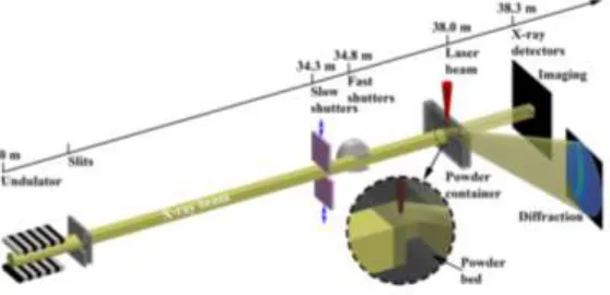
8 Studies involved using synchrotron X-ray to image the condition of a laser systems melt
pool was done by Zhao and others (Zhao et al., 2017). Utilizing a high-speed, hard X-ray from a
photon source (shown in Figure 2.4). A single melt track of powder from the side while a laser
source on top of the powder performs the scan, with the diffraction and imaging detector place
downstream of the photon source. The formation process of the keyhole pore was observed deep
under the base metal and it has revealed that the closure of keyholes took less than 50µs, and that
the void generated deep under the surface was pinned by the advance solidification front in the
leading edge of the beam.
Figure 2.4. Schematic of the high-speed X-ray imaging and diffraction experiments on laser powder bed fusion process at the 32-ID-B beamline of the Advanced Photon Source (Zhao et al.,
2017)
Trap gas porosities in the EBM process are traces of gas left in the powder feedstock
during the atomization stage when they’re manufactured, which are very hard to eliminate due to
the rate of solidification. Methods such as suppressing the entrapment of atomization gas during
the powder making process would help to mitigate the amount of trapped gas but requires the use
of an alternate atomization mechanism, as the lower energy can avoid the “bag breakup and
9
2.1.2 Geometric Defects and Deformation
EBM manufactured parts may exhibit different types of dimensional and geometric deviations
from the nominal model. Mousa (2016) investigated the curling phenomenon, i.e. a combination
of shrinking and warping that yields a curved profile of down-facing surfaces intended to be flat.
Curling is usually associated with an uneven shrinkage between the top and the bottom of the
part. Warping is due to the thermal stress formed by the rapid solidification during AM process,
as the temperature gradient leads to the differences in thermal expansion within the formed parts
(Vo et al. 2018). Another kind of geometrical distortion observed and investigated by different authors is rough surfaces of as-formed layers (Yasa et al, 2009, Kleszczynski et al, 2012). This combine with the curling may interfere with powder spreading and bed uniformity is successive
layers. Another potential geometric defect in EBM is that the beam deflection system may be
affected by external magnetic influences, which can change the beam path and shape of the beam,
resulting in defected geometrical part defects. This type of can be resolved by isolating the
machine from nearby electrical and magnetic sources.
2.1.3 Microstructure and Anisotropy
A common microstructure feature observed in metal AM parts is columnar grain morphology
(Kok et al, 2018). These columnar grains are typically aligned parallel to the build direction and
caused by the solidification condition common in metal AM. (shown in Figure 2.5). Re-melting of
previous layers during the material deposition process would create epitaxial columnar grain
growth while provide sufficient thermal gradient within the melt pool, which would prevent
10 of the anisotropy and heterogeneity in material properties. Meanwhile literatures have shown that
altering the scan strategy across layers is able to control the formation of either equiaxed or
columnar grains (Dehoff et al., 2015, Helmer et al., 2016), to differences in the overall direction of the thermal gradient (Ishimoto et al., 2016, Thijs et al., 2013), as well as the use of in-situ printed heat sink to manipulate it (Jamshidinia, 2015).
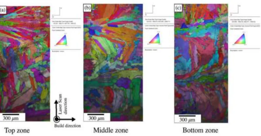
Figure 2.5. Inverse pole figures of samples fabricated using the line scan mode (a)
Corresponds to the top zone of the build (b) corresponds to the middle zone and (c) corresponds
11
2.2 In-situ Sensing
Mani et al. (2015) at NIST define the variables that can dictate the outcome of the AM process as “process signatures”. These are the dynamic characteristics of the powder heating, melting, and
solidification processes as they occur during the build which can be categorized into observable
and derived signatures. The former can be observed and measured during the process by using in
situ sensing devices while the latter can be determined through analytical models or simulations.
The following review is focused on the in situ sensing and monitoring approaches used in the
electron beam system; Laser systems will not be discussed in detail here but may share some
technologies with additions of active sensing methods due to the atmospheric environment.
2.2.1 Visible Wavelength Imaging
Visible wavelength imaging is currently being implemented widely for the powder spreading
condition of EBM systems. ARCAM uses a preoperatory camera system to image post rake and
melt at each layer for quality control during building. This information can be correlated with
microstructure and defects in post-processing analysis, however, is not used for closed loop
control (ref ref ref). Other studies have used high-speed camera to validate the beam velocity to
calculate the solidification time of the microstructure (Zhang et al., 2018). Laser systems allow for a more intricate camera system for process monitoring. And the earliest in-situ monitoring
studies were published by several groups (Kruth et al., 2007 and Doubenskaia et al.,2010). These researches use a coaxially mounted camera pyrometer to investigate the melt pool shape and
temperature. Further coaxial monitoring was investigated by Lane, Grantham, and others at NIST
12 direction. Images processed from the data produced has a resolution down to 1.67µm, which is
suitable to detect most defects produced by current metal AM systems (Lane et al., 2017). To monitor the melt pool Craeghs et al. (2012) experimented with an integrated optical setup that allows the position of the laser relative to the powder bed to be logged in tandem with
the melt pool data. The data from the individual melt pool were processed into a greyscale map of
the part, to resolved part overheating, porosity, and “balling” of the melt pool. Many reports have
used high-speed imaging in metal AM to measure a verity of melt pool phenomena. Furomoto et al. (2012) experiment with an in-line melt monitoring system using a high-speed camera
assembled vertically above the powder bed to observe the condition of the metal powder during
irradiation, illuminated by a metal halide lamp. A similar setup has been used to observe the melt
pool formation and spatters in several (Gunenthiram et al., 2017, Ly et al., 2017, Khairallah et al., 2016, and Haehnel and Dade, 2008), which may lead to defects in metal AM parts. These include
recoil pressure build-up by the metal vaper within the melt pool, Marangoni effect that causes
convection flow within the melt pool, shown in Figure 2.2. (b), and vaper jet entrainment of
microparticles, where the hot melt pool produces an argon flow towards the incoming laser and
the surrounding cooler environment.
The produced ejecta presents a problem as the ejected partials re-solidifies and sometimes
reincorporated into the melt pool and had been shown to reduce the tensile strength of the
produced parts (Liu et al., 2015). The usage of high-speed imaging to monitor the AM process had demonstrated effectiveness on validating or observe part quality, although the process was
mostly manual and the requirement of a large amount of hardware to process the video data
13
2.2.2 Thermal Imaging
Infrared system focuses on obtaining electromagnetic radiation with a wavelength of 700nm to
1mm, which uses emissivity data of a given surface to determine temperature estimations and
thermal gradients. Schwerdfeger et al. (2012) experimented with near-IR imaging during the
EBM process by perform layer snapshots of a post-melt surface and others use it for examining
surface temperature information to predict volume experience heat flux due to build geometry,
while using it to control material characteristic and part deformation (Paul et al., 2014).
Correlations between thermographic IR images and build microstructures were made and that by
using thermal cycles and results of computational thermodynamic models that calculate the
solidification of the microstructures and the kinetics of precipitation, process parameters for EBM
system can be guided (Sames et al., 2014).
The IR image taken in between layers can be utilized for in-situ control of the machine, as
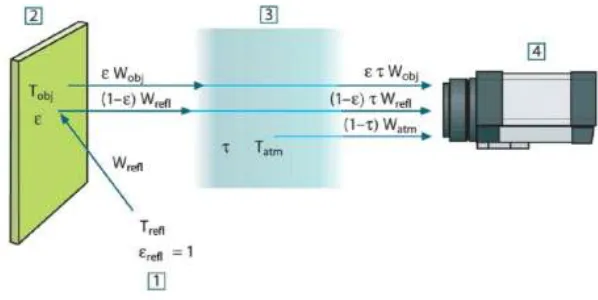
done by Mireles et al., (2015) using a FLIR infrared camera proposed by Rodriguez and others (Rodriguez et al., 2012). The IR camera measures the radiation emitted from the object as
𝜀𝜏𝑊𝑜𝑏𝑗, the reflected radiation from ambient sources (1 − 𝜀)𝜏𝑊𝑟𝑒𝑓𝑙, and emission from the
atmosphere (1 − 𝜏)𝑊𝑎𝑡𝑚, shown in Figure 2.3. The total received radiation power can be
expressed in terms of the total measured camera output voltage 𝑈𝑡𝑜𝑡 (Rodriguez et al., 2012).
𝑈𝑡𝑜𝑡 = 𝜀𝜏𝑈𝑜𝑏𝑗+ (1 − 𝜀)𝜏𝑈𝑟𝑒𝑓𝑙+ (1 − 𝜏)𝑈𝑎𝑡𝑚 (1)
Figure 2.6 shows three different sources of energy, W that the IR camera receives
translates to a camera output voltage U. The signal U is obtained by multiplying a constant C (by
14 emissivity of the object and τ is the transmittance of the atmosphere. Mireles et al., (2015)
developed LabVIEW code to automate the image acquisition and control of the ARCAM software
to adjust beam parameters between layers. This study reported success in detecting pre-generated
porosities within the build and producing graded microstructure within a single part. Rodriguez et al. (2012) also reported emissivity difference between powder and solids, since powder material exhibits a much higher emissivity, which contributes to most of the received reflected sources by
the IR camera. The transient temperature decay factor makes the IR measurement differ from the
actual temperature, therefore by recording in IR videos, changes between powder and solids can
be observed, although the accurate temperature is difficult to resolve using IR alone.
Figure 2.6. A schematic representation of the general thermographic measurement situation. 1:
Surroundings, 2: Object, 3: Atmosphere, 4: Camera. Courtesy: FLIR Systems AB. (Pandet et al. 2013)
Despite the limitations in accurate temperature acquisition, high-speed thermal imaging
had been successful in studies aim to validate simulations on the thermal condition of the AM
process. Lee et al. (2018) had successfully demonstrated microstructure control by using different
15 as input for the thermal model to target specific thermal gradient (G) and solidification rate (R).
Different scan strategies and beam pattern were used to target columnar to equiaxed transitions in
IN718, as the heating of the neighboring region effetely lower the G and appropriate spacing
between spots increases R. The pattern being tested is the ghost beam strategy which uses a
primary beam to perform the melt and a following secondary to reheat the as-formed melt pool.
Jamshidinia and Kovacevic (2015) employed a closed-loop monitoring system had been
demonstrated capable of detecting heat accumulation due to surface roughness, as these defects
can be mitigated with powder dosage control, beam current intensity, and beam scan strategies.
For laser systems is well suited for pyrometer measurement, as the direct contact of the
object of interest and the device is not required. The studies done by Pavlov et al. (2010) used a
bi-color pyrometer that was integrated into the laser machine’s optical scanning system and found
that the signal feedback from the pyrometer can be sensible enough for further in-situ control
integration. Cordero et al. (2017b) demonstrated that pyrometers are capable of obtaining more detailed, localized temperature data from the build platform, and suggesting that while it could be
a good substation for thermocouples, it is not as versatile as IR cameras.
Another complicating factor in performing in-situ EBM monitoring using external devices
is the requirement of a clear line of sight are subject to metallization of the viewing port caused
by evaporation and condensation of metal from the melt pool during the process. To mitigate the
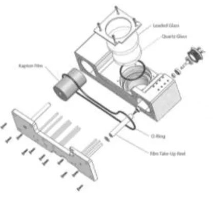
situation apparatus such as Kapton films (shown in Figure 2.7.). It would often utilize a motor
driven Kapton film roll (Dinwiddie et al., 2013) that acts as a sacrificial barrier against metallization. Another solution is to use mirror protected window, where a mirror directs the
field-of-view of the IR camera away from the build chamber to avoid a direct line-of-sight of the
16 friction and vacuum, which could cause the film to melt under high temperature, plus
metallization of the Kapton film changes the transmissivity of the material which reduces the
amount of infrared radiation reaching the IR camera, resulting in a lower approximation of the
calibrated temperature (Raplee et al., 2017) .
Figure 2.7. Exploded schematic view of the Kapton Film based shutterless window protection
system. (Dinwiddie et al., 2013)
2.3 Introduction to Electron Imaging
Electron monitoring was first proposed to be a method of tracking the seams between welds in EB
welding (Graham and Wingfield, 1965). These researchers envisioned a real time detector that
assured the welding beam accurately track the seam of the weld piece. The design was an in-line
detector comprised of an isolated metal disk that was symmetrical with the beam port and
surrounded by a Faraday shield. It had also proposed to synchronize the electron signal with the
17 the condition of the workpiece and give examples of using a simple metal plate to collect all the
types of scattered electrons. It also indicates the detection of the secondary and backscattered
electron coming from the melt pool is a possible way extract information from the different layers
of molten material.
The principle of this type of detection is similar to the gaseous secondary electron detector
(GSED) used in environmental scanning electron microscopes (ESEM).Secondary and BSE
emissions from the sample complete a biased circuit connected to a metal plate located on top of
the chamber, where the detected electron produce current (Knowles and Smith, 1999). The actual
condition of the secondary electron (SE) and backscattered electron (BSE) emission inside the
EBM system had not been studied until recently, it has been shown that it’s possible to take
geometric measure of the material and even see the condition of the melt pool (Arnold et al., 2018) with electronic imaging, which would be discuses later.
2.3.1 Background on SE/BSE
Electron imaging in general is utilizing an electron source (electron gun) to deposit a stream of
electrons (incident beam) to hit the target of interest, as the beam hits the target a plethora of
event occurs to generate various signals (shown in Figure 2.8). Secondary electrons (SE) are
generated from inelastic scattering of electron s originated from the target material. Scanning
electron microscope (SEM) are signals generated from the entrance side, and only at a depth of
0.5nm to 1.5nm where the secondary electrons are generated can escape to surface (Seiler, 1983).
SE can also be produced by the BSE and its contribution to the SE yield was investigated by
18 𝛿 = 𝛿𝑃𝐸+ 𝜂𝛿𝐵𝑆𝐸 = 𝛿𝑃𝐸(1 + 𝛽𝜂) (3)
𝛿𝑃𝐸 is the number of SE emitted for every primary electron (originate from the incident
beam), 𝛿𝐵𝑆𝐸 is the number of SE emitted per given BSE, where as 𝛽 = 𝛿𝐵𝑆𝐸/𝛿𝑃𝐸. Due to the lower average emergence angle of the BSE, it’s more favorable for the excitation of SE than the
incident beam itself, 𝛽 is always > 1, and according to Bronshtein and Dolinin (1968) 𝛽 decrease as the angle of the incident beam increases.
Backscattered electrons (BSE) are the electrons originated from the sources that got
diverted by the atoms inside the target, underwent a series of elastic scattering event.
𝜂 = 𝐼𝑟
𝐼0 (4)
Equation 4 describes the BSE coefficient 𝜂, and denotes the fraction of backscattered electrons to the incident beam electron (Equation 3), 𝐼𝑟 is the current of electrons backscattered into angles > 90 °, and 𝐼0 is the current of the incident electron beam. The 𝜂 coefficient increases as the target’s atomic number increases; hence BSE can be used for compositional imaging
(Napchan, 2001). Backscattered electron has a much more angular distribution compare to SE,
and are more energetic it easier to detect. As BSE scatters between atoms within the target it will
produce SE signals and would add to the total SE yield, and by subtracting the BSE signal it’s
possible to suppress the less localize material information (Niedrig, 1978).
Transmission electrons are the original electron beam that passes through the target. This,
along with the SE generated from the back side of the target, are the signal source for equipment
such as transmission electron microscope.
Other species include Auger electrons, characterized by the Auger effect, which are the
19 removed by the incident beam. During these interactions X-rays and cathodoluminescence are
emitted from the surfaces a will, the former can be used as energy dispersive X-ray spectroscopy
(EDS) and the latter as optical image of the target with color. Electron beam induced current
(EBIC) are the electrons originated from the incident beam that was absorbed by the target, it is
most commonly used as a way to probe subsurface p-n junctions in semiconductors. (Goldstein,
2003)
Figure 2.8 Emission of various electrons and electromagnetic waves from the specimen.
2.3.2 Electron Detection Hardware
The most widely used SEM detector is the Everhart-Thornley (ET) detector (Robinson, 1973) that
utilizes a photomultiplier to amplify the faint trace of photon given off by the scintillator when it
was struck by an electron. A grid of metal mesh covers the tip of the scintillator is biased
20 modified version of ET detectors uses a dynamically bias range from -500V to +500V as the
negatively bias mash would repeal electrons at the lower energy level while the higher energy
ones like BSE would go through; this type of detector was later dedicated to SE detection as
others types were investigated due to its poor resolution (Kimoto and Hashimoto, 1968).
Originally, ET detectors were design only to detect SE, however, later modification uses different
biased voltage to detect both SE and BSE.
Solid-state detectors or p-n junction detectors are a piece of annular (Wolf and Everhart,
1969) semiconductor and sometimes are divided into four quadrants for directional accuracy, it’s
useful for some non-imaging applications, for example, these detectors are capable of topographic
and compositional contrast (Kimoto et al., 1966), or channeling contrast (Coates, 19670. While the annular solid-state detector was widely implemented, the low gain and slow frequency of
these detectors generally produce inferior results with a lower SNR (Robinson, 1980) compared
with ET type detectors.
Other detectors intend to subsequent detectors aim at better BSE detection by placing it
closer to the target and biased it to ground, thus excluding the SE signals (Cordero et al, 2017). Wells (1974) experiments with different ET detector placement and found that the takeoff angle
produce a better compositional image, whereas a low takeoff angle produces a better topographic
image. These findings were experimented in modern detector designs (shown in Figure 2.9).
Another type is the converted BSE detector which converts the incoming BSE signal into SE by
placing a negatively biased grid placed over the detector to divert the incoming BSE (Reimer and
Volbert, 1979), this type of detector is able to produce low SNR image even at low accelerating
21
Figure 2.9. Different types and configurations of BSE detectors. (Coates, 1967)
SEM has constrains on the types of specimen it can examine due to its vacuum chamber,
however, various technology advancements targeted at organic materials had aim to solve this
issue with chambers that can operate at low vacuum pressure. Variable pressure scanning electron
microscope (VPSEM) operates at a sample chamber pressure of 2 Torr, whereas environmental
scanning electron microscope (ESEM) aimed at a pressure of 50 Tor (Mohan et al., 2006). At this level of chamber pressure the mean free path for SE is down to a few µm, reducing the total
22 since it requires the detector parts to be biased to several thousand volts, which has the possibility
of flashing over to ground with the presence of low pressure gas. Danilatos (1983) overcame the
problem by using the gas within the chamber as a means of amplifying the electron signals, the
amplified SE signals are detected by a positively biased metallic ring or wire and then connected
to an electronic signal amplifier that’s grounded to the machine (Danilatos and Robinson, 1979).
This type of detector, also known as GSED, has demonstrated to produce similar quality SE
images to that of the ET detectors, this id due to the fact that SE exhibits the highest interaction
cross section amount with incident beam and BSE that are also populating the specimen chamber
(Farley and Shah, 1991). Danilatos (2012) continues to investigate the alternative of solid-state
detectors to abstaining the BS information from a gaseous environment, for it generally has a
lower SNR compared with scintillator device due to their detective quantum efficiency under
SEM configurations (Baumann and Reimer, 1981), and Oatley (1985)). In this case an yttrium
aluminum garnet single crystal as the scintillating device that situated in the same location for
solid-state detectors but does not require the bias element in traditional ET type scintillation
23
2.3.3 Electron Imaging in AM
In metal 3D printing, this electron monitoring technology is first implemented in the EBM system
by swapping the original ARCAM S12 gun assembly with an industrial electron beam wielding
gun with a build in BSE (Arnold et al., 2018). This work is the first to demonstrate in metal 3D printing, the potential of electron imaging technology and its advantages over optical imaging, as
the incandescence phenomena of the electron gun is negated (Wysocki et al., 2017).
Arnold et al. (2018) performed layer images during an extra procedure for each layer, after the melting of the powder, to investigate the porosity detection capability of the system. An article
was built with 165, 210, 255 and 300 W to artificially create lack of fusion porosity.
Subsequently, the article was X-ray CT scanned to verify the electron imaging result. In
comparison with CT images the BSE generated images are limited in terms of its special
resolution but had shown promising capability in porosity detection and had suggested using
off-axis electron detectors to obtain more information of the surface typology. Using the same setup,
the electron images had been used to verify the process window of Ti-6Al-4V (Pobe et al., 2019), suggesting it as a tool for future process parameter development.
Wong et al (2018 a,b,c) on the other hand, modified the heatshield of an ARCAM A1, using the principle of GSED in ESEM, illustrated in Figure 2.10, where a piece of metal was
utilized to pass the small current induced by the received electron to an amplifier, where the
output of that signal was being subtracted from the amplified signal of a noise plate, which was
another isolated piece of metal plate behind the detector plate. Such arrangement was aimed to
increase the SNR and shown to be affective in producing quality image of the target.
To initially test the setup Wong et al (2018 a,b,c) performed a low current scan of 1mA and the beam speed of 11800 mm/s was used to generate the scanned image of the standard A1
24 was also investigated. Samples was also heated up to 650°𝐶 to observe the detectors
performance with different temperature, with the electron beam coordination data obtained
from the gun XY deflection coil voltage control, and the intensity of the signals were populated
into the corresponding location as grayscale bitmap, and had point out in the author’s previous
work. The author’s subsequent research (Wong et al., 2019) concluded that the resolution for the experimental set up is limited to the beam size of the machine, hence a limitation to the
magnification of the image. The result of the experiment was examined with histogram-based
image quality factor Q, which represented the degree of separation between the two-pixel value
classes and found that the elevated temperature had little effect on the quality of the image. This
finding on the performance of the experimental imaging device along with the physics of the SE
emission, where the kinetic of the atom out weights the effect of temperature (Bruining, 1954),
further strengthen the possibility of an in-situ electron base monitoring device in EBM system.
25
2.4 Literature Summary
This review covers the current methods of monitoring and forms of data extraction for the
building environment of powder bed AM processes used in pass experiments, including the detail
of the setup, observed data and some of the results listed in literature. These monitoring methods
enables the studies of powder bed machine parameters, conditions of the melt pool created during
different processes, and for some experimental setups, the quality of the monitoring method itself.
Many of the studies conducted with the outlook of achieving in-situ process monitoring, meaning
having a real-time control parameter changes during the machines operation, while in most cases
reach the step of validating the monitoring system few complete the step of real-time parameter
change mid build.
Each methods of monitoring have the strength of its own and limitations, with optical and
thermal systems in general requires optical path the extract data from the build environment it is
less challenging in laser systems than in EBM systems. Many of the studies includes the thermal
information of the building environment for the fact that the meteorology of the material which
closely related to its applications, is dictate by the microstructure formed at different thermal
profile of the build environment. Other challenges of in-situ control of the machine with image
feedback is the amount of computing power and the time delay for image analysis, for example,
the high-speed camera image, or to deduce what parameter to change for certain hot spot detected
by inferred camera, and in most commercial solutions it’s difficult to manipulate the control
26
CHAPTER 3: Electron Monitoring of EBM System
3.1 Introduction
The EBM apparatus of the EBM system allows for the principle of BSE imaging to be
implemented as a means of a non-intrusive monitoring method, similar procedure was performed
in scanning electron microscopes (SEM) and electron beam welding machines (Wollenhaupt et al, 2014). In order to estimate the signal range of any electron event caused by the incident beam
Wells (1970) model of electron interaction was considered, where signals from the elastic,
inelastic electrons, and the transmitted electrons combines to be the incident beam’s intensity. As
the capability of layerwise electron monitoring in EBM being experimented by Arnold et al. (2018) it has been proven to be an effective way to detect the formation of post melt surface
porosity, yet the system implemented in the apparatus was a commercially available electron gun
with built-in BSD detector and supporting imaging software (Clauß, 2018); in order to perform
electron imaging with the gun system of the ARCAM machine additional data acquisition
interface and imaging software are needed, as well as additional scanning procedure performed by
the EBM machine. Electron signals originated from the current passing from the detector element
to the build platform is being measured by the voltage differential between a shunt resistor that is
in series with the detector (Williams, 1984), a current to voltage convertor circuit with the
measurement range of 0 to 20mA was choose to encumbers the operating current range of the
electron gun. This chapter will outline the process of designing the detector element, as well as
discuss the many experiments and hardware iterations that bench mark the capabilities and
27
3.2 Electron Signal Detection
To measure the signals off of the detector plate the necessary physics of the nature of the signal
must be understand in order to choose the correct hardware for the task. The electron interaction
in the EBM system is much more complex than an electron microscope or in EB-welding, as the
more energetic interaction of the EBM will create positively charged metallization and plasma
that would interact with the incident beam (Klassen, 2017).The phenomenon had been studied in
the field of vacuum deposition where the vaporization element would be created by a pulse laser
or an electron source. Two solutions to avoid the line-of-sight interaction are the bent-beam and
tilt-beam vacuum chamber design, which had be employed in the study of uranium atom beam
vapor velocity (Ohba et al., 2000). It was found that the electron impact excitation and ionization of the evaporated atoms are proportional to the amount of electron-atom collision and the
acceleration voltage of the electron source. As the material surface being further energized by the
incoming electrons it was found in the study of uranium charge partial species, that the total
thermionic emission would only exceed the combine signal of elastic and inelastic electron
interaction at a 2200K surface temperature (Nishio et al., 1992), and in the case for copper the temperature would exceed 2500K (Dowell, 2013).
Hence it is concluded that the main contributor to the signal during the scanning as well as
melting of the powder surface are electrons generated from the elastic and inelastic interaction of
the incident beam. Events such as spatter and target density will yield a change in electron signal
intensity, and in the case of smoking events where the charge build up could represent an inverse
of current flow, these could, theoretically, yield information concerning the condition of the melt
28
3.2.1 Theory
The signal generated form all the electron sources form the chamber of the EBM machine can be
simplified with the basic theory of electricity. Assuming a vacuum environment in Figure 3.1. (a),
the discharge (+) e supplied with v from point A move a distance of ds in an electric field E,
transferring a charge of dq from electro tip A to B under the potential of V under a time of dt.
The current i is dq/dt, or:
i = e E * v/V. (6) The same charge calculated in equation (6) can be connected even if the electrodes are not
connected, or connected through a very large resistor as in Figure 3.1. (b). The electrodes will be
connected through a resistor R and shunted by a resistor C equal to the distributed capacitance of
the system. The mode of charge flow through the system is determine by the time constant RC,
which would output a differential voltage signal Vs across the resistor. A simplified schematic of
the ESEM (or EBM) machine’s electron gun shown in Figure 3.1. (c) illustrated a negatively
biased gun anode at point G at –Vb, referenced at the cathode point A, upon discharge a beam of
electron to hit the target of interest C which would have induced a current to flow from the target
to E the chamber wall, F the electron detector plate, or D the base of the specimen, in multiple
forms of electrons.
(a) (b) (c)
29 The amount of current carried by all the interacted electrons would fallow Kirchhoff's
circuit laws, in which case the current passing through the secondary electron and backscattered
electron iSE and iBSE, along with the absorbed specimen current iSC would add up to equal the
incident beam current iB, shown as:
iSC = iB - iBSE - iSE. (7) The backscatter electron current will be iBSE = 𝜂 iB and the secondary electron current will
be iSE = 𝛿 iB (Wells, 1974), which would give us a range of what the electron signals inside the
EBM machine would look like. This analogy gives us a clear range of what equipment is best
suited for the current measurement, depended on the different backscattered and secondary yield
of the target material the signal produced inside an EBM will be in the range of 10 µA to 100 µA
in reference with the ground of the incident beam. Under the vacuumed environment of ARCAM
A2 with the preheat current of 25 mA, material such as copper would have a theoretical yield of
0.34. Reports of the backscattered coefficient and the secondary yield that exclude the
contribution of backscattered-induced secondary are found to be 0.25 and 0.1 for an acceleration
30
3.2.2 Monte Carlo simulation
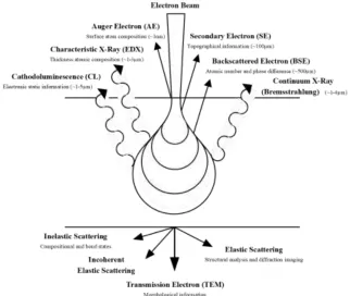
To understand the condition of the how the beam interacts with the target area interaction volume
simulation software CASINO v2 is used to determine the take-off angle and the information depth
of the apparatus (shown in Figure 3.2), the former is used for efficient detector placement whereas
the latter can indicate the information depth of the resulting signal. The program utilizes the
Monte Carlo method to estimate the possible pathways where electrons can travel within solid
materials, with the initial sets of boundaries defines the domain of possible inputs, the results will
be derive from the aggregated possible probabilities through deterministic computation on the
inputs (Kawrakow, 2000). Initial conditions of the program use the copper plate with a thickness
of 20mm, and the properties of the beam includes a 60kV acceleration voltage as well as a 200µm
beam diameter. The result indicates a detector placement that covers 0 to 55 degrees (referencing
the incoming beam) would be optimal for capturing the BSE signal which conforms to literature
data (Reimer and Riepenhausen, 1985), whereas the trajectory of SE is highly dependent on the
incident beam angle; with the operation range for the EBM system the SE to have a high take-off
angle of 30 degrees at low acceleration voltage, while converging toward 60 degrees at high
acceleration voltage (Carriere, 2018).
(a) (b)
31
3.3 Experimental Setup
3.3.1 Hardware Design and Iteration
The hardware setup, shown in Figure 3.3, for collecting the electron induced current signals
within an EBM machine was inspired by the design and research done by Wong et al. (2018) and Arnold et al (2018). For the initial validation of the image collecting capability of the detector a heatshield of the ARCAM A2 was electrically isolated with alumina oxide ceramic material,
connected to a transimpedance amplifier to convert into a voltage potential for the data acquisition
device for logging. Data for determining the precise location of where the beam was as well as
beam current, was obtained by tabbing into the machines control PLC. Scans of the surface of the
build was performed on the A2 custom small build tank while building with OFE copper; it was
happen to be what the modified machine was experimenting on at the time of the experiment, but
also happened to have the added benefit of a lower melting temperature compared with
Ti-6Al-V4 or other experimental material, provided a less harsh environment for the experiment, as well
as having a high conductive metallization on the heatshield detector that would still enables the
passage of the current signal.
32
3.3.2 Automatic Data Acquisition
The electron gun used in the ARCAM A2 is Rogowski-type tungsten filament electron gun that
uses the thermionic emission property of the material to generate the streams of electrons. As the
electrons exit the filament, they are being regulated by the biased electrode using the space-charge
limited regime (Carriere, 2018). This takes the control of beam current away from the
temperature-limited regime of the thermionic device, which can provide a faster respond time in
changing the beam current. The control bias voltage to the biased electrode, or grid cup, has a
feedback PLC voltage signal, which shows a polynomial trend with respect to the commanded
beam current from 0.1 mA to 20mA.
𝑉𝑔𝑟𝑖𝑑 = −0.1741𝐼𝑏+ 6.426 (7)
As 𝑉𝑔𝑟𝑖𝑑 is the grid cup control voltage and 𝐼𝑏 is the corresponding beam current output.
This has the potential for giving feedback to the electron imaging and control system, and at later
stage of the development it has been used as a triggering signal for the auto logging user interface.
In order to obtain the coordinates of each data point, what is essentially needed is where the beam
is pointing at in a given moment. The electron gun uses a series of magnetic coil to focus and
reshape the stream of electron, called condenser lenses, whose physics works in a similar fashion
as optical lances (Goldstain, 2003). Underneath the condenser lenses are the deflection coils with
dipole magnets who’s a magnetic field tangent to the beam to push the beam on two axes, with
the trajectory is change according to Equation (8):
sin(θ)=2.97*105 𝑙∗𝐵
33 As l is the length of the field and B is the magnetic field strength. The strength of the field can be change according to Ampere’s Law by the loops of winding current-carrying wires, define
by Equation (9):
B =𝜇0𝑁∗𝐼𝑎
𝑆 (9)
Where 𝜇0the permeability of free space, N is is the number of coils, 𝐼𝑎 is the current waveform created by the signal amplifier and S is the pole piece spacing. As l is significantly
larger than the distance from the center of the deflection system to the target, the distance for
which the beam would travel due to the change in field would be tangent to the center axis of the
beam. If assuming a small change in angle, as sin(𝜃) ≈ tan(𝜃), in this case equation (8) and (9) can be combined to yield a beam velocity of:
v=𝑑𝑥 𝑑𝑦=2.97*10 5𝜇 0 𝑁∗𝑙∗𝑧𝑑𝑒𝑓 √𝑉𝑐𝑐𝑆 ∗ 𝑑𝐵 𝑑𝐼𝑎 𝑑𝐼𝑎
𝑑𝑡 (10)
This shows that a deflection angle of less than 15 degrees would have a constant beam
velocity, exceeding it would require a fast, dynamic focusing system to offset the non-linear
acceleration at high deflection angles. With the working distance of 330mm and build surface of
200 x 200 mm in the standard build tank, and the build surface of 40 x 40 π mm for the small
build tank setup this effect can be omitted. The deflecting system has a mathematical model with
a stationary and a dynamic part. Stationary model is a particular solution of the dynamic
equations of the electrons when the electric and magnetic field distribution is known (Oltean and
Abrudean, 2008). The relation between the deflection distance on a linear axis and the deflection
34 𝑥𝑑𝑒𝑓𝑙 ≈ √
𝑒0 2∗𝑚𝑒∗
𝐾𝑏∗𝜇0∗𝑑𝑑𝑒𝑓𝑙∗𝑙𝑏
𝑎∗√𝑈𝑎𝑐𝑐 ∗ 𝑛 ∗ 𝑖𝑥𝑑𝑒𝑓𝑙 (11)
𝑑𝑑𝑒𝑓𝑙 is the distance from the coil to the material surface, 𝑙𝑏 the coil length and 𝑎 is the
coil dispersion constant. The dynamic model of the deflecting system on the linear axis is given
by:
𝐿𝑠𝑑𝑖𝑥𝑑𝑒𝑓𝑙
𝑑𝑡 + 𝑅𝑠𝑖𝑥𝑑𝑒𝑓𝑙(𝑡) = 𝑢𝑥𝑑𝑒𝑓𝑙(𝑡) (12)
The control system of the ARCAM uses PLC signal to control the deflection hardware,
which is also outputs a linear signal to the deflection coils current input controller. Preliminary
experiment on the PLC signal output shows a linear relationship between the previously
mentioned control signals and the distance traveled on the build plate, showing a possibility of
using it as a coordinate system for the graphical representation of the electron signals. During the
hardware developing stage both the PLC control signal and the deflection card control signal had
been experimented with and as the resulted image shown in Figure 3.6. The former is clearly the
superior option in terms of spatial resolution. Noted that the location of individual pixels is
resulted from the interpolation of the signals from the control side, events such as beam defocus
due to charge build-up of the surface in a smoke event, beam deflection oscillation due to the
instability of the deflection system’s power supply (Trushnikov, 2013), or external magnetic field
interference.
In order to test the capability of electron monitoring during melt a series of experiments
were set up to coordinate the BSE and SE intensity to the melt pool condition. The data collected
form the melt pool is closely related to the incident beam current, while other factors could also
contribute to the change in intensity of the combined BSE and SE signal. To identify possible
35 different parameters was performed, with the first being tracks raging from 3mA to 20mA beam
current with the same beam speed, and the second being tracks with a matching PV of 1000 in the
same current range.
Process monitoring was also performed during the production of copper cavities for
x-band radar applications, for the build duration of 8 hours the automatic logging LabVIEW
software was implied to distinguish the start of the preheat period and the end of the melting stage
from the amount of the voltage going in the grid cup control. Details of the LabVIEW code can be
found in Appendix A.
(a) (b) (c)
36 With two detector plate placed in line of the incident beam the signals from each cam be
combine or subtracted to create compositional or topographical image of the surface (shown in
Figure 3.5). The last iteration of the detector design comprised of copper signal plates mounted on
a copper ring block, all components are electrically isolated from each other. In compositional
mode, signals from the two plate are joined by a BNC interface and fed to the current to voltage
convertor, and passed to an X1 gain differential amplifier to subtract from the noise signals
originated from the copper ring block. In topographic mode the signals from the two plates are
subtracted from each other by a differential amplifier without the input from the noise plate, as
any inherent noise signal will be cancel out during the operation. The following experiments are
conducted with topographic mode intended to capture any potential melt pool characteristics at a
higher SNR, and for the operation range of the beam current a 1KΩ shunt resistor was used for
the current sensing circuit.
38
3.4 Result and Discussion
3.4.1 Melt Pool Characteristics form the BSE Signal
Figure 3.7 shows the comparison in electron signal intensity in the range of 17mA to 20mA, of
varying speed to maintain constant PV, and constant speed. While the different melt pool
formation did not reflect on the intensity of the current received by the detector, constant speed of
the beam represents higher energy input to the surface of the material did create a greater amount
of spatter, which give off 25% more noise compared with a constant PV beam.
Figure 3.7. (a) Current 3mA to 20mA, constant PV of 1000. (b) Constant speed.
The current imaging technique is unable to distinguish the different size of the melt pool
do to the correlation between deflection coil data and the electron signal, for each signal point
represents a combination of any point of contact to the part surface and the incident beam’s skirt
radius of 382 µm (Wong et al., 2019), and each interaction event would occur between the surface to depth of the backscattered electron escape volume of around 6 µm. Since the resolution of each
signal point around 300 µm, other melt strategies and signal analysis methods are needed in order
39
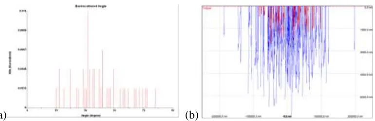
3.4.2 EBM Build Monitoring
Figure 3.8 (a) shows the current intensity of the electron signal during the melting of a layer. The
pattern shown on the surface is theorized to be the melt direction of the previous layer, and with a
line offset of 0.13 mm the beam is calculated to have remelted 50 % of the previously formed
melt track. A post melt layer scan using a beam current of 1 mA, a beam speed of 10000 mm/s
and a line offset of 0.1 mm, reveals a surface roughness condition after the melting process, where
the lower intensity region of the melted edge indicates curling. This scan also confirms that the
lower density powder layer would yield a lower signal intensity, which would be useful in
detecting spreadability issue, shown in Figure 3.8 (c). This procedure would take multiple scan to
be able to collect the amount of data needed to construct an image, and for the current parameter
set it would take an extra 20 second.
40 Figure 3.8. (b) A surface scan after a melt is completed
41 Figure 3.9 shows a stacked rendering of 271 continuous layers. Image processing was
performed in ImageJ, using the image stack functionality with interpolation. The cross section
reveals the porous overhang region caused by the increase in beam velocity, as well as lack of
fusion which shows up as dark spots within the cavity structure. Space within the inner cavities
were also rendered with grayscale color due noise signals accumulated during the acceleration of
the beam, thus it this should not be perceive as an indication of the density difference between the
solid part and the powder bed.
42
3.4.3 In-situ Melt pool Characterization
Figure 3.10 (a) shows the topographic surface of the melted powder layer in terms of electron
signal intensities, which was created through mesh generation of neighboring electron intensities
as the z height of the 3D surfaces. The topographical features captures by the electron interaction
produces significant contrast in the processed image, which can be conform by micro CT and
confocal optical images (Figure 3.10 (b) and Figure 3.10 (c)). The electron signal dropped at
locations where gas pockets are formed, as shown in Figure 3.11. This structure was observed
with high-speed camera, to originate from the out gassing of water vapor formed from electron
beam impact. As the vapor explosive escape the as formed melt pool front it would expand both
upward and downwards, where the former was captures as an outburst of material and the latter
expanded into the powder bed to form the pocket. With the melt pool front formed ahead of the
point of beam, such pocket geometry would also trap the scattered electrons and prevent them
from reaching the detector, hence the drop of overall signal. After the beam passes the as formed
pocket molten material would colipase and sometimes covered the pocket surface, much like the
formation of keyhole porosity.
44
3.5 Conclusion
With the introduction of electron optics, comes with an entire new way of studying the melt pool
condition of the EBM system. Signals from melt pool created from a higher power input create
spatters that reflects in higher SNR, this would theoretically happened if the incoming beam
encounters the powder material before it reaches the build plate. In this case the single ejecta
would be electrically isolated with the rest of the machine and during the interaction of an
incident electron, where the only path to neutral for the BSE or SE created during the process is
the detector plate. The extend of the exact ratio of the current that can be conducted through this
method although cannot be determine through the current experimental setup, should not exceed
the backscattered coefficient of the material multiplies the sensitivity of the detector. During the
melting stage of a build the spatter of material is less violent as the 40µm layer would sometimes
only contain a signal layer of powder, hence the capability of sublayer porosity sensing ability
over thick powder layer would not be applicable on a production build.
On the other hand, smoking events were also observed during the experiment and after
examining the electron signals it was discovered that during the suspected even time frame three
consecutive instances of negative current flow occurred after a quick buildup of charge, meaning
a current passing from ground to the detector. The inverse of current flow is the result from the
buildup and subsequent release of charge in the powder bed, and as describe in the study done by
Cordero (2017) that it can be treated as a capacitor. With the grounded detector system it can only
be speculate that at the point of the electron repulsion occurred on the individual powder partials
electric charge is also being carried away from the plate, into the surrounding chamber
45
CHAPTER 4: In-Situ Scanning Electron and Process Data Monitoring in the Electron Beam Melting Process
1. Introduction
Electron layer monitoring of the EBM process had become the focus of a good deal of
research recently due to advantages compared with optical monitoring methods, such as the lack of
incandescence influences occurred in near infrared optics due to the nature of the hardware (Wong
et al., 2018a,b [1] [2] ). The electron gun of the EBM system allows for the principle of electron
imaging to be implemented as a means of a non-intrusive monitoring method, similar procedure was
performed in scanning electron microscopes (SEM) and electron beam welding machines
(Wollenhaupt et al, 2014 [3]). Using the difference backscattered coefficient and secondary yield created by the seams of the weld piece, electron monitoring had been implemented in the feeding back
control system of the EB welding process as a seam detection system. As the capability of layerwise
electron monitoring in EBM being experimented by Arnold et al. (2018) [4] and Pobel et al. (2019) [5], using a commercially available electron gun (manufactured by pro-beam) with built- in BSD
detector integrated into an ARCAM A2 machine. It has been proven to be an effective way to detect
the formation of post melt surface porosity, yet requires additional scanning procedure performed by
the EBM machine. Wong et al. (2018 b) [2], on the other hand, electrically isolated the heat shield element within the build chamber and turning it into a detector. The modified heat shield technique
requires the minimal amount of modification to the original EBM machine, and has been tested for
using a beam current of 1mA and the beam speed of 11800mm/s to generate a surface scan image
ranging from room temperature to the 650C (Wong et al., 2019 a) [6], and has been tested to have a z
height resolution of 0.35 mm (Wong et al. 2019b) [7].