Energy Efficient Multiplier Design Using
Multi-Gate MOSFETs
Y.E. Vasanth Kumar1, A. Nandini2, B. Hyndhavi3
Assistant Professor, Department of Electronics and Communication Engineering, Wellfare Institute of Science,
Technology and Management, Visakhapatnam, Andhra Pradesh, India1.
B.E. Student, Department of Electronics and Communication Engineering, Wellfare Institute of Science, Technology
and Management, Visakhapatnam, Andhra Pradesh, India2,3.
ABSTRACT: This paper scrutinizesa low power method required to employ a high speed and high performance multiplier. The designs are structured using tri-gate MOSFET’s. To achieve low power and high speed, sleepy keeper technique is exploited to the multiplication process. Despite that, 10T full adder is employed to enhance the performance of addition process for the system. The system has been premeditated efficiently for 4-bit Braun multiplier using Tanner EDA.
KEYWORDS:Low-power, Single-gate MOSFET, Double-Gate MOSFET, Tri-Gate MOSFET, Sleepy Keeper, Full-Adder, Braun Multiplier.
I. INTRODUCTION
Over the past few decades, low power approaches has steadily geared up the design concerns for low power and high speed digital VLSI circuits to pioneer new techniques in the semiconductor world [1, 2].Moore’s law proves that the constraint of the transistors for designing VLSI circuits doubles every two years. Thus the transistor count is a significant concern that largely influences the design intricacy of many functional units such as multiplier and arithmetic logic unit (ALU). The multiplier plays a significant role in digital computations such as arithmetic operations in digital signal processor-DSP applications. Advances in VLSI design focuses primarily on low power and high speed multipliers in processor designs [1]. Taking these constraints into consideration, the design of low power multiplier is of great interest where AND gate and Full adder circuits are employed [3-5].In previous literatures single gate and double gate 10T full adder circuits are used to design multiplier architectures, consuming more power. To reduce this power constraint and to achieve high speed, Triple-gate MOSFET full adders and AND gates are proposed and compared to conventional designs. Further these two proposed designs are implemented using sleepy keeper technique to achieve energy efficient and high speed multiplier architectures.
In this paper chapter 2 explains briefly about single gate and double gate MOSFET Full adder designs whereas chapter 3 explains about the proposed tri-gate MOSFET designs with low power sleepy keeper approach. Chapter 4 provides the comparative analysis between single-gate, double-gate and tri-gate approaches in terms of power, delay and power-delay product and concludes finally in chapter 5.
II. LITERATURE SURVEY
MOSFETs are widely used in designing and implementing low power digital circuits. To attain low power, transistor sizing is done. Despite this, scaling channel length below 50nm lead to undesirable downsides such as short channel (SC) effects, variation in threshold voltages (Vt), drain induced barrier leakage (DIBL)etc [3, 4]. To overcome these
this 4T XOR gates, there is an improvement in reducing area, offers high speed and low power [5, 6]. The 10T full adder cell using single gate MOSFET is shown in figure 1.
Fig 1 10T Single-gate full adder
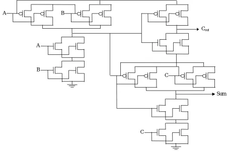
Similarly the 10T full adder with 4T double gate XOR is shown in figure 2 can greatly reduce the leakage power.
Fig 2 10T Double-gate full adder A
A
B
B
C
C
Cout
Sum A
A
B B
C C
Cout
Simulations are carried out to compare 10T double gate full adder with conventional single gate full adder. Experimental results are tabulated in table 1 and shows that the double gate achieves low power when compared to traditional designand the downside is that it offers low speed operations. To reduce this hindrance triple gate MOSFETs are exploited.
Table 1: Simulation results for 10Tsingle-gate and double-gate full adder circuits
Logic Power Delay PDP
Single gate 2.66E-21 9.9931n 2.65E-29
Double gate 2.62E-21 9.9965n 2.61E-29
III.PROPOSED METHOD
3.1 TRI-GATE MOSFET
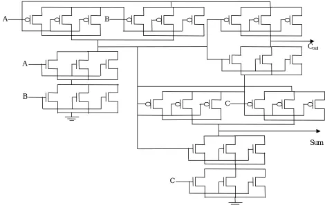
Tri-gate devices have gained so much attention as a result of their electrostatic properties. Compared to standard MOSFETs, tri-gate devices can perform at a much higher level due to geometries designed to maximize the control induced by additional gates. Basically we can design the 10T full adder using single gate, but there exists some threshold-voltage (vt) loss. So to reduce this voltage loss and to amplify the control over channel charges, the shorted
gates MOSFETs based full adder is used here, in which three transistors with their source and drain terminals tied together as shown in Figure 3. Even though the number of transistors are tripled compared to 10transistor logic, it will work efficiently with FinFET characteristics, and can greatly diminish the short channel effects.
Fig 3 10T Tri-gate full adder logic design A
A
B
B
Cout
C
C
3.2 MULTIPLIER
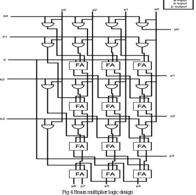
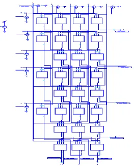
Multiplication is an important task in any arithmetic and logic unit (ALU) [1] and dominates the execution time of most DSP algorithms whose instruction time is determined by the multiplication time. Among different types of multipliers Braun multiplier, is a simple parallel multiplier generally called carry save multiplier (CSM) [7-9]. This parallel multiplier is used to perform the unsigned bit multiplication. The Braun multiplier shown in figure 4 makes of the array of array of AND gates and full adders [5-10]. In this paper the Braun multiplier is designed with the triple gate MOSFET based full adder, which is having less number of transistors compared to conventional one. So that we can achieve minimum area, low power and delay compared to previous designs.
Fig 4 Braun multiplier logic design
3.3 SLEEPY KEEPER TECHNIQUE
The downside with the conventional design is that the transistors are exploited only in their most efficient way namely PMOS and NMOS transistors connected to Vdd and Gnd respectively [6]. During sleep mode to maintain logic 1, the
mode, this NMOS transistor is the only source of VDD to the pull-up network since the sleep transistor is off. Similarly to maintain a value of logic 0 in sleep mode, given that the logic 0 has already been calculated, the sleepy keeper approach uses this output logic 0 and a PMOS transistor connected to GND to maintain output value equal to logic 0 [8, 10].
Fig 5 sleepy keeper block diagram
IV.EXPERIMENTAL RESULTS
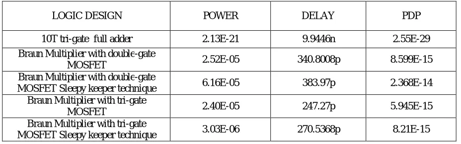
Simulations were carried out over tri-gate MOSFETS compared to single gate and double gate using tanner EDA in terms of power, delay and PDP. Evaluation result proved that the proposed design offer low power and high speed.The average powers of each case were measured and tabulated in table 2 and the propagation delay is measured for each of the multiplier architecture. Thus the efficiency of the system can be measured by using PDP.
Table 2: Simulation results for proposed Braun multiplier
LOGIC DESIGN POWER DELAY PDP
10T tri-gate full adder 2.13E-21 9.9446n 2.55E-29
Braun Multiplier with double-gate
MOSFET 2.52E-05 340.8008p 8.599E-15
Braun Multiplier with double-gate
MOSFET Sleepy keeper technique 6.16E-05 383.97p 2.368E-14
Braun Multiplier with tri-gate
MOSFET 2.40E-05 247.27p 5.945E-15
Braun Multiplier with tri-gate
MOSFET Sleepy keeper technique 3.03E-06 270.5368p 8.21E-15
The proposed sleepy keeper tri-gate braun multiplier and its corresponding waveforms are shown in figure 6 and 7 respectively.Where the braun multiplier is designed with high efficient 10T full adder with AND gate to reduce the leakage power with in the circuit design.The output waveforms are verfified accordingly for the inputs in the multiplication process from P0 to P7.
Pull-down Network Pull-down Network
IN OUT
S
Fig 6 Tri-gate Braun Multiplier using sleepy keeper technique
V. CONCLUSION
In this paper, we proposed a framework for designing high speed and low power multiplier using energy efficient full adder. A unique approach, tri-gate MOSFETs has been followed in the full adder design. This technique is combined with sleepy keeper approach to obtain the energy saving benefits with improved circuit performance in full adder design.The energy performance of the tri-gate full adder is compared with the conventional full adder designs. This proposed low power full adder cell is employed in the multiplier architecture.The performance of this design is analyzed with 4-bit Braun multipliers. The power results of the proposed multiplier designs are compared with the conventional logic designs. It is observed that the proposed multiplier circuits consume less power and offers high speed than the conventional designs.The proposed multiplier architecturehas been implemented and studied using Tanner EDA using 250nm technology and have shown great panorama for the development of power aware approaches. This design confirms the feasibility of multiplier in high speed and low power computing applications.
REFERENCES
[1] Kaushik Roy, S. C. Prasad,“Low power CMOS VLSI circuit design”, John Wiley and Sons Ltd, 2000.
[2] Sung-Mo Kang, Yusuf Leblebici, “CMOS digital IC analysis and design”, Second Edition, 1996.
[3] M. Suneela, P. Pushpalatha, “Design Of Area Efficient Low Power CMOS Full Adder Using 32nm Technology”, Proceedings of
AECE-IRAJ International Conference, 14th July 2013.
[4] H Bhagya Laxmi, T R Prasuna Barre, “Low Leakage and Power Saving 4-Bit BCD Adder”, International Journal Of Scientific Research
And Education, Volume 2, Issue 12, December-2014.
[5] Mohit Chopra, Navneet Gill, Harjeet Singh, “Performance Analysis of Full Adder Circuit using Double Gate MOSFET”, International
Journal of Computer Applications (0975 – 8887) Volume 129 – No.12, November2015.
[6] B. Srujana Sri, B. Saraswathi, G. Arun Kumar, A. Bhav Singh,“Design of Low Power 4-Bit Full Adder Using Sleepy Keeper Approach”,
IJRET-Volume: 01 Issue: 03 Nov-2012.
[7] P.S.H.S.Lakshmi, S.Rama Krishna, K.Chaitanya, “A Novel Approach for High Speed and Low Power 4-Bit Multiplier”, IOSR Journal of
VLSI and Signal Processing, Volume 1, Issue 3 (Nov. - Dec. 2012), PP 13-26.
[8] S. Kiruthika, R.Nirmal Kumar, Dr. S.Valarmathy, “ Comparative Analysis of 4-Bit Multipliers Using Low Power 8-Transistor Full Adder
Cells”, International Journal of Emerging Technology and Advanced Engineering, ISSN 2250-2459, ISO 9001:2008 Certified Journal, Volume 3, Issue 1, January 2013.
[9] Dayadi Lakshmaiah, Dr. M. V. Subramanyam, Dr. K. Satya Prasad, “Design of Low Power 4-Bit CMOS Braun Multiplier based
onThreshold Voltage Techniques”, By Global Journal of Researches in Engineering: Electrical and Electronics Engineering, Volume 14 Issue 9 Version 1.0 Year 2014.
[10] Jyoti Sankar Sahoo,Nirmal Kumar Rout, “Comparative Study of Different Low Power Designs of Braun Multiplier using Double Gate
MOSFET at 45nm Technology”, International Journal of Computer Applications (0975 – 8887) International Conference on Emergening Trends in Computing and Communication (ETCC 2015).
BIOGRAPHY
Y.E.Vasanth Kumar is an Assistant Professor in the Department of Electronics and Communication Engineering at Wellfare Institute of Science Technology and Management, Visakhapatnam, Andhra Pradesh. He obtained his B.Tech in the field of Electronics and Communication Engineering at Pydah Engineering College in 2007. M.Tech in Radar and Microwave Engineering at A.U.C.E (A), Andhra University in 2011. His area of specialization includes Radar, MWE, VLSI. He has supervised
projects at undergraduate levels.
Akula Nandini is a student persuing her B.Tech final year in department of ECE from Wellfare Institute of Science Technology and Management(WISTM), Visakhapatnam, Andhra Pradesh.. Her area of interest is low power VLSI design.