Performance Improvement and Size
Reduction Scheme over Circuits by Using
LUT/MUX Architecture
R. Pradeepa1, S.P. Senthil Kumar2
M.E. VLSI Design, Shanmuganathan Engineering College, Arasampatti, Pudukkottai-622507, India.
Assistant Professor, Department of ECE, Shanmuganathan Engineering College, Arasampatti,
Pudukkottai-622507, India.
ABSTRACT: For reducing the area and improving the performance of logical circuits, a combination of Look Up Table (LUT) with Multiplexer methodology is applied together. By implementing this kind of architecture a new MUX:LUT structure is designed, which works based on the number of comparators and logical circuits. This implementation is more suitable for both accounting for complex logic block and routing area while maintaining mapping depth. Interconnections are increasingly the dominant contributor to delay, area and energy consumption in Complementary Metal-Oxide Semiconductor (CMOS) digital circuits. The proposed implementation overcomes several limitations found in previous quaternary implementations published so far, such as the need for special features in the CMOS process or power-hungry current-mode cells. We have to use the 512bit quaternary Look Up Table for high level of operations in the FPGA. The proposed architecture of this paper will be planned to implemented and also analysis the output current, output voltage, area using Xilinx 14.3.
KEYWORDS: Field-Programmable Gate Array (FPGA), Hybrid Complex Logic Block, Multiplexer (MUX).
I. INTRODUCTION
Throughout the history of field-programmable gate arrays (FPGAs), lookup tables (LUTs) have been the primary logic element (LE) used to realize combinational logic. A K-input LUT is generic and very flexible—able to implement any K-input Boolean function. The use of LUTs simplifies technology mapping as the problem is reduced to a graph covering problem. However, an exponential area price is paid as larger LUTs are considered. The value of K between 4 and 6 is typically seen in industry and academia, and this range has been demonstrated to offer a good area/performance compromise. Recently, a number of other works have explored alternative FPGA LE architectures for performance improvement to close the large gap between FPGAs and application-specific integrated circuits (ASICs). In this system, we propose incorporating (some) hardened multiplexers (MUXs) in the FPGA logic blocks as a means of increasing silicon area efficiency and logic density.
In this system, we present a six-input LE based on a 4-to-1 MUX, MUX4, that can realize a subset of six-input Boolean logic functions, and a new hybrid complex logic block (CLB) that contains a mixture of MUX4s and 6-LUTs. The proposed MUX4s are small compared with a 6-LUT (15% of 6-LUT area), and can efficiently map all {2, 3}-input functions and some {4, 5, 6}-input functions. In addition, we explore fracturability of LEs—the ability to split the LEs into multiple smaller elements—in both LUTs and MUX4s to increase logic density. The ratio of LEs that should be LUTs versus MUX4s is also explored toward optimizing logic density for both nonfracturable and fracturable FPGA architectures. To facilitate the architecture exploration, we developed a CAD flow for mapping into the proposed hybrid CLBs, created using ABC and VPR, and describe technology mapping techniques that encourage the selection of logic functions that can be embedded into the MUX4 elements.
The main contributions in this system are as follows.
(a) Two hybrid CLB architectures (nonfracturable and fracturable) that contain a mixture of MUX4 LEs and the traditional LUTs yielding up to 8% area savings.
(b) Mapping techniques called NaturalMux and MuxMap targeted toward the hybrid CLB architecture that optimize for area, while preserving the original mapping depth.
(c) A full post-place-and-route architecture evaluation with VTR7, and CHStone benchmarks facilitated by LegUp-HLS, the Verilog-to-Routing project showing impact on both area and delay.
Compared with the preliminary publication, we have performed transistor level modeling of the MUX4 LE, further studied the fracturable architectures, and unified the open source tool-flow from C through LegUp-HLS to the VTR flow. Sparse crossbars have also been included in our CLBs, increasing modeling accuracy. The new transistor-level modeling of the MUX4 also provides more accurate results as compared with the previous work. Results have also been expanded with the inclusion of timing results as well as larger architectural ratio sweeps.
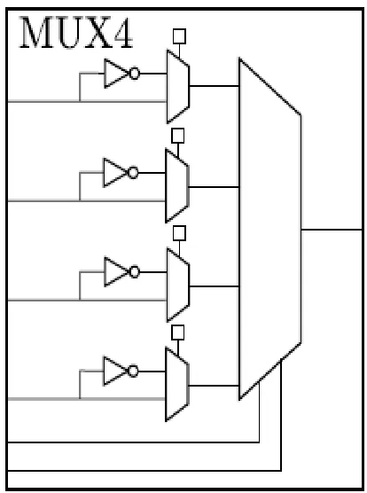
II. MUX4: 4-TO-1 MULTIPLEXER LOGIC ELEMENT
The MUX4 LE shown in Fig. 1 consists of a 4-to-1 MUX with optional inversion on its inputs that allow the realization of any {2, 3}-input function, some {4, 5}-input functions, and one 6-input function—a 4-to-1 MUX itself with optional inversion on the data inputs. A 4-to-1 MUX matches the input pin count of a 6-LUT, allowing for fair comparisons with respect to the connectivity and intra-cluster routing.
Naturally, any two-input Boolean function can be easily implemented in the MUX4: the two function inputs can be tied to the select lines and the truth table values (logic-0 or logic-1) can be routed to the data inputs accordingly. Or alternately, Shannon decomposition can be performed about one of the two variables—the variable can then feed a select input. The Shannon cofactors will contain at most one variable and can, therefore, be fed to the data inputs (the optional inversion may be needed).
For three-input functions; consider that Shannon decomposition about one variable produces cofactors with at most two variables. A second decomposition of the cofactors about one of their two remaining variables produces cofactors with at most one variable. Such single-variable cofactors can be fed to the data inputs (the optional inversion may be needed), with the decomposition variables feeding the select inputs. Likewise, functions of more than four inputs can be implemented in the MUX4 as long as Shannon decomposition with respect to any two inputs produce cofactors with at most one input. Observe that input inversion on each select input is omitted as this would only serve to permute the four MUX data inputs. While this could help routability within the CLB’s internal crossbar, additional inversions on the select inputs would not increase the number of Boolean functions that are able to map to the MUX4 LE.
Naturally, any two-input Boolean function can be easily implemented in the MUX4: the two function inputs can be tied to the select lines and the truth table values (logic-0 or logic-1) can be routed to the data inputs accordingly. Or alternately, Shannon decomposition can be performed about one of the two variables - the variable can then feed a select input. The Shannon cofactors will contain at most one variable and can, therefore, be fed to the data inputs (the optional inversion may be needed). For three-input functions; consider that Shannon decomposition about one variable produces cofactors with at most two variables.
A second decomposition of the cofactors about one of their two remaining variables produces cofactors with at most one variable. Such single-variable cofactors can be fed to the data inputs (the optional inversion may be needed), with the decomposition variables feeding the select inputs. Likewise, functions of more than four inputs can be implemented in the MUX4 as long as Shannon decomposition with respect to any two inputs produces cofactors with at most one input. Observe that input inversion on each select input is omitted as this would only serve to permute the four MUX data inputs. While this could help routability within the CLB’s internal crossbar, additional inversions on the select inputs would not increase the number of Boolean functions that are able to map to the MUX4 LE.
III. LOGIC ELEMENTS, FRACTURABILITY, AND MUX4-BASED VARIANTS
Two families of architectures were created: 1) without fracturable LEs and 2) with fracturable LEs. In this system, the fracturable LEs refer to an architectural element on which one or more logic functions can be optionally mapped. Nonfracturable LEs refer to an architectural element on which only one logic function is mapped.
This configuration allows this structure to map two independent (no shared inputs) three-input functions, while larger functions may be mapped dependent on the shared inputs between both functions. An architecture in which a 4-to-1 MUX (MUX4) is fractured into two smaller 2-to-1 MUXs was first considered. However, since a 2-to-1 MUX’s mapping flexibility is quite limited (can only map two-input functions and the three-input 2-to-1 MUX itself), little benefit was added compared with the overheads of making the MUX4 fracturable and poor area results were observed.
IV. EXISTING SYSTEM
In the existing system, it has six input LUTs based on 4X1 MUX in Boolean logic functions.
It has minimal efficiency on timing area and performances and also more delay occurs in the functions.
For Practical implementations, the cost requirement is comparatively high, but the expected output will be achieved, so that we have to bear the cost for accessing.
Disadvantages of Existing System
Delay rate is too high More Power Consumption Cost Expensive
V. PROPOSED METHODOLOGY
Two hybrid Complex Logic Block (CLB) architectures (non-fracturable and fracturable) that contain a mixture of MUX4 Logical Elements (LEs) and the traditional LUTs yielding more area savings.
Mapping techniques called NaturalMux and MuxMap targeted toward the hybrid CLB architecture that optimize for area, while preserving the original mapping depth.
A full post-place-and-route architecture evaluation with Verilog-to-Routing (VTR) benchmarks facilitated by LegUp-HLS, the Verilog-to-Routing project, showing impact on both area and delay.
Advantages of Proposed System
Delay is comparatively reduced.
Energy Consumption is reduces and low cost expensive in work. High Performance.
VI. LITERATURE SURVEY
To facilitate the development of future FPGA architectures and CAD tools -- both embedded programmable fabrics and pure-play FPGAs -- there is a need for a large scale, publicly available software suite that can synthesize circuits into easily-described hypothetical FPGA architectures. These circuits should be captured at the HDL level, or higher, and pass through logical and physical synthesis. Such a tool must provide detailed modelling of area, performance and energy to enable architecture exploration. As software flows themselves evolve to permit design capture at ever higher levels of abstraction, this downstream full-implementation flow will always be required.
This paper describes the current status and new release of an ongoing effort to create such a flow - the 'Verilog to Routing' (VTR) project, which is a broad collaboration of researchers. There are three core tools: ODIN II for Verilog Elaboration and front-end hard-block synthesis, ABC for logic synthesis, and VPR for physical synthesis and analysis. ODIN II now has a simulation capability to help verify that its output is correct, as well as specialized synthesis at the elaboration step for multipliers and memories. ABC is used to optimize the 'soft' logic of the FPGA. The VPR-based packing, placement and routing is now fully timing-driven (the previous release was not) and includes new capability to target complex logic blocks.
In addition we have added a set of four large benchmark circuits to a suite of previously-released Verilog HDL circuits. Finally, we illustrate the use of the new flow by using it to help architect a floating-point unit in an FPGA, and contrast it with a prior, much longer effort that was required to do the same thing.
To facilitate the development of future FPGA architectures and CAD tools -- both embedded programmable fabrics and pure-play FPGAs -- there is a need for a large scale, publicly available software suite that can synthesize circuits into easily-described hypothetical FPGA architectures. These circuits should be captured at the HDL level, or higher, and pass through logical and physical synthesis. Such a tool must provide detailed modelling of area, performance and energy to enable architecture exploration. As software flows themselves evolve to permit design capture at ever higher levels of abstraction, this downstream full-implementation flow will always be required.
In this system, we introduce a new open source high-level synthesis tool called LegUp that allows software techniques to be used for hardware design. LegUp accepts a standard C program as input and automatically compiles the program to a hybrid architecture containing an FPGA-based MIPS soft processor and custom hardware accelerators that communicate through a standard bus interface. Results show that the tool produces hardware solutions of comparable quality to a commercial high-level synthesis tool.
VII. EXPERIMENTAL RESULT
Fig.4. Schematic Design
Fig.6. Xilinx Design
VIII. CONCLUSION AND FUTURE SCOPE
Propose a new hybrid CLB architecture containing MUX and logical elements and shown techniques for efficiently mapping to these architectures. Implementation of LUT yields more power saving and area saving nature with cost benefits. The combination of MUX: LUT produces successful power consumption and size reductions schemas in single unit.
The proposed system guarantees the size and nature of the LUT MUX in more efficient manner, however in future this work is extended to interconnect many features, which are increasingly the dominant contributor to delay, area and energy consumption in CMOS digital circuits. This implementation overcomes several limitations found in previous implementations published so far, such as the need for special features in the CMOS process or power-hungry current-mode cells.
REFERENCES
[1] J. Rose et al., “The VTR project: Architecture and CAD for FPGAs from verilog to routing,” in Proc. ACM/SIGDA FPGA, 2012, pp. 77–86. [2] Y. Hara, H. Tomiyama, S. Honda, and H. Takada, “Proposal and quantitative analysis of the CHStone benchmark program suite for practical C-based high-level synthesis,” J. Inf. Process., vol. 17, pp. 242–254, Oct. 2009.
[5] J. Rose, R. Francis, D. Lewis, and P. Chow, “Architecture of fieldprogrammable gate arrays: The effect of logic block functionality on area efficiency,” IEEE J. Solid-State Circuits, vol. 25, no. 5, pp. 1217–1225, Oct. 1990.
[6] H. Parandeh-Afshar, H. Benbihi, D. Novo, and P. Ienne, “Rethinking FPGAs: Elude the flexibility excess of LUTs with and-inverter cones,” in Proc. ACM/SIGDA FPGA, 2012, pp. 119–128.
[7] J. Anderson and Q. Wang, “Improving logic density through synthesisinspired architecture,” in Proc. IEEE FPL, Aug./Sep. 2009, pp. 105–111. [8] J. Anderson and Q. Wang, “Area-efficient FPGA logic elements: rchitecture and synthesis,” in Proc. ASP DAC, 2011, pp. 369–375.
[9] J. Cong, H. Huang, and X. Yuan, “Technology mapping and architecture evalution for k/m-macrocell-based FPGAs,” ACM Trans. Design Autom. Electron. Syst., vol. 10, no. 1, pp. 3–23, Jan. 2005.
[10] Y. Hu, S. Das, S. Trimberger, and L. He, “Design, synthesis and evaluation of heterogeneous FPGA with mixed LUTs and macro-gates,” in Proc. IEEE ICCAD, Nov. 2007, pp. 188–193.
[11] I. Kuon and J. Rose, “Measuring the gap between FPGAs and ASICs,” IEEE Trans. Comput.-Aided Design Integr. Circuits Syst., vol. 26, no. 2, pp. 203–215, Feb. 2007.
[12] K. Karplus, “Amap: A technology mapper for selector-based fieldprogrammable gate arrays,” in Proc. 28th ACM/IEE DAC, Jun. 1991, pp. 244– 247.
[13] A. Mishchenko, S. Chatterjee, and R. Brayton, “DAG-aware AIG rewriting a fresh look at combinational logic synthesis,” in Proc. 43rd Annu. DAC, 2006, pp. 532–535.
[14] V. Betz and J. Rose, “VPR: A new packing, placement and routing tool for FPGA research,” in Proc. 7th Int. Workshop FPL, 1997, pp. 213– 222.
[15] S. A. Chin and J. H. Anderson, “A case for hardened multiplexers in FPGAs,” in Proc. FPT, Dec. 2013, pp. 42–49.
BIOGRAPHY