Power Amplifier
Linearisation Through
Second-Order Bias Injection
PhD Thesis
-? . r * 7 %
: :
4
^
a #
a » » . # *
May 2001
%T'
ProQuest Number: U642360
All rights reserved
INFORMATION TO ALL USERS
The quality of this reproduction is dependent upon the quality of the copy submitted.
In the unlikely event that the author did not send a complete manuscript and there are missing pages, these will be noted. Also, if material had to be removed,
a note will indicate the deletion.
uest.
ProQuest U642360
Published by ProQuest LLC(2015). Copyright of the Dissertation is held by the Author.
All rights reserved.
This work is protected against unauthorized copying under Title 17, United States Code. Microform Edition © ProQuest LLC.
ProQuest LLC
789 East Eisenhower Parkway P.O. Box 1346
Power Amplifier Linearisation Through PhD Thesis Second-Order Bias Iniection______________________ î r l l i l ï ______________________________________________
Abstract
This thesis describes the development o f a novel linearisation technique for use in
high-frequency power amplifiers. The need for linear power amplifiers is identified, and existing
linearisation schemes are outlined and appraised in terms o f their complexity, cost and
efficacy. It is shown that currently-available linearisation schemes tend to have an
effectiveness that is proportional to their complexity, and hence their cost o f implementation.
Analysis and simulation results are presented to illustrate the mechanism through which the
new linearisation technique reduces in-band distortion. The theoretical work is then verified
with experimental measurements, initially using two unmodulated carriers and a feedback
topology, and progressing to become a feedforward or ‘injection’ technique using four
unmodulated carriers. The agreement between the simulated and measured performance was
found to be excellent throughout.
The application o f the technique to modulated ‘real-world’ signals is then investigated, with
theoretical analysis, simulations and measured results presented to demonstrate the
applicability o f the technique to both single and multiple modulated-carrier input signals. It
is shown that Second-Order Bias Injection can typically provide 15-18dB o f in-band
distortion improvement, and that the technique has potential for use in next-generation (2G^
Power Amplifier Linearisation Through J PhD Thesis Second-Order Bias Iniection______________________ ____________________________________________________
Acknowledgements
There are numerous people without whom this work would not have been successful. I’d like
to begin by expressing sincere thanks to Dr Ahmad Khanifar for his support, guidance and
advice, especially during those periods o f difficulty with the work and in my personal life. I
am also indebted to Dr David Haigh and Dr Danny Webster at UCL for their generous
assistance in the nonlinear model extraction process, as well as for the advice and
constructive comments they have offered throughout the course o f this study.
Within Nokia, I would like to acknowledge the invaluable support and encouragement
provided by Dr Mahmoud Zadeh, and I would also like to thank Martin Goss and Richard
Kybett for lending me their time and experience.
Finally, in gratitude for their endless support and encouragement, this thesis is dedicated to
my parents.
Power Amplifier Linearisation Through PhD Thesis Second-Order Bias Iniection______________________ ï i t î i B ______________________________________________
Table of Contents
ABSTRACT
1
ACKNOWLEDGEMENTS
2
TABLE OF CONTENTS
3
1. INTRODUCTION
11
2. BACKGROUND
18
2.1 Nonlinearity 18
2.1.1 Strong and Weak Nonlinearity 19
2.1.2 Amplitude Distortion 21
2.1.3 Linear Distortion 27
2.1.4 Power Amplifier Intercept Points 28
2.1.5 Peak to Average Ratio, Back-Off and Efficiency 30
2.2 Linearisation Techniques 31
2.2.1 Power Back-Off 31
2.2.2 Feedforward 32
2.2.3 Predistortion 36
2.2.4 Negative Feedback 38
2.2.5 Active Feedback 39
2.2.6 Envelope Feedback 40
2.2.7 Polar-Loop Feedback 42
2.2.8 Cartesian Loop Feedback 43
2.2.9 ‘Linear Amplification Through Nonlinear Components’ (LING) 44 2.2.10 Second-Harmonic Feedback and ‘Interstage Second Harmonic Enhancement’ 44
2.2.11 Low-Frequency Feedback 47
2.3 Summary 50
3. SIMULATED AND PRACTICAL PROOF-OF-CONCEPT
51
3.1 Nonlinear Amplifier Model 52
3.1.1 2-D Maclaurin Series Description 52
3.2 Model Evaluation 57
3.2.1 S-Parameters 5 7
3.2.2 Input Power Sweep and Two-Tone Distortion Measurement 59
3.3 2-Tone Proof of Concept 62
3.3.1 Simulation o f Low-Frequency Feedback 62
3.3.2 Feedback Phase and Amplitude Sweeping 64
3.3.3 Simulated Power Dependence 68
3.4 Experimental Verification 69
3.4.1 Linearisation Through ‘ Low-Frequency Injection’ 70
Power Amplifier Linearisation Through
Second-Order Bias Iniection_________
A
PhD Thesis
3,4.3 Two-Tone Power Sweep 3.5 Summary
74 76
4.
MULTI-TONE INPUT SIGNALS
4.1 M ulti-Tone Linearisation
4.1.1 Multi-Tone Analysis and Discussion 4.1.2 Feedback Implementation Issues 4.1.3 External Generation and Injection
4.2 Practical Verification of M ulti-Tone Linearisation 4.2.1 Design and Build o f Four-Tone Combiner 4.2.2 4-tone Test-Bench
4.3 Experim ental Work 4.3.1 Simple Inversion
4.3.2 Equalisation with Convolution
4.3.3 Equalisation by Discrete Fourier Transform 4.4 Summary
77
77 78 81 83 84 84 89 92 93 94 99 1065.
MODULATED CARRIERS
5.1 Analysis of Single-Carrier Linearisation with Digital Modulation
5.2 Simulation of Single-Carrier Linearisation with Digital Modulation
5.2.1 Idealised Envelope Simulation 5.2.2 Idealised DSP/RF Co-Simulation 5.2.3 Power Dependence
5.2.4 Simulated Phase and Amplitude Tolerance
5.3 Experimental Single-Carrier Linearisation with Digital Modulation
5.3.1 Single Carrier Implementation and Testing 5.3.2 Measured Power Dependence
5.3.3 Measured Amplitude Tolerance 5.3.4 EDGE Modulation and EVM
5.4 Analysis of Multi-Carrier Linearisation with Digital Modulation
5.5 Simulation of Multi-Carrier Linearisation with Digital Modulation
5.5.1 Idealised DSP/RF Cosimulation
5.6 Multiple Modulated Carrier Proof-of-Concept
5.6.1 Test-Bench and Implementation Issues 5.6.2 Linearisation with IF Injection Signal
5.6.3 Linearisation with IF and Baseband Composite Injection Signal 5.6.4 Linearisation with Offset Carrier Amplitudes
5.7 Summary
108
108 112 112 114 116 117 121 124 129 132 133 136 140 140 143 143 144 146 153 1546.
SUMMARY, FUTURE WORK AND CONCLUSIONS
6.1 Summary
6.2 Practical Implem entation Issues
155
155 156
Power Amplifier Linearisation Through
Second-Order Bias Iniection______________________ 6.2.1 Single-Carrier
6.2.2 Multicarrier
6.2.3 Integration with Other Techniques
6.3 Comparison with Other Linearisation Techniques
6.3.1 Analogue Predistortion 6.3.2 Digital Predistortion 6.3.3 Feedforward
6.4 Future Work
6.4.1 IC Prototyping
6.4.2 Integration with Other Techniques 6.4.3 Investigation o f Performance Limitations
6.5 Conclusions
PhD Thesis
156 158 159
161
161 162 164
165
165 165 165
166
APPENDIX A
MDS FLL351ME Nonlinear Model Implementation
APPENDIX B
Measured MRF281 Test Amplifier S-Parameters
APPENDIX C
1 6 8
168
1 69
169
171
1. Pseudo random bit-stream generator
2. Pulse-shaping
3. Single-carrier linearising signal generation
4. Two-carrier linearising signal generation
REFERENCES
171
171
173
174
Power Amplifier Linearisation Through
Second-Order Bias Iniection_________
iim"
PhD Thesis
Glossary
ACP(R) - Adjacent Channel Power (Ratio)
ADC - Analogue-to-Digital Converter
ADS - Advanced Design System
AGC - Automatic Gain-Control
ALCPR - Alternate Channel Power Ratio
AM - Amplitude Modulation
AM/AM - Amplitude-modulation to amplitude-modulation distortion
AM/PM - Amplitude-modulation to amplitude-modulation distortion
ARIB - Association o f Radio Industries and Broadcasting (ARIB)
ASIC - Application-Specific Integrated Circuit
AWG - Arbitrary Waveform Generator
HER - Bit Error Rate
BJT - Bipolar Junction Transistor
BTS - Base Transceiver Station
CAD - Computer-Aided Design
CDMA - Code Division Multiple Access
DAC - Digital-to-Analogue Converter
DAPD - Digitally-Adaptive Digital Predistortion
DFT - Discrete Fourier Transform
DSO - Digital Sampling Oscilloscope
DSP - Digital Signal Processing/Processor
DUT - Device Under Test
EDGE - Enhanced Data Rates for GSM Evolution
ETSI - European Telecommunications Standards Institute
EVM - Error Vector Magnitude
FDMA - Frequency Division Multiple Access
FFT - Fast Fourier Transform
GCP - Gain Compression Point
GMSK - Gaussian Minimum-Shift Keying
GSM - Global System for Mobile communications
IF - Intermediate Frequency
IMD - Intermodulation Distortion
IMD3 - Third-order Intermodulation Distortion
IP2 - Second-Order Intercept Point
IP3 - Third-Order Intercept Point
LDMOS - Laterally-Doped Metal-Oxide Semiconductor
LINC - Linear Amplification Through Nonlinear Components
LPA - Linear Power Amplifier
Power Amplifier Linearisation Through Second-Order Bias Iniection_________
PhD Thesis
LPF - Low-Pass Filter
LTI - Linear Time Invariant
PA - Power Amplifier
PM - Phase Modulation
MDS - Microwave Design System
MESFET - Metal-Semiconductor Field-Effect Transistor
MMIC - Monolithic Microwave Integrated Circuit
MCPA - Multicarrier Power Amplifier
PAE - Power-Added Efficiency
PAR - Peak-to-Average Ratio
PSK - Phase-Shift Keying
QoS - Quality o f Service
(O)-QPSK - (Offset) Quadrature Phase-Shift Keying
RF - Radio Frequency
SCPA - Single Carrier Power Amplifier
SOBI - Second-Order Bias Injection
TDM A - Time Division Multiple Access
TWT - Travelling-Wave Tube
UHF - Ultra High-Frequency
UMTS - Universal Mobile Telephone System
VCO - Voltage-Controlled Oscillator
VHF - Very High-Frequency
Power Amplifier Linearisation Through PhD Thesis Second-Order Bias Iniection______________________ ____________________________________________________
Table of Figures
Figure 2.1 : Typical amplifier transfer function... 20
Figure 2.2: Input versus Output curve for a typical 2-port system...21
Figure 2.3: Input and output power spectrum for a 2-tone input...25
Figure 2.4: Intercept Points... 29
Figure 2.5: PAR, Linearity and Average Output Power... 30
Figure 2.6: Feedforward topology... 32
Figure 2.7: Cancellation vs. Phase and Amplitude Balance...34
Figure 2.8: Predistortion Concept...36
Figure 2.9: Digital Predistortion Schematic... 37
Figure 2.10: ‘Classical’ Feedback topology... 38
Figure 2.11: Time domain waveform o f two closely-spaced RF carriers... 41
Figure 2.12: Schematic o f Envelope Correction technique...41
Figure 2.13: Polar Loop Linéariser... 42
Figure 2.14: Cartesian Loop Linearisation... 43
Figure 2.15: Schematic of'low-frequency feedback' linearisation...49
Figure 3.1: Equivalent circuit o f selected FET model...55
Figure 3.2: Comparison o f measured S, i and S2 2, new and Curtice Cubic m odels... 56
Figure 3.3: Comparison o f measured S^ and S2 1, new and Curtice-Cubic models... 56
Figure 3.4: Simulated and Measured Su and S2 2... 57
Figure 3.5: Simulated and Measured S2 1...58
Figure 3.6: Simulated and Measured S] 2...58
Figure 3.7: Measured Distortion Performance o f FLL351ME Amplifier at 1.81 GHz...59
Figure 3.8: Comparison o f measured and modelled fundamental power-sweep... 60
Figure 3.9: Comparison o f measured and modelled second-order distortion... 61
Figure 3.10: Comparison o f measured and modelled third-order distortion... 61
Figure 3.11: Schematic o f narrowband feedback network... 62
Figure 3.12: Amplifier with Low-Frequency Feedback... 63
Figure 3.13: Simulation results for low-frequency feedback...63
Figure 3.14: Simulated sensitivity to phase and attenuation deviation... 64
Figure 3.15: Third-order IMD skewing due to output conductance nonlinearity... 66
Figure 3.16: Simulated IMD3 Improvement vs. Input Power...68
Figure 3.17: Measured Two-Tone Test Results with and without feedback applied... 69
Figure 3.18: Schematic o f new test-bench... 71
Figure 3.19: Two-Tone test results for low-frequency ‘injection’ ...72
Figure 3.20: Comparison o f Measured and Simulated Phase Tolerance...73
Figure 3.21 : Optimum Feedback Phase versus Output Power... 75
Figure 3.22: Optimum Feedback Attenuation versus Output Pow er... 75
Figure 4.1: Four-tone input signal producing 6 second-order difference frequencies...78
Figure 4.2: Digital Feedback-Loop...82
Figure 4.3: Schematic o f 4-tone Power Combining/Amplifying M odule...85
Figure 4.4: Layout o f 4-tone combining module...87
Figure 4.5: Photograph o f 4-way amplifying/combining m odule... 88
Figure 4.6: Schematic o f four-tone test-bench...90
Power Amplifier Linearisation Through jf*,, PhD Thesis Second-Order Bias Iniection______________________ ____________________________________________________
Figure 4.7: Photograph o f 4-tone test-bench...91
Figure 4.8: Early 3-tone test using inverted injection signal... 94
Figure 4.9: Determining the frequency responses o f the bias networks...95
Figure 4.10: Measured frequency response, input bias-network...95
Figure 4.11: Measured frequency response, output bias-network... 96
Figure 4.12: Measured frequency response, capacitive feed-through... 96
Figure 4.13: Functionality o f ‘Convolution-Equalisation’ ... 97
Figure 4.14: Performance o f Equalisation by Convolution... 98
Figure 4.15: Functionality o f 'DFT-Equalisation'... 100
Figure 4.16: Amplitude and phase ‘tweaks’ ...101
Figure 4.17: 4-tone test results using ‘DFT-equalisation’ - wide frequency span... 101
Figure 4.18: 4-tone test results using ‘DFT-equalisation’ - narrow frequency span...102
Figure 4.19: 4-tone test results using ‘DFT-equalisation’ - narrow frequency span...103
Figure 4.20: 4-tone test with equally-spaced carriers... 104
Figure 4.21: 4-tone test with staggered power levels - wide span...104
Figure 4.22: 4-tone test with staggered power levels - narrow span... 105
Figure 5.1 : Linearisation signal generation with a digitally-modulated carrier...I l l Figure 5.2: Idealised proof-of-concept linéariser schematic... 112
Figure 5.3: A D S Envelope-Simulation Results with lOOkHz QPSK input signal... 113
Figure 5.4: Schematic o f ADS Co-simulation o f second-order injection circuit...114
Figure 5.5: Results o f ADS Co-Simulation, both with (blue) and without (red) the injection signal...115
Figure 5.6: Upper and lower ACP versus input power level, with and without injection... 116
Figure 5.7: Upper and lower ACP reduction against phase o f linearising signal...117
Figure 5.8: Vectorial-representation o f linearising signal phase-imbalance... 118
Figure 5.9: Simulated ACPR reduction against linearising signal amplitude offset... 119
Figure 5.10: Output spectrum with (red) and without (blue) linearisation... 120
Figure 5.11: New single carrier testbench... 122
Figure 5.12: Photograph o f MRF281S amplifier... 123
Figure 5.13: Example 1, Q and linearising signal waveform s... 125
Figure 5.14: Output spectrum with 200kHz-wide carrier @ 1.85GHz, unlinearised...126
Figure 5.15: Output spectrum with 200kHz-wide carrier @ 1.85GHz, linearised... 126
Figure 5.16: Output spectrum with 2MHz-wide carrier @ 1.854GHz, unlinearised...128
Figure 5.17: Output spectrum with 2MHz-wide carrier @ 1.854GHz, linearised... 128
Figure 5.18: Measured amplifier performance with varying input power...129
Figure 5.19: Upper and lower ACPR improvement, gain compression and optimum injection amplitude against input power level... 130
Figure 5.20: Measured ACPR reduction against linearising signal amplitude offset...132
Figure 5.21 : Edge signal vector and measured spectrum... 134
Figure 5.22: Measured EVM against input power, with and without linearisation... 135
Figure 5.23: Schematic o f linearising signal generation for two modulated carriers...140
Figure 5.24: Output spectrum plots showing IMD3 reduction due to linearising signal... 141
Figure 5.25: Simulated output speetrums showing distortion reduction due to linearising signal... 142
Figure 5.26: New two-carrier test bench... 143
Figure 5.27: Output spectrum with two 1 MHz-wide carriers, without linearisation...145
Figure 5.28: Oufr>ut spectrum with two 1 MHz-wide carriers, with IF linearising signal... 145
Figure 5.29: Lower carrier showing ACPR, without linearisation...147
Power Amplifier Linearisation Through j h . PhD Thesis Second-Order Bias Iniection______________________ F î i 1 Ï ______________________________________________
Figure 5.31 : Lower carrier showing reduced ACPR, with linearisation...148
Figure 5.32: Upper carrier showing reduced ACPR, with linearisation...148
Figure 5.33: Linearised amplifier output, wider span... 149
Figure 5.34: Unlinearised amplifier output, higher input power... 150
Figure 5.35: Lower carrier showing ACPR without linearisation, higher.input power... 150
Figure 5.36: Upper carrier showing ACPR without linearisation, higher input power... 151
Figure 5.37: Linearised amplifier output, higher input power...151
Figure 5.38: Lower carrier with linearisation, higher input power... 152
Figure 5.39: Upper carrier with linearisation, higher input power... 152
Figure 5.40: Unlinearised and linearised output spectrum for two carriers, with upper carrier power reduced by lOdB... 154
Figure 6.1: Possible Single-Carrier Implementation... 158
Figure 6.2: Possible Multicarrier Implementation...159
Figure 6.3: Integration o f Second-Order Bias Injection and Feedforward...160
Figure 7.1 : MDS implementation o f nonlinear FET model showing extracted 2-D coefficients... 168
Figure 7.2: Measured MRF281 S n ...169
Figure 7.3: Measured MRF281 S2 2...169
Figure 7.4: Measured MRF281 S2 1...170
Figure 7.5: Measured MRF281 S n ...170
Power Amplifier Linearisation Through PhD Thesis Second-Order Bias Iniection______________________ i i r i l l ______________________________________________
1. Introduction
The recent explosion in the use o f mobile telephony is the result o f many technological
innovations that have allowed both handsets and transmitters to be produced at
ever-reducing costs, and with improved performance and functionality. Advances in DSP and
ASIC architectures, MMIC design methods, signal processing techniques and even the
foundry processes themselves have all contributed to the communications revolution, with
new innovations being quickly adopted by the competitive telecommunications industry.
However, despite rapid progress, there are still fundamental problems in vital system
components, and these are rapidly becoming the limiting factor in terms o f both cost and
performance.
O f these essential components, power amplifiers (PAs) have been researched and developed
more thoroughly than almost any other, and it is their unsatisfactory linearity and efficiency
that are now emerging as prime concerns in the design o f present-day and next-generation
transmitters. It is the aim o f this study to develop a novel solution to the amplifier linearity
problem, which will improve the performance o f high-frequency power amplifiers in a
cost-effective manner.
There has already been a great deal o f study directed towards the amplifier linearity issue,
resulting in many diverse and varied techniques. The range o f available solutions is still
expanding as new techniques are proposed, and new technologies enable established
linearisers to evolve further. The reason that such intensive work is still concentrated on
linearisation is due to the fact that the cost o f existing systems tends to be directly
Power Amplifier Linearisation Through | PhD Thesis Second-Order Bias Iniection______________________ _____________________________________________________
linéariser o f moderate complexity and at low cost remains frustratingly elusive, and for this
reason has been referred to as ‘The Holy Grail’ o f amplifier design.
It will be shown in the course o f this study that the simultaneous amplification o f multiple
carriers in a single amplifier, without linearising circuitry o f some form, is impractical due
to the unacceptable degradation o f signal quality that occurs when the device is operated
with any reasonable degree o f efficiency. Although there are several established linearisation
techniques already available, they are limited either in terms o f their bandwidth or by their
cost and complexity. Each also tends to be bounded by the linearity improvement produced,
and as a result it is unlikely that any one system w ill be able to simultaneously satisfy the
orthogonal criteria o f both cost and performance. It is therefore vital that new
‘complementary’ linearisation techniques are developed in order that they may be applied in
tandem with other more well-established methods, with the aim o f improving linearity in a
cost-effective and more easily mass-produced manner.
The majority o f commercially-available base-station transceivers circumvent the linearity
problem by using single-carrier-per-amplifier (SCPA) architectures, which essentially
provide a separate modular transmitter stage for each o f the carriers in a particular cell.
Although adequate, the SCPA solution is by no means ideal and has several disadvantages.
The large physical size o f the numerous filtering and amplifying stages is inconvenient, and
the transceiver must be housed and maintained by the network provider, in the vicinity o f the
transmitting antennae. In cities, where mobile traffic density and hence infrastructure
requirements are high, this entails long-term rental or purchase o f space within or upon a
suitable building - an expensive necessity. The amplifiers used in these
single-carrier-per-amplifier systems are also relatively inefficient, generally being operated in a ‘backed-off
Class A or Class AB regime to reduce both AM-PM distortion and spectral re-growth around
Power Amplifier Linearisation Through ,''1 PhD Thesis Second-Order Bias Iniection______________________ r jp s s j______________________________________________
the carriers, so as to maintain the desired quality o f service (QoS) without infringing
broadcast regulations. As a result, considerable power is wasted through heat-dissipation,
often requiring air-conditioning units in order to maintain operating temperatures. This
further compounds the power consumption problem and increases the physical size o f the
transceiver.
Single-carrier-per-amplifier systems do not readily allow frequency-planning and dynamic
channel-allocation, and this goal has eluded the designers and operators o f cellular systems
since the concept o f cellular mobile communications first became a reality. The ability to re
plan frequency allocation without dismantling the transceiver would require either the use o f
remotely-tuneable combiners, or a broad-band, highly linear amplifier. The former solution
implies the use o f mechanical servo-controlled systems, which are slow and potentially
unreliable, or varactor diodes, which both deteriorate the intermodulation performance o f the
combination process and restrict the power handling capability. The latter solution, a highly
linear amplifier, is already realisable in the form o f a Feedforward system; however, these
are expensive, complicated, inefficient, difficult to mass-produce and are therefore not an
ideal solution to the problem.
Apart from the issues o f size, power dissipation and frequency allocation inflexibility, the
capacity o f a cell using a SCPA BTS is limited by the number o f transceiver stages that have
been installed. If demand increases in a particular cell, new hardware must be installed,
consuming more space and power, generating more heat and requiring the intervention o f a
technician.
The main advantages to this approach are the maturity o f SCPA technology, the relative ease
cost-Power Amplifier Linearisation Through PhD Thesis Second-Order Bias Iniection______________________ ______________________________________________________
effective for hardware manufacturers to employ SCPA architectures, as these offered the
optimum compromise between cost and performance. This situation is shortly to change
with the arrival o f the next generation o f mobile radio systems, however, as these require
more flexible solutions with higher linearity amplifiers in both base-stations and handsets.
Thus, the issue o f amplifier linearisation is more important now than it ever has been.
The widespread adoption o f GSM in Europe, and more recently the rest o f the world, is the
result o f many contributing factors. The most prominent virtue o f GSM for PA designers is
the constant-envelope modulation scheme employed for the air interface - Gaussian
Minimum-Shift Keying (GMSK). Although system imperfections cause GMSK to have a
non-zero peak-to-average power ratio in practise, it is sufficiently small to allow PA
designers to employ higher-efficiency amplifier operating modes such as Class AB, B or
even C. As the PA is typically the most power-hungry block in any transceiver, this greatly
extends handset battery-life and minimises the power-consumption, heat-dissipation and size
o f base stations. GSM has now matured into a highly efficient vehicle for voice traffic, but it
has become the victim o f its own success. Unfortunately, the many merits o f GSM can no
longer outweigh its fundamental limitations - namely, the relatively bandwidth-inefficient
TDMA-FDMA access scheme and the low bit-rates (9.6kbit/sec) that the standard can
support. These place severe constraints on the services that network providers can offer, and
the demand for new high-bandwidth services coupled to extraordinary growth in subscriber
numbers (now over 135 million world-wide [1]) has lead to the development o f a new access
scheme for the third generation o f cellular systems. The goal is to provide subscribers with
desirable new services such as streaming video and internet access, achieved through the use
o f a new code-division multiple-access (CDMA) radio standard similar to that developed by
Qualcomm for IS-95, which is already operational in North America. A new 2GHz
Power Amplifier Linearisation Through
,T\
PhD ThesisSecond-Order Bias Iniection_________________________
frequency band that has been set aside for the new wideband-CDMA (WCDMA) standard
[2] supported and standardised by both the European Telecommunications Standards
Institute (ETSI) and the Association o f Radio Industries and Broadcasting (ARIB).
In order to smooth the path from GSM to WCDMA, and go someway towards satisfying
consumer demand for new services in the short-term, an intermediate ‘2G +’ standard has
been developed, referred to as EDGE (Enhanced Data Rates for GSM Evolution). The
EDGE air-interface has been chosen carefully because it allows higher bit-rates to be carried
within the GSM spectral mask without affecting burst duration, so it can co-exist with the
original GSM voice-traffic and be introduced gradually. EDGE will allow a natural
evolution o f the GSM network and will also be particularly attractive to operators who are
not granted a UMTS license, as it will support bit-rates o f the same order o f magnitude as
future third-generation solutions (up to 384kbps). The increase in gross bit-rate from
28.8kbit/s to 69.2kbit/s (per timeslot) is achieved with a new modulation scheme,
eight-phase-shift-keying (8-PSK), which is more spectrally efficient than GMSK and also
relatively easy to implement. This will effectively double the traffic-handling capacity o f the
network with respect to GSM, at the expense o f an increased peak-to-average power ratio
due to the non-constant-envelope nature o f 8-PSK modulation. Although EDGE uses a
modified 8-PSK mapping to reduce its envelope variation, it still has a peak-to-average
power ratio in the region o f 3.4dB and a peak-to-minimum ratio o f 17dB [3]. In order to
avoid significant distortion, the average output power o f an amplifier in an EDGE
transmitter must be reduced by at least the peak-to-average value (with respect to the GSM
operating-level), as there must be sufficient 'head-room' to allow for the peaks in the
input-signal envelope. It has been found that even this degree o f back-off is often insufficient to
Pow er A m plifier Linearisation T hrough Second-O rder Bias Iniection___________
PhD Thesis
M agnitude (E V M ). Unnecessary power b a ck -o ff (over and above that required by the
peak-to-average ratio) is undesirable for most applications as it fails to utilise the full range o f the
am plifier’s output voltage sw ing, and thus lowers efficien cy . O ne obvious alternative is to
bias the am plifier in a more linear operating regim e, but this also reduces efficien cy and
increases pow er-dissipation, incurring the heat-generation penalties already described.
Therefore, an apparently minor change in the modulation schem e for the air interface has
very w id e im plications, and it is the knock-on effect o f these changes that is currently
concerning PA designers and system engineers.
In the sam e w ay, the design o f the transceivers for third-generation W C D M A system s is
currently posing many challenges for engineers o f all disciplines, including PA designers.
Again, a non-constant-envelope modulation schem e (Q PSK for the uplink and O -Q PSK for
the dow nlink) means that efficien cy must be traded o f f against linearity and ultimately, cost.
Spectral- and p o w er-efficien cy are mutually exclu sive, and both the EDGE and W C D M A
air-interfaces have a significant peak-to-average power variation with respect to G M SK , as
shown in Table 1 below .
Air Interface
Modulation Scheme
Relative Spectral Efficiency
Peak-to-Average Power Ratio
GSM GM SK 1 -O dB
EDGE 37t/8 8-PSK 3 ~ 3 .4 d B
WCDMA QPSK 2 -lO d B
Table 1: C om parison o f G SM , ED G E and W C D M A (4]
Therefore, even S C PA transceivers w ill be considerably less efficien t w hen am plifying
EDGE or W C D M A , and multi-carrier PA s w ith su fficien t linearity w ill be even harder to
realise than they are already.
Power Amplifier Linearisation Through PhD Thesis Second-Order Bias Iniection_______________________f?P ______________________________________________
In summary, there are two separate, but related, linearity issues that must be addressed.
Firstly, highly linear multi-carrier PAs have been desirable for many years, primarily
because they significantly reduce the amount o f additional hardware required for a given
traffic handling capacity. Any technique that can improve linearity, increase efficiency or
achieve both o f these goals at the same time in a cost-effective manner would be highly
sought-after. Secondary to the general desire to develop new linearisation techniques is the
problem caused by the imminent evolution o f the mobile radio standards from GSM to
CDMA via EDGE, as outlined above. It has become apparent that some form o f linearisation
is needed i f the performance and/or cost o f both handsets and base-stations is not to be
adversely affected.
The aim o f this study is to develop a novel linearisation technique that has the potential to
improve amplifier linearity and/or efficiency in a cost-effective manner with only a
moderate increase in circuit complexity. By doing so, it is hoped that the compromise
between efficiency and linearity facing next-generation system designers can be made less
arduous by adding a low-cost, low-power alternative to the existing range o f distortion
Power Amplifier Linearisation Through PhD Thesis Second-Order Bias Iniection______________________ ï î î î ï î l _______________________________________________
2 .
Background
To appreciate the causes and effects o f amplifier nonlinearity, a summary o f the relevant
background theory is first presented. The concepts developed in the first part o f this chapter
will be used to illustrate the function o f the various linearisation techniques that w ill be
discussed, and allow their merits and limitations to be assessed.
2.1 Nonlinearity
It is a fundamental truth o f electronic engineering that all circuits are nonlinear. In the
majority o f cases, linearity is assumed by circuit designers in order to simplify analysis, and
often this is a valid and useful assumption. For example, a resistor will only begin to behave
in a measurably nonlinear fashion if driven to the extremes o f its operating range, when
thermal and other effects come into play - a regime not normally encountered. It has even
been observed that RF connectors can produce small amounts o f distortion at high power
levels, due to the nonlinear resistance created at the junction between two dissimilar metals
[6]. However, these effects are small enough for the idealising assumption o f linearity to be
justified in the vast majority o f cases.
A circuit is said to be linear if the principle o f superposition applies. In essence,
superposition implies that if signals xi(/) and xiit) are applied separately to the input o f a
circuit, producing outputs y\{t) and yi{t) respectively, an input consisting o f ax\{t) + bxiit)
w ill produce an output o f the form ay\(J) + byiit). Further to this, the output spectrum o f a
linear circuit will contain no frequency components that were not present in the input signal.
An amplifier is an inherently nonlinear device and will thus introduce distortion, reducing
the fidelity o f the output signal. The most well-known form o f amplifier distortion, referred
to as AM-AM (amplitude modulation-to-amplitude modulation), appears as extraneous
Power Amplifier Linearisation Through PhD Thesis Second-Order Bias Iniection_______________________f lil l ï _______________________________________________
frequency components in the output signal. The other, less problematic type o f amplifier
nonlinearity is AM-PM (amplitude-modulation-to-phase-modulation), whereby changes in
the instantaneous input signal amplitude are translated by the device to become phase
variations in the output waveform. In systems where the phase o f signals is important, these
undesirable fluctuations are problematic. In modem communication systems using
phase-modulated digital signals, these envelope-dependent distortions can alter the signal trajectory
and thus lead to an increase in bit error rate (BER). However, AM-PM distortion is a
secondary consideration in most systems as it tends to only appear when amplifiers are
driven into saturation.
2.1.1 S tro n g and W ea k N o n lin ea rity
There is no precise definition o f the distinction between these two terms that is generally
accepted, but it has been suggested that a weakly nonlinear circuit is one that may be
described with adequate accuracy by a power or Volterra series expansion [7]. This implies
that the characteristic is continuous, that it has continuous derivatives and that for most cases
it may be described by the first few terms o f the series. Strongly nonlinear behaviour, in
comparison, cannot be described by a simple series expansion, is in general not continuous,
and will not have continuous derivatives.
A device such as a MESFET or BJT amplifier exhibits both weak and strong nonlinear
behaviour, depending on how hard it is driven. Figure 2.1 overleaf shows a typical idealised
transfer function for such a device, showing both regimes plotted separately to highlight the
differences between the two. The solid red line represents the behaviour o f the device at the
extremes o f operation, between which it is assumed to be linear. Beyond the region bounded
by ±Vmax, the output no longer varies with the input level, representing the limiting condition
Pow er A m plifier Linearisation T hrough S econd-O rder B ias Injection___________
PhD Thesis
Output
W eakly nonlinear
Strongly nonlinear
Input
- - K
Figure 2.1: T ypical am plifier transfer function
The dashed blue line, exaggerated here for clarity, represents the w eakly nonlinear part o f
the am plifier characteristic w hich can be approximated by a power series expansion, and
hence remains continuous around ±Fmax as indicated in the figure. As the level o f the input
excitation varies up and down the w eakly nonlinear characteristic, A M -A M distortion is
generated in the form o f spurious harmonic and intermodulation com ponents at the output.
The w eakly non-linear characteristic alone does not accurately depict the behaviour o f the
practical device at the extremes o f the characteristic, w here the strongly nonlinear behaviour
applies. In order to accurately m odel the FET over the w h ole range o f signal levels, a model
consisting o f a com bination o f both types o f behaviour is required, w ith the strongly
nonlinear characteristic superim posed upon the weak. Unfortunately, m odels o f this type are
com plex to im plem ent and are not required in the majority o f applications; for exam ple, an
am plifier biased for Class A operation that is not driven into saturation remains w ithin the
w eakly nonlinear regim e at all times.
Pow er Am plifier Linearisation T hrough S econd-O rder Bias Iniection___________
PhD Thesis
2.1.2 A m plitude D istortion
O ne o f the most com m on types o f nonlinearity observed in w eakly nonlinear two-port
system s is amplitude distortion, resulting in the type o f transfer characteristic show n below
in Figure 2.2.
Output
Nonlinear region (Saturated)
‘Linear’ region
Input
Figure 2.2: Input versus O utput curve for a typical 2-port system
This type o f behaviour is exhibited by all circuits, as available output pow er is alw ays finite.
If a two-port d evice such as this is treated as a ‘m em oryless’ system - that is, the output
depends only upon the instantaneous input - and its nonlinearity is w eak, it may be described
w ith reasonable accuracy by a power series expansion. Let us consider the case o f a
voltage-controlled voltage source having a w eakly nonlinear characteristic such as that show n in
Figure 2.1 , with input and output related by a pow er series expansion as follow s:
(2.1)
where G\ represents the linear gain and G i » G2» G 3» G 4> > ...
M ost w eakly-nonlinear device behaviour can be adequately m odelled by only the first three
terms o f the above expansion, so it w ill be truncated beyond the third-order term in the
follow in g analysis. B y inspection o f Equation 2.1, and recalling that in m ost cases the
Power Amplifier Linearisation Through j"'), PhD Thesis Second-Order Bias Iniection___________________
coefficients G„ are related as indicated, it can be observed that the amplitude distortion
becomes more severe as the magnitude o f increases. As the input level increases further,
successively higher terms o f the expansion begin to affect, and then to dominate, the overall
characteristic.
If the input voltage to such a system is a sinusoidal tone o f the form Vi„=Acos(cot), the output
spectrum will contain harmonic distortion produced by the non-linear terms o f the
expression. The relative magnitude o f these spurious components is given by the constants
G„ and the magnitude o f the driving input voltage. A, as can be seen in the following
expansion:
K u/( 0 = GjAcos(cot) + cos^(cot) + G^A^ cos^(cot)+...
G A^ 3 1 1
=—^ h (Gj A — G^A^) cos(cot) + — G2 cos(2cot) + — G^A^ cos(3cot)-i-... (^•^)
Equation 2.2 shows that the output voltage now contains a DC offset and spurious second
and third-order harmonic components as well as the original fundamental frequency.
Fortunately, the range o f frequencies used in most communication systems allows these
higher-order harmonics to be easily removed with bandpass filtering.
Referring again to Equation 2.2, the linear gain is now GiA + %G]y4^ and not simply GiA as
would be the case for a device with an ideal transfer characteristic. Thus, if the sign o f
coefficient G3 is negative as is the case in almost all amplifiers, the linear gain is reduced as
the input voltage increases, resulting in Gain Compression. This is the most common
situation, and gives rise to the downward-sloping characteristic shown in Figure 2.2. In the
cases where G3 is positive (such as an amplifier biased for Class AB operation) the inverse
applies, producing Gain Expansion.
Power Amplifier Linearisation Through , i PhD Thesis Second-Order Bias Iniection______________________ ï î i i l l ï ______________________________________________
If an input signal has a time-varying envelope, such as ViJJ) = x^t)cos{cOct) - x^i)sm{(ûct)
where x^i) and %g(r) are the in-phase and quadrature components o f the baseband signal, the
third-order term o f Equation 2.1 can be re-written as:
G ,V l(t) = (2.3)
Thus, the output signal contains the spectra o f %/(/) and xg { t ) centred around the main
carrier frequency, These third-order components have a bandwidth that is three times the
width o f the original carrier, so the spectrum ‘grows’ with the distortion appearing either
side (and on top) o f the main signal. The amount o f spectral regrowth caused by an amplifier
is quantified by the ratio between the total power in the main channel with respect to that in
the adjacent channels, and is known as the ‘Adjacent Channel Power Ratio’ (ACPR). It
should be noted that i f the magnitude o f the phasor represented by Vmif) were to remain
constant, as is the case with a GMSK-modulated signal, spectral regrowth would not appear
and the only distortion occurring would be in the form o f higher-order harmonics. A more
complete measure o f an amplifier's linearity is given by 'Error Vector Magnitude' (EVM),
which quantifies the degree to which the trajectory o f the modulated output signal departs
from its ideal path, and as such it accounts for both AM-AM and AM-PM distortion.
However, the underlying mechanisms that give rise to both ACPR and EVM are the same,
and as such either can be used as a measure o f amplifier linearity.
Spectral-regrowth is a type o f intermodulation distortion, which arises when nonlinearity
causes signal components to interact or ‘m ix’ with each other, a side-effect exploited in
mixers. Again, this type o f distortion can be most simply illustrated with the simple power
series approximation o f Equation 2.1, this time by applying a two-tone input signal which
Power Amplifier Linearisation Through
Second-Order Bias Injection_________
A
PhD Thesis
Virit) = Acos(coit) + Bcos(ûht) ( 2 / 0
The first-order term Gi Vm generates the linearly-amplified version o f the input carriers. The
second order term G2Vin^ generates second-order harmonics and second-order mixing
frequencies, as well as a spurious DC term as follows:
^A^ cos(2co,0 cos{2(Û2t)
- DC term
Second-order harmonics
2
2
j
+G2 AB cos([û) 1 + Û) 2
]0
<^2 cos([û) 2 - 1]0
■ Second-order IM products( 2 5 )
The third-order term o f the power series, G ^ V j, produces third-order harmonic and
intermodulation distortion:
3G ,{a^+2A B ^)
\
COS(û)]0 +
y \
C0S(CÛ2t) ■ Fundamental components
y
G A^ G B^
+ —^ — cos(3ct) 11) + —^— cos(3û) 21)
Third-order harmonics
■N
+3G ,A^B
4
3G .B ^A
(cos(2û), +6)2)^+ cos(
2
û), -CÛ2)t)(cos(2û>2 + CO])/+ cos(2 û )2 -Cû^)t)
y - Third-order IM products
V C2.6)
The carrier frequencies used in modem communication systems and the spacing between
them (known as the ‘delta-frequency’) are typically such that the third-order products at
2c0[-C02, and 2c02~C0i are produced very close to the carriers, or ‘in-band’. Also as a
consequence o f the carrier frequencies used, the higher-order harmonics and other distortion
components all appear far enough away from the carriers to be easily removed with careful
bandpass filtering, with no adverse effects on the output signal. This is most clearly
Pow er A m plifier Linearisation T hrough S econd-O rder Bias Iniection___________
PhD Thesis
nnm
illustrated by a power spectrum representation; Figure 2.3 show s a tw o-tone input, along
with the relative frequencies o f the distortion observed in the output o f a w eakly nonlinear
d evice, having input carrier frequencies spaced such that Cû2-C0i « C0i,(0 2.
i) T w o-tone input signal, ( 0 i - ( 0 i « ( 0 i
Amplitude
A
TV
tOl (Û2Frequency
>
11) O utput spectrum produced by weakly nonlinear 2-port netw ork
Amplitude
Frequency
CÛI (Û2
2û)]-Û )2 2û)2-CÙ\ 2û)i + CÛ2 2CÛ2+Û)\
Figure 2.3: Input and output pow er spectrum for a 2-tone input
This case exam ines the distortion produced by only tw o input carriers. The com plexity o f the
distortion increases rapidly w ith a larger number o f carriers; for exam ple, three carriers
produce nine in-band third-order intermodulation products and a correspondingly greater
number o f out-of-band higher-order harmonic and interm odulation com ponents. In fact, i f
w e arbitrarily increase the number o f carriers and reduce the delta-frequency to a
vanishingly small value, the spectrum o f the multi-carrier input resem bles a single modulated
carrier, and the collection o f in-band third-order intermodulation com ponents appearing
either side correspond to the spectral regrowth already discussed.
Power Amplifier Linearisation Through ,1 \ PhD Thesis Second-Order Bias Iniection______________________ y î î Ü l ______________________________________________
The origins o f AM-PM distortion can be similarly explained. Recall from Equation 2.2 that a
single input sinusoid produces an output fundamental whose amplitude is a given by a
combination o f first and third-order terms:
A + ‘^ G ,A ^ ) COSTCO J ) (2.7)
If the two components G\A and VAGyi^ remain in phase, as in the above equation, then the
distortion produced at the fundamental frequency is purely AM-AM. However, this very
simple analysis using a memoryless nonlinearity takes no account o f the phases o f these two
products; i f the analysis were extended to include the effects o f capacitive nonlinearities, the
response at the fundamental becomes the sum o f two vectors with some phase difference
between them. Even i f the value o f this phase-shift is not itself dependent upon amplitude,
the combined phasor will exhibit phase-deviations when the amplitude fluctuates, due to the
fact that the first-order component varies linearly with amplitude whilst the third-order
varies with the cube. These deviations will only become significant when the magnitude o f
the third-order component is comparable with the magnitude o f the fundamental, and so
AM-PM conversion only really becomes o f concern when an amplifier is pushed into
compression.
The three types o f distortion discussed above explain the dominance o f SCPA transceiver
architectures in today’s mobile networks. The linearity requirements o f a multi-carrier
GSM/EDGE BTS (as specified by ETSI in GSM 05.05 [5]) are -7 5d B c, a very stringent
requirement and one that is more applicable to passively-combined SCPA-architectures than
MCPAs. Very few commercially-available MCPAs are capable o f meeting this specification,
and such amplifiers are notoriously difficult to manufacture in commercially-viable
volumes. This, along with the constant-envelope nature o f GMSK, is the reason why SCPA
4
Power Amplifier Linearisation Through PhD Thesis
Second-Order Bias Iniection_____________________
architectures are used almost exclusively to carry GSM traffic. However, as discussed in the
introduction, GSM is not the air interface o f the future and is to be superseded by EDGE and
eventually WCDMA. This evolution will require greater transceiver flexibility than is
currently available, and multiple standards may need to be supported in a single BTS
cabinet. Although this w ill be possible with SCPA-architectures, the greatest degree o f
flexibility will be provided by a single, highly-linear amplifier.
2.1.3 L in ear D isto rtio n
Linear distortion refers to the nonideal gain and phase variations that any practical RF
amplifier displays across its band o f operation. The most common manifestations o f this
type o f nonlinearity are in the form o f amplitude and phase ripple across the bandwidth o f
the amplifier, with amplitude roll-off and phase flattening occurring at the edges. Amplitude
ripple can lead to the generation o f additional scaled and delayed ‘echoes’ o f the input signal
[6], whilst a nonlinear phase-shift versus frequency characteristic results in the different
frequency components o f the input signal experiencing different time delays, resulting in
signal distortion. A useful measure o f phase distortion is given by ‘group delay’, defined as
the negative o f the derivative o f phase shift versus frequency. If group delay is constant, a
signal will pass through an amplifier without distortion.
Although these effects are undesirable, for most applications they are considered acceptable
and are generally less detrimental than the nonlinear distortions discussed in the previous
section, as they do not generate spurious in-band frequency components. In some test and
measurement equipment, a highly linear response may be necessary and in these cases
expensive hardware-intensive linearisation techniques such as Feedforward may be used (see
Power Amplifier Linearisation Through PhD Thesis Second-Order Bias Iniection______________________ ____________________________________________________
2.1.4 P o w er A m p lifier In tercep t P oin ts
In the preceding section it was shown that, for small-signal operation in the approximately
linear regime, the output power o f a device at the fundamental frequency with a single-tone
input is linearly proportional to the amplitude o f the input signal. When a two-tone input
signal is applied, the second-order distortion produced is proportional to the square o f the
amplitude o f the input signals, the third-order to the cube o f input amplitude and so on. If a
single-tone power sweep test is performed on a device, and the power o f the fundamental
plotted on the same logarithmic axis as the second and third-order distortion powers
produced by a two-tone power sweep, the three traces produced are related in an
approximately fixed ratio. Well below saturation, the slope o f the fundamental is 1:1, the
slope o f the second-order power is 2:1 and the third-order is 3:1.
In the small-signal regime, the power o f the fundamental and all the distortion products vary
linearly with input power; toward the regions o f compression and into saturation, the
behaviour o f the higher-order distortion products change more erratically, with peaks and
troughs, the characteristics o f which are dependent upon both the device and chosen
operating-point.
By extrapolating the linear regions o f the fundamental, second and third-order distortion
powers, the so-called ‘intercept points’ are found. The second- and third-order intercept
points, 1 ? 2 and IP3, are given by the intersections o f the linear extrapolation o f the
fundamental and second-order, and fundamental and third-order distortion powers
respectively. These conventions are summarised below in Figure 2.4, along with typical
values o f the intercepts with respect to the IdB GCP.
Pow er A m plifier L inearisation Through S econd-O rder Bias Iniection___________
PhD Thesis
liliiil
Pout (dBm )
lOdB
Fundamental - Single tone power sweep
I d B
Second Order - Two-tone N. power sweep
Third Order - Two-tone power sweep
Figure 2.4: Intercept Points
The dashed sections o f second and third-order distortion traces are arbitrary representations
o f the type o f erratic behaviour that occurs due the com plex interaction o f the many
distortion com ponents.
I? 2 and IP3 provide a measure o f a d ev ice’s linearity - the higher the values with respect to
the IdB GCP, the better the linearity w ill be. O ccasionally this inform ation w ill be supplied
by manufacturers, but on the w hole, experimental measurement is required to yield this data
and it is only really useful as a ru le-o f thumb for designers. The process o f extrapolation
leads to som e uncertainty, as the linear regions o f the second- and third-order characteristics
are often w ell below the intercept points produced, and can be near the n oise floor o f
test-equipment. The greater this distance, the more that possible measurement errors are
m agnified by the extrapolation, and for these reasons IP2 and IP3 are only useful as
Pow er A m plifier Linearisation Through Second-O rder Bias Iniection___________
PhD Thesis
approxim ate guides. D espite these uncertainties, how ever, they are a useful benchmark o f
performance and are often used.
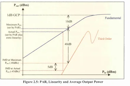
2.1.5 Peak to A verage R atio, B ack-O ff and Efficiency
Peak-to-A verage Ratio (PA R ) is a significant issue in multicarrier system s, as it has a great
impact on efficien cy. General literature indicates that W C D M A needs 10-13dB and
multicarrier EDG E/G SM (> 6 carriers) requires about 10-12dB o f Peak-to-Average
'headroom’. This refers to the m inim um amount o f b a ck -o ff required to prevent the am plifier
output saturating, regardless o f any other considerations. Figure 2.5 sh ow s this graphically
for the case o f an input signal with a PAR o f lOdB, assum ing a tw o-tone linearity
requirement o f -45dB c.
Pout (dBm )
IdB G C P
-Fundamental lOdB
Maximum Pave (set by PAR)__
Actual Pave ••• (set by PAR plus
extra linearity) Third-Order
40dB
IMD at Maximum Pave(40dBc)
-5dB
IMD at Actual
Pave (-45dBc)' Pin (dBm )
Figure 2.5: PA R , L inearity and A verage O utput P ow er
Referring to the above figure, the th e o retica l maximum average output pow er is less than the
IdB G ain-Com pression Point power by an amount equal to the signal PAR. In this exam ple,
the tw o-tone linearity at this level o f b a ck -o ff is only 40d B c, so the extra 5dB o f linearity