An Analysis and Design of Semi-Dual Active
Bridge Converter by Using MATLAB Simulink
Jigar Patel1, Hinal Surati2, Ashish Chaudhari3
PG Student [PS], Dept. of EE, CGPIT, Bardoli, Gujarat, India1 Assistant Professor, Dept. of EE, CGPIT, Bardoli, Gujarat, India2 Assistant Professor, Dept. of EE, CGPIT, Bardoli, Gujarat, India3
ABSTRACT: The use of DC-DC Converters has been increased for high power applications i.e., power flow is from source to load. As per this conversion switch stress, voltage regulation, reliability, high efficiency, cost etc., comes into picture. However the converter with more reliability, less weight, less cost is much preferred.For power conversion applications requiring bidirectional power flow, the dual active bridge (DAB) is a preferred topology. Semi-dual active bridge (S-DAB) converter is obtained from Dual Active bridge converter (DAB) by replacing two switches(MOSFET or IGBT) to the two diodeson the load side. As the no of switches are less when compared to dual Active Bridge converter (DAB), it has high efficiency, unidirectional power flow and less stress on switches.Along with the above advantages it undergoes Zero Voltage Switching (ZVS) is achieved such that switching loss is less. This topology is for unidirectional power flow and its applications for photovoltaic power converter, battery charger for electrical vehicles. MATLAB Simulink of semi-dual active bridge converter is designed.
KEYWORDS: Semi-dual active bridge (S-DAB), Dual Active Bridge (DAB), Zero voltage switching (ZVS), Sinusoidal pulse width modulation(SPWM).
I. INTRODUCTION
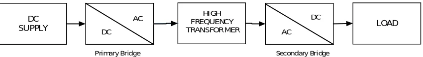
Since then the converter has gained popularity because of its high power density, high efficiency due to ZVS operation under wide load range, bidirectional operation and high frequency isolation. The traditional control of the converter is based on phase shift modulation.The benefits of the soft-switching are reduced switching losses, switch stress, low electromagnetic interference and easier thermal management. Hence this converter can be used for the high power density aerospace applications, photovoltaic power converter, battery charger etc. Converters are different types AC-AC, AC-DC, DC-DC, DC-AC etc. as per conversion. The block diagram of S-DAB is shown in fig. 1.
DC SUPPLY
AC
DC AC
DC HI GH
FREQUENCY TRANSFORMER
Primary Bridge Secondary Bridge
LOAD
Figure 1 Block diagram of Semi dual active bridge converter
There are different types of converter as follows:
Non-isolated converter
Isolated converter
This paper deals with semi-dual active bridge converter which is isolated converter.
II. CIRCUIT TOPOLOGY OF SEMI-DUAL ACTIVE BRIDGE CONVERTER
The semi-dual active bridge converter is proposed as a unidirectional DC-DC conversion as shown in fig. 2
S1 S3
S2 S4 S2s S4s
C1
C2
C3
C4
PRIMARY SIDE BRIGE
L
1:N HIGH FREQUENCY
TRANSFORMER +
-+
-Vs
D1s D3s
C1s C3s
C2s C4s
Co RL
SECONDARY SIDE BRIGE i
iL
io
Figure 2 proposed semi-dual active bridge converter topology
The S-DAB has two Bridges, the first one is consisting of four MOSFETs or IGBTs with antiparallel diodesand capacitors are connected across the switches. In the secondary side of transformer the upper switches are MOSFETs which are replaced by diodes. This two bridges are connected by High frequency transformer that gives a galvanic isolation and step-up and step-down the voltages. Inductor is connected at the primary side of the transformer i.e. leakage inductance. The both the Primary and secondary bridges having driven by square waveforms and 50% duty cycle.
III. OPERATION OF SEMIDUAL ACTIVE BRIDGE CONVERTER
The gate pulses of 50% duty cycles are shown in fig. 3. The converter output depends on the modulation index (m).
Where, m =
Figure 3Operation for mode-1 Figure 4 Operation for Mode-2
In mode-1 in primary bridge the 2nd and 3rd switch are off. So that current flows through the diodes of 1st and 4th switch and Dbs and Dcs. As the current across the inductor increases and capacitors are charge and discharge. Such that the switches are turn ON and turn OFF simultaneously. Thus the all modes are operated according to as switching takes place.
Figure 5 Operation for Mode-3 Figure 6 Operation for Mode-4
Figure 7 Operation for mode-5 Figure 8 Operation for Mode-6
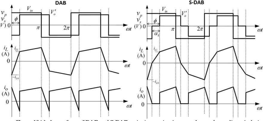
Figure 9 S-DAB Waveforms for m<1 and m>1. Primary and secondary voltage, inductor current.
Comparative waveforms of DAB and S-DAB. In which the fig. shows that the output current of DAB having negative pulses but in S-DAB because of diodes current in negative side is absent.
IV. SEMI-DUAL ACTIVE BRIDGE CONVERTER IMPLEMENTED IN MATLAB SIMULINK
The block diagram of S-DAB is shown in figure 10.
HB1 HF
Transformer HB2 LOAD
Driver Circuit Driver Circuit 230V AC Supply DC SUPPLY
Figure 11 Block diagram of S-DAB for MATLAB Simulink The MATLAB Simulink model of semi-dual active bridge converter is shown in fig.11
Figure 12 MATLAB Simulink model of Semi-dual Active bridge converter
V. OUTPUT WAVEFORMS
Waveforms of the simulated Semi-dual active bridge converter for m<1 i.e. buck operation is shown in figure 13,14,15,16. And for m>1 i.e. boost operation inductor current and secondary voltage (Vs) are shown.
Discrete, Ts = 5e-005 s.
powergui v +-V4 v + -V2 v + -V1 v + -V G1 G2 G3 G4 Subsystem Scope9 Scope6 Scope5 Scope4 Scope2 Scope10 Scope1 Scope g m C E S4 g m C E S3 g m C E S2 g m C E S1s g m C E S1 g m C E S L1 L i + -I3 i + -I2 i + -I1 i +
-I 1 2
Figure 13 Primary voltage (Vp)
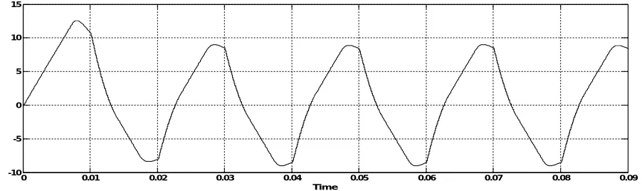
Figure 14 Inductor current (IL)
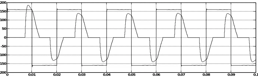
Figure 15 transformer’s primary and secondary side voltages. That shows the buck operation (m<1)
0 0.05 0.1 0.15 0.2 0.25 0.3 0.35 0.4 0.45 0.5
-150 -100 -50 0 50 100 150
Time(Sec)
V
o
lt
a
g
e
(
V
)
0 0.01 0.02 0.03 0.04 0.05 0.06 0.07
-6 -4 -2 0 2 4 6 8
Tim e
0 0.01 0.02 0.03 0.04 0.05 0.06 0.07 0.08 0.09 0.1
-200 -150 -100 -50 0 50 100 150 200
Time
Now for boost operation (m>1)
Figure 17 Inductor current (iL)
Figure 18 Primary voltage and secondary voltage that shows boost operation.
The input gives to primary bridge 160V and it gives the pulsating DC voltage of 160V. And then step down this voltage by transformer.
VI. CONCLUSION
The Semi-dual active bridge converter has been implemented in MATLAB and switches has been used MOSFET and this switches has been drive using SPWM (Sinusoidal Pulse Width Modulation). As comparing with DAB the soft switching has been achieved by using capacitors connected across the switches and diodes. Hence output Voltage of S-DAB has been higher than the S-DAB output voltage. So that the losses in the S-DAB reduced by the other topology named S-DAB and then the losses decreases, the efficiency of the S-DAB converter is high and switches are less as compared so that the cost is also less.
REFERENCES
[1] GundaKavya, Muni DivyaSreeVachana, A. Sumathi, Subramanian. K “Matlab/Simulink Based Closed Loop Operation of Semi dual active
bridge Converter”. IEEE 2014.
[2] SiddharthKulasekaran and RajpandianAyyanar, “Analysis, Design and Experimental Results of the Semi-dual active bridge Converter”. IEEE
Tran. On Power Electronics, Vol. 29, No. 10, October 2014.
[3] Narsimharaju B. L., VenkataPrahalad, Ramanjennya Reddy, Vijay babu, Srinivasan, “Optimization of Bidirectional Dual Active Bridge DC–
DC Converter for UPS Application”. IEEE International Conference on Power Electronics, Drives and Energy System, 2014.
[4] R. T. NAAYAGI, N. E. MASTORAKIS, “Performance Verification of Dual Active Bridge DC-DC Converter”, Recent Researches in
Applications of Electrical and Computer Engineering, ISBN: 978-1-61804-074-9.
[5] Robert L. SteigerwaldRik W. De DonckerMustansir H. Kheraluwala, A Comparison of High Power DC-to-DC Soft-Switched Converter
Topologies, 0-7803-1993-1/94 1994 IEEE.
0 0.01 0.02 0.03 0.04 0.05 0.06 0.07 0.08 0.09
-10 -5 0 5 10 15
Tim e
0 0.05 0.1 0.15 0.2 0.25
-400 -300 -200 -100 0 100 200 300 400 500
Time
V
o
lt
a
g
e
(V