Dopant compensation in alloyed
CH
3
NH
3
PbBr
3
−
x
Cl
x
perovskite single crystals for
gamma-ray spectroscopy
Haotong Wei
1†, Dylan DeSantis
2†, Wei Wei
1, Yehao Deng
1, Dengyang Guo
3, Tom J. Savenije
3, Lei Cao
2and Jinsong Huang
1,4*
Organic–inorganic halide perovskites (OIHPs) bring an unprecedented opportunity for radiation detection with their defect-tolerance nature, large mobility–lifetime product, and simple crystal growth from solution. Here we report a dopant compensation in alloyed OIHP single crystals to overcome limitations of device noise and charge collection, enabling
γ-ray spectrum collection at room temperature. CH3NH3PbBr3 and CH3NH3PbCl3 are found to be p-type and n-type
doped, respectively, whereas dopant-compensated CH3NH3PbBr2.94Cl0.06alloy has over tenfold improved bulk resistivity of
3.6
×
109cm. Alloying also increases the hole mobility to 560 cm2V−1s−1, yielding a high mobility–lifetime product of1.8
×
10−2cm2V−1. The use of a guard ring electrode in the detector reduces the crystal surface leakage current and devicedark current. A distinguishable137Cs energy spectrum with comparable or better resolution than standard scintillator detectors
is collected under a small electric field of 1.8 V mm−1at room temperature.
T
he strong penetrating capability of high-energy ionizing photons (for example, X-ray or γ-ray) enables the non-invasive detection of condensed objects with radiation detectors that are widely used in many fields including medical imaging, shipping container inspection, radiological and nuclear defence, environmental monitoring, decontamination, homeland security, academic research and so on1–3. In addition to radiation dose, the energy spectrum of ionizing photons is another important piece of information that must be known for many applications, such as radioactive species identification. Unlike intensity-mapping-based X-ray radiography, γ-ray energy spectrum detection needs a detector to work in pulse mode, under which the radiation field is typically much weaker than that in current mode, and the detector is performing event-by-event analysis to sort out the intensity versus energy of the radiation quanta. The energy-resolved spectrum is constructed by histogramming the electrical pulse height produced by photons interacting with the detector’s material. Therefore, the objective of obtaining a good-resolution energy spectrum imposes strict requirements to radiation detection materials, as well as the sizes of materials in terms of competition with Schubweg distance. Semiconductor radiation detectors for high-energy-photon detection require materials with a large detecting volume to intercept radiation, a large linear attenuation coefficient, large and balanced electron and hole mobility (µ)–charge carrier lifetime (τ) product (µτproduct) for efficient charge collection, and finally, high resistivity and low charge trap density to avoid charge trapping under single-event analysis4. Among the semiconductors with relatively strong attenuation, high-purity germanium (HPGe) that was developed in the 1970s gives a γ-ray detector the best resolution, which however needs liquid nitrogen cooling due to its small bandgap5.Zinc-alloyed CdTe (Cd1−xZnxTe, denoted CZT for 0<x<0.2) single crystals with a large bandgap of above 1.6 eV possess a high resistivity up to 108
∼
109cm at room temperature as well as a large µτ product, and thus produce the best resolution γ-ray spectrum among non-cooled semiconductor radiation detectors6–8. However, there are many limitations for the application of CZT detectors, such as the cost-restricted crystal manufacturing at a scaled up level, the incompatibility of high-temperature crystal growth with read-out circuits, and low hole mobilities7,8. The slow development progress of the CZTγ-ray detector is heavily limited by the material development.Organic–inorganic halide perovskites (OIHPs), which have made significant successes in the applications of solar cells9,10, light-emitting diodes11 and photodetectors12, are showing a great promise as a new generation of radiation detection materials13–17. In addition to their largeµτproduct, these materials in a single-crystal form have a low charge trap density and defect-tolerant nature, making them particularly attractive for radiation detection15,16,18. High-quality perovskite single crystals can be grown from a solution at room temperature with low-cost raw materials15,16,19. The high atomic number (Z) of Pb, I and Br as well as the relatively large material density of about 4.0 g cm−3enables respectable attenuation of high-energy photons13,14,16. We reported the largeµτproduct of methylammonium lead triiodide (MAPbI3) single crystal and its application in gamma-ray energy harvesting with a 4% efficiency operated in a gammavoltaic mode15. Later the CH
3NH3PbBr3 single-crystal X-ray detectors were shown to have a high sensitivity of 80µC Gy−1
air cm
−2 to 50 keV X-rays with the lowest detectable dose rate of 0.5µGyairs
−1, which is already several times more sensitive than the commercial amorphous selenium (α-Se) X-ray detectors16. Recently, the integration of perovskite single crystals
1Department of Mechanical and Materials Engineering, University of Nebraska-Lincoln, Lincoln, Nebraska 68588, USA.2Nuclear Engineering Program,
Department of Mechanical and Aerospace Engineering, Ohio State University, Columbus, Ohio 43210, USA.3Optoelectronic Materials Section,
Department of Chemical Engineering, Delft University of Technology, 2628 BL Delft, the Netherlands.4Department of Applied Physical Sciences,
Free holes Free electrons
Dopant-compensated CH3NH3PbBr2.94Cl0.06 CH3NH3PbCl3
107
108
CH3NH3PbBr2.94Cl0.06
Majority carrier concentration (a.u.)
p type
CH3NH3PbBr3
1 2 3 4 5
108
107
CH3NH3PbCl3 CH3NH3PbBr2.4Cl0.6 CH3NH3PbBr2.85Cl0.15
Magnet rotation cycle n type
CH3NH3PbBr3
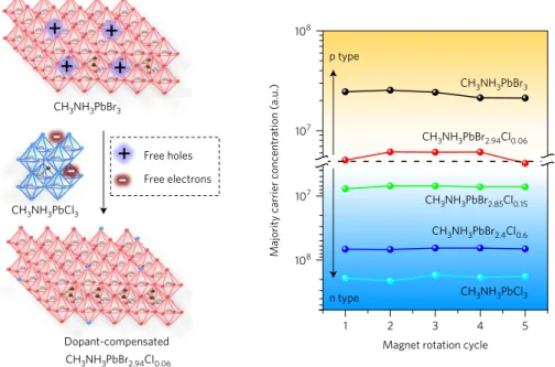
Figure 1| Cl−alloying for dopant compensation.a, Scheme of dopant compensation of CH3NH3PbBr2.94Cl0.06single crystal.b, Hall effect results to reveal
the majority carrier type of CH3NH3PbBr3−xClxsingle crystals.
with silicon substrates has been demonstrated, which not only further enhanced the sensitivity to 2.1
×
104µC Gy−1air cm
−2 under lower limit of the carrier concentration, the dark conductivity ofsingle crystals inγ-ray detectors can be many orders of magnitude larger, often originating from unintentional doping effects by defects or impurities. High-purity raw materials or more sophisticated crystal growth processes are generally employed to improve the crystal quality, yet this increases the cost dramatically and limits the throughput of material production. For many materials, including OIHPs, the unintentional doping cannot be completely eliminated by improved crystal growth due to the thermodynamic stability of certain defects, which, in high concentrations, can dominate the device’s dark current. Density functional theory calculations predict that Pb2+
vacancies and Br−vacancies are dominant shallow acceptors and shallow donors in CH3NH3PbBr3, respectively. Since the formation energy is lower for Pb2+
vacancies than for Br− vacancies in most synthesis conditions, CH3NH3PbBr3 is expected to exhibit a weak unipolar p-doping20. It should be noted that the defect formation energy is also dependent on the position of the Fermi level. Experimentally, CH3NH3PbBr3 single crystals, synthesized by several methods, demonstrate a p-type conduction by Hall-effect measurements with a resistivity of about 2.0
×
108cm (ref. 19), which is over tenfold smaller than that of the state-of-the-art CZT single crystals.Interestingly, we noticed that the as-synthesized CH3NH3PbCl3 single crystals are n-type from Hall effect measurements, and thus had a hypothesis that Cl− ion vacancies may form more easily than Br−ion vacancies. Since Cl−ion vacancies are also expected to be shallow donors, it is reasonable to speculate that Cl−
al-loying can reduce the hole density and increase the resistivity of the perovskite crystals. This dopant compensation scheme is il-lustrated in Fig. 1a. To test it, CH3NH3PbBr3−xClx single crys-tals with different Cl−
percentages were grown from solution by the inverse temperature crystallization method21, where the Cl−/(Br−
+
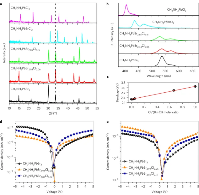
Cl−)molar ratio was tuned by changing the feeding ra-tio of CH3NH3PbBr3/CH3NH3PbCl3. The powder X-ray diffraction (XRD) spectra in Fig. 2a show that all of the diffraction peaks gradu-ally shift to larger angles as the Cl−molar ratio in the precursor solu-tion is increased from 1.37% to 52.7%, indicating a successful incor-poration of Cl−into the lattice. The actual Cl−/(Br−
+
Cl−)molar ratio in the crystals is calculated on the basis of the shift of the (012) diffraction peak by assuming the effectiveness of Vegard’s law21. 8keVX-rayradiation,butalsoallowedadirectsignalread-outwithsilicon-based circuits17. The demonstrated imaging capability at extremelylowdoseratesmayfinditsapplicationinmedicalimaging devicestominimizetheX-raydosagetowhichpatientsareexposed. DespitethesignificantprogressmadeonX-raydetectorsoperating incurrentmode,thecapabilityofproducinggood-resolutionenergy spectra by perovskite detectorsworking in pulse-height analysis moderemainsamajorchallenge.Recently,aformamidiniumlead triiodide (FAPbI3) single-crystal detector, which is intrinsically notstableat roomtemperature,wasreportedtohaveacquireda 59.6keV 241Amenergyspectrum13.However,ahigh-energyγ-ray spectrumremainsunobtainableasalargersizedetectorisrequired, bywhichahighµτEproduct(Eistheappliedelectricfield)and alargebulkresistivityaredesired.Alargeelectricfieldcouldbe appliedtoenhancethedriftlengthofchargecarriersandreduce theirtrappingbydeepchargetraps,buttheincreasedelectricfield alsoincreasesdarkcurrentornoise.Therefore,theµτ productof thematerialsshouldbelargeforastrongsignal.However,alarge mobilityalsoincreasesdarkcurrent,whichisproportionaltocarrier mobility;thus,thedirectiontoreducedarkcurrentnoiseistoreduce thematerial’sintrinsicchargecarrierconcentration.
In this article, we report the acquisition of the 137Cs energy spectrumwithalow-costperovskitesingle-crystalγ-raydetectorby suppressingthedevice’snoisewhileretainingastrongsignalwith dopantcompensationofCH3NH3PbBr3.Thedopantcompensation byCl−alloyingofp-typeCH3NH3PbBr3singlecrystaldramatically reducesthechargecarrierconcentrationinthebulkcrystal,while thecarriermobilityandlifetimehavebeenimprovedsignificantly, enhancing the charge collection efficiency. In addition, a guard ringelectrodewasimplementedtoreducethesurface/edgeleakage currentthatcouldotherwisecorruptthesignal.Theimproved sig-nal/noiseratioresultedinawell-defined137Csenergyspectrumby operatingthedeviceunderalowelectricfieldatroomtemperature.
Dopantcompensationtoreducedarkcurrent
0.0 0.2 0.4 0.6 0.8 1.0 2.1
2.4 2.7 3.0 3.3
Bandgap (eV)
Cl/(Br+Cl) molar ratio
400 450 500 550 600 650
CH3NH3PbBr3
Wavelength (nm) CH3NH3PbBr2.94Cl0.06
PL intensity (a.u.)
CH3NH3PbBr2.85Cl0.15
CH3NH3PbBrCl2
CH3NH3PbCl3
10 15 20 25 30 35 40 45 50 55
Intensity (a.u.)
2θ (°)
CH3NH3PbBr3
CH3NH3PbBr2.94Cl0.06 CH3NH3PbBr2.85Cl0.15
CH3NH3PbBrCl2
CH3NH3PbCl3
a b
c
d
10−5
10−4
10−3
CH3NH3PbBr3
CH3NH3PbBr2.94Cl0.06 CH3NH3PbBr2.85Cl0.15
−5 −4 −3 −2 −1 0 1 2 3 4 5
10−7
10−6
10−5
10−4
CH3NH3PbBr3
CH3NH3PbBr2.94Cl0.06 CH3NH3PbBr2.85Cl0.15
Current density (mA cm
−2)
Current density (mA cm
−2)
Voltage (V)
−5 −4 −3 −2 −1 0 1 2 3 4 5
Voltage (V) e
Figure 2| Cl−alloying to suppress dark current.a, XRD spectra of CH3NH3PbBr3−xClxsingle-crystal powder with different Cl−ratios.b, Corresponding
photoluminescence (PL) spectra of CH3NH3PbBr3−xClxsingle crystals.c, Bandgap shift versus Cl/(Br+Cl) ratio.d, Dark current density of CH3NH3PbBr3,
CH3NH3PbBr2.94Cl0.06and CH3NH3PbBr2.85Cl0.15single-crystal devices with thickness of∼2 mm.e, Photocurrent of CH3NH3PbBr3,
CH3NH3PbBr2.94Cl0.06and CH3NH3PbBr2.85Cl0.15single-crystal devices under ambient light with thickness of∼2 mm.
The crystals grown with Cl−
feeding ratios of 1.37% and 4.90% have Cl−/(Br−
+
Cl−)molar ratio of 2.0% and 5.1%, giving compositions of CH3NH3PbBr2.94Cl0.06and CH3NH3PbBr2.85Cl0.15, respectively. In addition, a continuous blueshift of the photoluminescence emis-sion peak was also observed with the increase of the Cl−ratio, as shown in Fig. 2b. The bandgap derived from the main photolu-minescence emission peak presented a linear relationship with the actual Cl−
/(Br−
+
Cl−) molar ratio in the crystals, as shown in Fig. 2c. It is noted that, in photoluminescence emission spectrum, the shoulder peak at longer wavelength range can be assigned to the optical reflection of the photoluminescence from the back surface of the single crystal22. After confirming the successful Cl−
alloying, we measured the majority carrier types of the CH3NH3PbBr3−xClx single crystals by Hall effect, and verified that addition of Cl−
into the p-type CH3NH3PbBr3 converted the crystals to n-type when 20% of Cl−was added, while CH3NH3PbBr2.94Cl0.06is very close to being intrinsic, as shown in Fig. 1b.
We then directly compared the conductivity of a
CH3NH3PbBr2.94Cl0.06single crystal with a control CH3NH3PbBr3 single crystal that has a similar thickness of about 2 mm. A device structure of Cr/CH3NH3PbBr3−xClx/C60/bathocuproine (BCP)/Cr
was used. Figure 2d shows that the dark current density of the CH3NH3PbBr2.94Cl0.06device under
−
5 V is more than five times smaller than that of the control CH3NH3PbBr3device, indicating that the p-type-doped CH3NH3PbBr3 is effectively compensated by Cl−repro-0 5 10 15 20 90 100 0
100 200 300 400 500 600
Hole mobility Electron mobility
ToF mobility (cm
2 V −1 s −1)
Hole mobility (cm
2 V −1 s −1)
Cl/(Cl+Br) (mol%)
106
107
108
109
1010
Charge carrier concentration (
cm
−3
)
a
200 240 280
µ ∝ T−3/2
320
102
103
CH3NH3PbBr3
CH3NH3PbBr2.94Cl0.06
CH3NH3PbBr2.85Cl0.15
Temperature (K)
0 20 40 60
101
102
CH3NH3PbBr3
CH3NH3PbBr2.94Cl0.06
CH3NH3PbBr2.85Cl0.15
Photocurrent (nA)
Voltage (V)
0 1 2 3 4 5
10−2
10−1
100
Δ
P
/
PI0
(a.u.)
Time (μs)
CH3NH3PbBr3
CH3NH3PbBr2.94Cl0.06
CH3NH3PbBr2.85Cl0.15
b
c d
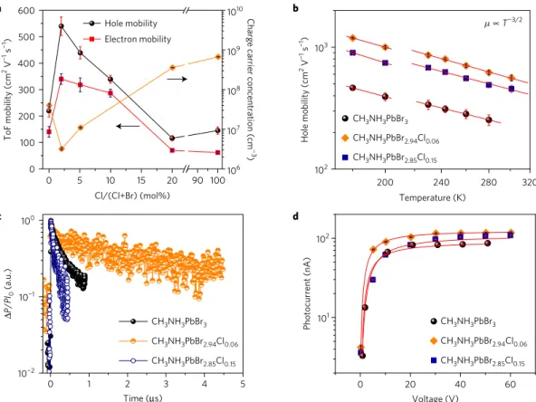
Figure 3| Mobility andµτproduct improvement.a, Hole and electron mobilities of the CH3NH3PbBr3−xClxsingle crystals by ToF technique. Error bars are
given according to the variation of single-crystal thicknesses.b, Hole mobility of CH3NH3PbBr3−xClxsingle crystals versus temperature.c, Time-resolved
microwave conductance traces of the CH3NH3PbBr3−xClxsingle crystals.d, Photoconductivity of the CH3NH3PbBr2.94Cl0.06single crystal with a thickness
of∼2 mm.
mobility, they are still within the same order of magnitude. The ToF electron mobility is also in accordance with the mobility measured by the space-charge-limited current (Supplementary Fig. 4).
High-quality perovskite single crystals provide a platform to study the intrinsic mobility of perovskite due to the absence of grain boundary16,19,23,24. The carrier mobility is determined by the carrier’s effective mass (m∗
) and the average scattering (or momentum relaxation) time (τ0) via the relationship µ
=
eτ0/m∗, wheree is the elementary charge25,26. The calculated effective mass of CH3NH3PbBr3is comparable to that of silicon27, giving the materials a potential to exhibit a large mobility of over 1,000 cm2V−1s−1at room temperature, which is greater than the previously measured values28,29. The enhanced carrier mobility indicates that the carrier scattering caused by dopants or charged centres may be limiting the carrier mobility in perovskite. Calculation results predicted that Cl−
alloying in I−
-based perovskite would extend the carrier’s thermalization time30, which was mainly caused by the structural deformation of PbI4−
6 octahedra and lattice parameter changes after Cl−alloying. To identify the relationship between temperature and carrier scattering, the temperature-dependent ToF hole mobility of CH3NH3PbBr3−xClxsingle crystals was measured from 300 K to 180 K, with the results displayed in Fig. 3b (ToF curves are shown in Supplementary Figs 5–7). With the exception of a discontinuity at 225 K, the mobilities presented a clearT−1.5dependence for all three single-crystal devices at temperatures both above and below the cubic phase to tetragonal phase transition temperature (225 K) (ref. 31). Therefore, the high hole mobility of 560
±
46 cm2V−1s−1 at 300 K and∼
1,200±
50 cm2V−1s−1at 180 K provides evidence of the increased electronic quality of the CH3NH3PbBr2.94Cl0.06 single crystals.The reduction of the charged dopant centre may also impact the charge carrier recombination process. As presented in Fig. 3c, the ducibilityofelectronicpropertiesofthesecrystals.Thedarkcurrent
andphotocurrentof thedevicesalmost overlapwitheach other, confirmingthegoodreproducibility(seeSupplementaryFig.1).
Increasedcarriermobilityandlifetime
We further studied the charge carrier mobility in the single crystalsto understandtheimproved chargecollectionefficiency. The electron and hole mobilities of CH3NH3PbBr3−xClx single crystals were measured by the time-of-flight (ToF) technique. Here, C60 andBCPwere subsequently depositedonthecathode sideasanelectron-accepting/transporting layer,therebyenabling a fast extraction of photon-generated electrons as well as the reductionofchargeinjectionunderreversebias.Figure3ashows that the ToF hole mobility of the CH3NH3PbBr3 single crystal isabout220
±
20cm2V−1s−1 atroom temperature,whichagrees with previously reported results16. The addition of 2.0% Cl− into CH3NH3PbBr3 dramatically increased the hole mobility to 560±
46cm2V−1s−1. Further increasing the Cl−percentage to 20% reduced the hole mobility to 130
±
15cm2V−1s−1, which is comparable to that of the CH3NH3PbCl3 single crystal. The ToF curves of the single-crystal devices with 0%, 2.0% and 5.1% Cl− alloying are shown in Supplementary Fig. 2, and the corresponding electronic property statistic distribution of four devicesforeachcompositionisdescribedinSupplementaryFig.3. Electronmobilityfollowedthesametrendastheholemobility.The ToFelectron mobilityofCH3NH3PbBr3 singlecrystal isroughly 140±
17cm2V−1s−1, and increases to 340±
20cm2V−1s−1 for crystalswith2.0% Cl− alloying, andthen graduallydecreases to 320±
30cm2V−1s−1for5.1%Cl−0.3 0.4 0.5 0.6 106
107
108
109
10
DOS (cm
−3 eV −1)
E(ω) (eV) CH3NH3PbBr3 CH3NH3PbBr2.94Cl0.06 CH3NH3PbBr2.85Cl0.15
a b
1 2 3 4 5 6 7 8
10−1
100
101
10
22 nW cm−2
2.5 nW cm−2
230 pW cm−2
8 pW cm−2
Dark Shot noise
Signal current (pA Hz
−1/2
)
Frequency (Hz) 100
101
102
CH3NH3PbBr3 CH3NH3PbBr2.94Cl0.06 CH3NH3PbBr2.85Cl0.15
IQE (%)
400 450 500 550 60010
9
1010
1011
1012
Specific detectivity
Specific detectivity (Jones)
Wavelength (nm)
101 102 103 104
−3 −2 −1 0
CH3NH3PbBr3 CH3NH3PbBr2.94Cl0.06 CH3NH3PbBr2.85Cl0.15
Relative response (dB)
Light modulation frequency (Hz)
c
d f
0 20 40 60 80 100
−40 −30 −20 −10 0
Dark current (nA)
Time (min)
0 10 20 30 40 50 60 70
3.0 3.5 4.0 4.5 5.0 5.5
CH3NH3PbBr3 CH3NH3PbBr2.94Cl0.06 CH3NH3PbBr2.85Cl0.15
Current density (
µ
A cm
−2)
Time (s) e
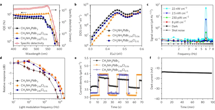
Figure 4| Photodetector performance.a, IQE of the CH3NH3PbBr3−xClxsingle-crystal devices and specific detectivity of the CH3NH3PbBr2.94Cl0.06
single-crystal device under−5 V with a thickness of∼2.4 mm.b, Trap density of states of the CH3NH3PbBr3−xClxsingle-crystal devices with different
Cl−ratios.c, Noise current and directly measured NEP of the CH3NH3PbBr2.94Cl0.06single-crystal device with a thickness of∼2.4 mm under−5 V.
d, Temporal response of the CH3NH3PbBr3−xClxsingle-crystal device with a thickness of∼2.4 mm under−5 V. Error bars are given according to the
variation of photocurrent signal.e, Dark current and photocurrent stability of the CH3NH3PbBr3−xClxsingle-crystal device under electrical field of
0.11 Vµm−1.f, Long-term dark current stability of the CH3NH3PbBr2.94Cl0.06single-crystal device under electrical field of 1.8 V mm−1.
carrier recombination lifetime in the single crystals was studied by time-resolved microwave conductance, where a 570 nm laser pulse was utilized to generate free charges. Since photons with 570 nm wavelength can fully penetrate the bulk of the single crystal, charges are generated not only at the surface but also inside the single crystal. A weak nanosecond laser pulse of 5.4
×
1013photons per square centimetre per pulse was successfully used for excitation. A lifetime of∼
5µs was recorded for the CH3NH3PbBr2.94Cl0.06 single crystals, which is a tenfold increase as compared with that of CH3NH3PbBr3 and CH3NH3PbBr2.85Cl0.15 single crystals. Since the charge recombination lifetime is strongly dependent on the photo-generated carrier concentration, we continued to evaluate the µτ product at even weaker light intensities to emulate the working condition of the devices under naturally occurring gamma radiation. As seen in Fig. 3d, the steady-state photoconductivity curve of the CH3NH3PbBr2.94Cl0.06single crystal, induced by a 1.2×
1012photons cm−2s−1 light source, reveals aµτ product of(1.8±
0.2)×
10−2cm2V−1as well as an extremely low surface recombination velocity of 55 cm s−1. Theµτ product is larger than that of CH3NH3PbBr2.85Cl0.15single crystals ((1.5±
0.2)×
10−2cm2V−1) and CH3NH3PbBr3 single crystals ((1.1
±
0.2)×
10−2cm2V−1).Photon detection performance
With increased carrier mobility and recombination lifetime, we hypothesize that the charge collection would be improved in CH3NH3PbBr2.94Cl0.06detectors compared with the CH3NH3PbBr3 or CH3NH3PbBr2.85Cl0.15 detectors. Therefore, to characterize the charge collection efficiency (CCE) or the internal quantum efficiency (IQE), the external quantum efficiency (EQE) of the CH3NH3PbBr2.94Cl0.06 single-crystal device was measured under a reverse bias. The CCE was then equated as the ratio of the EQE to the electrode transparency. As shown in Fig. 4a, the CCE of the 2.4-mm-thick CH3NH3PbBr2.94Cl0.06 single-crystal
device reached 100% under a
−
5 V, slightly better than that of the CH3NH3PbBr2.85Cl0.15 device, but twofold larger than that of the CH3NH3PbBr3 device, which can be attributed to the largerµτ product and thus longer drift length of CH3NH3PbBr2.94Cl0.06 single crystal. The frequency response of the CH3NH3PbBr2.94Cl0.06 single crystal under
−
5 V can be seen in Fig. 4d, in which the bandwidth is evaluated as 15.2 kHz. This in turn corresponds to a response time of 23µs, which is close to the calculated transit time of 21µs by a hole mobility of 560 cm2V−1s−1. Here the transit time is calculated byt=
d2/µV, wheredis the thickness and V is the applied voltage. In addition to high mobility, the CH3NH3PbBr2.94Cl0.06single crystals should also have a low charge trap density; otherwise a fast response time would be unlikely given the long charge trapping and detrapping time from the deep traps. The thermal admittance spectroscopy measurement provides the trap density of states in the single-crystal devices, as shown in Fig. 4b. The dopant-compensated CH3NH3PbBr2.94Cl0.06device has nearly a tenfold reduction of charge traps when compared with the CH3NH3PbBr3 single-crystal device. Such a reduction can be attributed to the compensation of the p-type dopants. It is noted that while the trap density remains unchanged for the CH3NH3PbBr2.85Cl0.15 single-crystal device when considering the deep trap depth, it is slightly higher in the shallow trap depth range, which may be caused by the additional Cl−n-type dopant.Just as both low trap density and device dark current are crucial factors on the performance of weak-light-sensitive photodetectors, so too are they important factors on the performance of high-energy
8 pW cm−2, which in turn converts to a NEP of 1.3 pW Hz−1/2, comparable to the calculated NEP of 2 pW Hz−1/2 from device responsivity and directly measured noise. A high specific detectivity
D∗
of 2.5
×
1012jones was derived from the IQE and measured noise current. It is noted that IQE is used here for evaluation, because high-energy photons can easily penetrate the thin metal electrode. Finally, the device’s response to X-rays with varying dose rates was also measured. The device sensitivity to 8 keV X-rays was derived from the slope of the straight line of the output current density versus the X-ray dose, which reaches 8.4×
104µC Gy−1aircm
−2with
change after dopant compensation into consideration, as shown in Fig. 3a (details of the calculation are presented in Supplementary Table 1), in agreement with the Hall effect result presented in Fig. 1b. The energy resolution is the most important figure of merit to evaluate how well a detector can resolve the fine energy lines from nuclear decay. A detector for pulse-height analysis should firstly have a large size, or footprint, to stop high-energy γ-ray radiation and secondly, a large µτE product, that is, the mean free path of free charge carrier, to outperform the physical length of the detector. We confirmed the µτE product of our crystals under 1.8 V mm−1 is larger than the crystal thickness. Utilizing enhancements by guard rings, the 137Cs energy spectrum was obtained with three CH3NH3PbBr2.94Cl0.06 single-crystal devices (named as device I, II and III). The crystals I, II and III have dimensions of 1.30
×
1.25×
0.37 cm3, 1.44×
1.37×
0.58 cm3, and 1.06×
1.00×
0.49 cm3, respectively, and a photo of single crystal II is shown in the inset of Fig. 5e. A 5.0µCi137Cs source was placed 10 cm from the anode of the CH3NH3PbBr2.94Cl0.06detector, which was connected to a charge-sensitive preamplifier (Ortec-142A) and processed with a DSP (Ortec DSPEC 50). A typical137Cs energy spectrum was acquired by the CH3NH3PbBr2.94Cl0.06 (device I) detector under an electric field of 1.8 V mm−1at room temperature as shown in Fig. 5f, and two other spectra collected by two other CH3NH3PbBr2.94Cl0.06 detectors are shown in Fig. 5g (device II) and Fig 5h and Supplementary Fig. 9b (device III). Although each perovskite device has shown a different energy resolution and photopeak to Compton ratio40, which might be related to variation of contact qualities, the spectrum features, such as the Compton edge with respect to its energy, are consistently aligned with the the-oretical value and the energy scale calibrated by reference detectors. As a comparison, no photopeak or Compton edge was observed in the137Cs energy spectrum acquired by any CH3NH3PbBr3device, as shown in Fig. 5g, indicating the important role of high mobility and low free carrier concentration of CH3NH3PbBr2.94Cl0.06for spectrum collection. A CZT semiconductor detector (1.0 cm3 volume) and a NaI(Tl) scintillator (a cylinder of 7.62 cm diameter and 7.62 cm tall)-based detector were used for reference. As can be seen in Fig. 5f, the photopeak to Compton ratio is lower for CH3NH3PbBr2.94Cl0.06 than that of the CZT and NaI(Tl) reference detectors. This is mainly due to its small size, allowing a large fraction of Compton scattered photons to escape. It also partially owes to the small electric field that results in a long average electron transit time of 13µs as compared with the charge carrier recombination lifetime of about 32µs. Nevertheless, CH3NH3PbBr2.94Cl0.06 perovskite single crystal demonstrates desirable material properties for a good-resolution gamma spectroscopy, for instance, a large ratio of photoelectric to total cross-section,σpe/σtot, 0.24 at 662 keV as compared with CZT’s ratio of 0.08 (ref. 41). This, in theory, presents perovskite the potential to obtain a more prominent photopeak than an industry-leading room-temperature gamma-ray detector. The typical resolution of CH3NH3PbBr2.94Cl0.06detectors is around 12%, while the best CH3NH3PbBr2.94Cl0.06 device has a resolution of 6.50% (Fig. 5g). In comparison, the resolutions of the full-energy peaks are 2.27%, and 7.51% for CZT and NaI(Tl), respectively (Fig. 5f). It is shown that perovskite is capable of obtaining a resolution better than that obtained through a typical NaI(Tl) scintillator detector while being much more economical than standard semiconductor detectors used in industry. We estimated the raw material cost of CH3NH3PbBr2.94Cl0.06single crystals to be less than US$0.3 cm−3(see Supplementary Information). Moreover, the ability to grow high-quality perovskite crystals larger than 1.0 cm3 provides the potential for increased efficiency/cost ratio, which limits other semiconductor detectors such as CZT.
Finally, we studied the stability of the CH3NH3PbBr2.94Cl0.06 single-crystal detector using device III by measuring the variation of device charge collection efficiency and dark current over time. the lowest detectable dose rate of 7.6nGyair s−1, which is about
4,000-foldbetter thanthat ofcommercialα-SeX-raydetectors33 (SupplementaryFig.8a,b).
γ-rayenergyspectrumdetection
One major concern for the application of OIHP materials for radiationdetectionisthepolarizationeffectduetoionmigration, whichwouldresultinashiftoftheenergyspectrumaswellasa degradationofresolution34.Furthermore,ionmigration inOIHP polycrystalline films has been known to result in a switchable photovoltaiceffect35 aswellasbeanoriginofthecurrenthysteresis phenomenon in OIHP devices36. Despite the ion migration throughgraininteriors,wehaverevealedthatgrainboundariesin polycrystallinefilmsarefasterionmigrationchannels37.Therefore, the absence of grain boundaries in high-quality single crystals should suppress the polarization effect. Nevertheless, we still observedasmalldriftofboththedarkcurrentandphotocurrent for the control CH3NH3PbBr3 single-crystal device under an appliedelectricfieldof0.11Vµm−1 (Fig.4e),whichmaybecaused by ionmigration alongthecrystalsurfaceorpossibly bycharge trapping/detrapping effects. The CH3NH3PbBr2.94Cl0.06 single-crystaldevicedemonstratedanenhancedstabilityforboththedark currentandphotocurrentunderthesameelectricfield.Inpractice, theexcellentchargecollectionefficiencyandresponsespeedenable ourdetectortoworkunderalowelectricfieldof1.8Vmm−1,which retainsastabilizedsmalldarkcurrent.Wecontinuouslymonitored thedarkcurrentundertheelectricfieldof1.8Vmm−1 forabout 100min,andfoundthatthedarkcurrentdriftedonly
∼
1nAcm−2, or8%ofthedarkcurrent(Fig.4f).Theincreasedstabilitymaybe attributedto theincreasedattraction forcesbetweenthecation– anionpairoftheCl−anionsascomparedwiththeBr−
anions.The increasedattractionwouldineffectsuppressionmigrationthrough thecrystalsurface,agreeingwiththereducedtrapdensitymeasured.
Despite the reduction of polarization effects, the
a W/o guard electrical field
Working electrical field
Guard electrode (Cr)
Central electrode (Cr)
Cr
C60/BCP
With guard electrical field
Cr
C60/BCP
Cr
Guard electrical field
g
−750 −600 −450 −300 −150 0
−0.8 −0.6 −0.4 −0.2
0.0 Without guard ringWith guard ring
Current density (
μ
A cm
−2)
Electrical field (V cm−1)
R = 3.6 × 10⁹Ω cm
R = 9.7 × 10⁸Ω cm
f e
h
0 200 400 600 800 1,000
0 1 2 3 4 5 6
As synthesized After 35 krad
60Co irradiation
Relative count rate (a.u.)
Energy (keV)
0 200 400 600 800
0.0 0.2 0.4 0.6
CH3NH3PbBr3
CH3NH3PbBr2.94Cl0.06
Relative count rate (a.u.)
Energy (keV)
FWHM
b c d
0 200 400 600 800
0 2 4 6 8
Relative count rate (a.u.)
Energy (keV)
CH3NH3PbBr2.94Cl0.06
CZT NaI(Tl)
Figure 5|γ-ray detector performance.a, Electric field distribution of a single-crystal device with a guard electrode.b, Top view of the guard ring electrode
side of the detector.c, Top view of the anode side of the detector.d, Side view of a CH3NH3PbBr2.94Cl0.06single-crystal detector, and electrode sides were
encapsulated with epoxy.e, Dark current density of a CH3NH3PbBr2.94Cl0.06single-crystal device with and without a guard ring. The thickness of this
device is∼5.8 mm. Inset is a photograph of a centimetre-sized CH3NH3PbBr2.94Cl0.06single crystal for137Cs energy spectrum with dimension of
1.44×1.37×0.58cm3.f,137Cs energy spectrum obtained by CH3NH3PbBr2.94Cl0.06(device I), CZT and NaI(Tl) detectors.g, Enlarged photopeak region
of the137Cs energy spectrum obtained by CH
3NH3PbBr2.94Cl0.06(device II) and CH3NH3PbBr3single-crystal detectors. FWHM, full width at half
maximum.h,137Cs energy spectrum obtained by CH3NH3PbBr2.94Cl0.06(device III) before and after 35 krad60Co irradiation.
Supplementary Fig. 10 shows that the CH3NH3PbBr2.94Cl0.06 single-crystal device has a good shelf stability with almost no change of IQE and dark current after one-month storage in air without any encapsulation. In addition, it also exhibits a very good radiation resistance. As shown in Fig. 5h, the gamma-ray spectrum shows similar resolution and no shift of photopeaks after60Co irradiation
In conclusion, high-quality and dopant-compensated CH3NH3PbBr2.94Cl0.06 single crystals were grown by low-cost solution processes resulting in an about threefold improvement of mobility to a high value of 560 cm2V−1s−1. Additionally, a tenfold reduction of dark current was achieved in comparison to pure CH3NH3PbBr3 single crystals. The µτ product reached a large value of 1.8
×
10−2cm2V−1. Surface edge leakage current of CH3NH3PbBr2.94Cl0.06single crystals was effectively suppressed by employing a guard ring electrode, which revealed a bulk resistivity of 3.6×
109cm. A well-defined137Cs energy spectrum was obtained by using a CH3NH3PbBr2.94Cl0.06 single crystal under a small electric field of 1.8 V mm−1 at room temperature. Consequently, the obtained energy spectrum demonstrated a comparable or better resolution than that of a standard scintillator detector. The gamma spectrum presented here is the experimental evidence of how a large-sized perovskite single crystal can successfully detect the charge produced by the ionization. The low-cost, easy material synthesis, and good radiation hardness of the hybrid perovskites make them promising candidates for the next generation of radiation detector materials.Methods
Methods, including statements of data availability and any associated accession codes and references, are available in the
online version of this paper.
Received 2 March 2017; accepted 26 May 2017; published online 3 July 2017
References
1. Kasap, S.et al. Amorphous and polycrystalline photoconductors for direct conversion flat panel X-ray image sensors.Sensors11,5112–5157 (2011). 2. Yamamoto, Y. & Shinohara, K. Application of X-ray microscopy in analysis of
living hydrated cells.Anat. Rec.269,217–223 (2002).
3. Büchele, P.et al. X-ray imaging with scintillator-sensitized hybrid organic photodetectors.Nat. Photon.9,843–848 (2015).
4. Johns, P. M., Baciak, J. E. & Nino, J. C. Enhanced gamma ray sensitivity in bismuth triiodide sensors through volumetric defect control.Appl. Phys. Lett.
109,092105 (2016).
5. Venkataraman, R., Croft, S. & Russ, W. R. Calculation of peak-to-total ratios for high purity germanium detectors using Monte-Carlo modeling.
J. Radioanal. Nucl. Chem.264,183–191 (2005).
6. Szeles, C. CdZnTe and CdTe materials for X-ray and gamma ray radiation detector applications.Phys. Status Solidi b241,783–790 (2004). 7. Schlesinger, T. E.et al. Cadmium zinc telluride and its use as a nuclear
radiation detector material.Mater. Sci. Eng. R32,103–189 (2001). 8. Del Sordo, S.et al. Progress in the development of CdTe and CdZnTe
semiconductor radiation detectors for astrophysical and medical applications.
Sensors9,3491–3526 (2009).
9. Liu, M., Johnston, M. B. & Snaith, H. J. Efficient planar heterojunction perovskite solar cells by vapour deposition.Nature501,395–398 (2013). 10. Wang, Q.et al. Thin insulating tunneling contacts for efficient and
water-resistant perovskite solar cells.Adv. Mater.28,6734–6739 (2016). 11. Stranks, S. D. & Snaith, H. J. Metal-halide perovskites for photovoltaic and
light-emitting devices.Nat. Nanotech.10,391–402 (2015).
12. Fang, Y. J.et al. Highly narrowband perovskite single-crystal photodetectors enabled by surface-charge recombination.Nat. Photon.9,679–686 (2015). 13. Yakunin, S.et al. Detection of gamma photons using solution-grown single
crystals of hybrid lead halide perovskites.Nat. Photon.10,585–589 (2016). 14. Yakunin, S.et al. Detection of X-ray photons by solution-processed lead halide
perovskites.Nat. Photon.9,444–449 (2015).
15. Dong, Q.et al. Electron-hole diffusion lengths>175µm in solution-grown CH3NH3PbI3single crystals.Science347,967–970 (2015).
16. Wei, H.et al. Sensitive X-ray detectors made of methylammonium lead tribromide perovskite single crystals.Nat. Photon.10,333–339 (2016). 17. Wei, W.et al. Monolithic integration of hybrid perovskite single crystals with
heterogenous substrate for highly sensitive X-ray imaging.Nat. Photon.11,
315–321 (2017).
18. Yin, W.-J., Shi, T. & Yan, Y. Unusual defect physics in CH3NH3PbI3perovskite
solar cell absorber.Appl. Phys. Lett.104,063903 (2014).
19. Shi, D.et al. Low trap-state density and long carrier diffusion in organolead trihalide perovskite single crystals.Science347,519–522 (2015).
20. Shi, T.et al. Unipolar self-doping behavior in perovskite CH3NH3PbBr3.Appl. Phys. Lett.106,103902 (2015).
21. Noh, J. H.et al. Chemical management for colorful, efficient, and stable inorganic–organic hybrid nanostructured solar cells.Nano Lett.13,
1764–1769 (2013).
22. Fang, Y., Wei, H., Dong, Q. & Huang, J. Quantification of re-absorption and re-emission processes to determine photon recycling efficiency in perovskite single crystals.Nat. Commun.8,14417 (2017).
23. Saidaminov, M. I.et al. High-quality bulk hybrid perovskite single crystals within minutes by inverse temperature crystallization.Nat. Commun.6,
7586 (2015).
24. Lian, Z.et al. Perovskite CH3NH3PbI3(Cl) single crystals: rapid solution
growth, unparalleled crystalline quality, and low trap density toward 108
cm−3
.
J. Am. Chem. Soc.138,9409–9412 (2016).
25. Zhu, X. Y. & Podzorov, V. Charge carriers in hybrid organic–inorganic lead halide perovskites might be protected as large polarons.J. Phys. Chem. Lett.6,
4758–4761 (2015).
26. Yi, H. T., Wu, X., Zhu, X. & Podzorov, V. Intrinsic charge transport across phase transitions in hybrid organo-inorganic perovskites.Adv. Mater.28,
6509–6514 (2016).
27. Galkowski, K.et al. Determination of the exciton binding energy and effective masses for methylammonium and formamidinium lead tri-halide perovskite semiconductors.Energy Environ. Sci.9,962–970 (2016).
28. He, Y. & Galli, G. Perovskites for solar thermoelectric applications: a first principle study of CH3NH3AI3(A=Pb and Sn).Chem. Mater.26,
5394–5400 (2014).
29. Brenner, T. M.et al. Are mobilities in hybrid organic–inorganic halide perovskites actually ‘high’?J. Phys. Chem. Lett.6,4754–4757 (2015). 30. Madjet, M. E.-A.et al. Enhancing the carrier thermalization time in
organometallic perovskites by halide mixing.Phys. Chem. Chem. Phys.18,
5219–5231 (2016).
31. Swainson, I. P.et al. Phase transitions in the perovskite methylammonium lead bromide, CH3ND3PbBr3.J. Solid State Chem.176,97–104 (2003).
32. Wei, H.et al. Trap engineering of CdTe nanoparticle for high gain, fast response, and low noise P3HT:CdTe nanocomposite photodetectors.Adv. Mater.27,4975–4981 (2015).
33. Kasap, S. O. X-ray sensitivity of photoconductors: application to stabilized a-Se.
J. Phys. D33,2853–2865 (2000).
34. Leão, C. R. & Lordi, V. Ionic current and polarization effect in TlBr.Phys. Rev. B87,081202 (2013).
35. Xiao, Z.et al. Giant switchable photovoltaic effect in organometal trihalide perovskite devices.Nat. Mater.14,193–198 (2015).
36. Li, C.et al. Iodine migration and its effect on hysteresis in perovskite solar cells.
Adv. Mater.28,2446–2454 (2016).
37. Shao, Y.et al. Grain boundary dominated ion migration in polycrystalline organic-inorganic halide perovskite films.Energy Environ. Sci.9,
1752–1759 (2016).
38. Nakazawa, K.et al. Improvement of the CdTe diode detectors using a guard-ring electrode.IEEE Trans. Nucl. Sci.51,1881–1885 (2004). 39. Niraula, M., Agata, Y. & Yasuda, K. Study of multi-electrodes structure in
CdTe nuclear radiation detectors.Nucl. Sci. Symp. Conf. Rec. IEEE7,
4532–4534 (2004).
40. Knoll, G. F.Radiation Detection and Measurement(John Wiley, 2010). 41. Berger, M. J.et al.XCOM: Photon Cross Sections Database: NIST Standard
Reference Database 8(NIST, 2013).
Acknowledgements
This work is financially supported by the Defense Threat Reduction Agency (Award No. HDTRA1-14-1-0030). We thank Y. Yan at the University of Toledo for the discussion of the doping mechanism in the mixed-halide perovskites.
Author contributions
J.H. conceived and supervised the project. H.W. synthesized crystals, fabricated the devices, and measured the optoelectronic properties and X-ray detector sensitivity. D.D. performed and L.C. supervised the137Cs energy spectrum measurement. H.W. and W.W. calibrated the X-ray dose rate. Y.D. carried out the XRD measurement. D.G. and T.J.S. contributed the charge carrier lifetime measurement. J.H., H.W., D.D. and L.C. wrote the manuscript, and all the authors reviewed the manuscript.
Additional information
Supplementary information is available in theonline version of the paper. Reprints and permissions information is available online atwww.nature.com/reprints. Publisher’s note: Springer Nature remains neutral with regard to jurisdictional claims in published maps and institutional affiliations. Correspondence and requests for materials should be addressed to J.H.
Competing financial interests
Methods
Materials.The materials used were as follows: lead bromide (PbBr2) (>98%,
Sigma-Aldrich), lead chloride (PbCl2) (>98%, Sigma-Aldrich), methylamine
(CH3NH2) (40% w/w aq. soln., Alfa Aesar), hydrobromic acid (HBr)
(48% w/w aq. soln., Alfa Aesar), hydrochloric acid (HCl) (36.5 wt% in water, Alfa Aesar), C60(>99.5%, Nano-C), BCP (>96%, Sigma-Aldrich),
N,N-dimethylformamide (DMF) (>99.8%, Alfa Aesar), dichloromethane (DCM) (99.7%, Alfa Aesar).
Synthesis of methylammonium bromide (CH3NH3Br).CH3NH3Br was prepared
by slowly mixing methylamine with HBr in a 1:1 molar ratio under continuous stirring at 0◦
C for 2 h. CH3NH3Br was then crystallized by removing the solvent
from an evaporator, washing three times in diethyl ether, and filtering the precipitate. The white crystal was obtained by recrystallization with ethanol, then dried in vacuum for 24 h, and kept in a dark and dry environment for further use.
Synthesis of methylammonium chloride (CH3NH3Cl).CH3NH3Cl was
synthesized by the reaction of methyl-amine (13.5 ml) with a concentrated aqueous solution of hydrochloric acid (23.5 ml) at 0◦
C for 2 h with constant stirring, followed by a crystallization purification and drying process.
Growth of CH3NH3PbBr3single crystal (SC).1.5 M PbBr2and 1.5 M CH3NH3Br
were dissolved in DMF solution in a vial to keep the molar ratio of PbBr2to
CH3NH3Br as 1. Then the solution was heated on a hot plate. Finally,
CH3NH3PbBr3single crystals were slowly grown by gradually increasing the
temperature of the hot plate.
Growth of CH3NH3PbCl3single crystal.1 M CH3NH3PbCl3solution in
DMSO–DMF (1:1 by volume) was prepared by dissolving equimolar amounts of
CH3NH3Cl and PbCl2. The solution was then filtered using a PTFE filter. We grew
single crystals from this solution by gradually increasing the temperature.
Growth of CH3NH3PbBr3−xClxsingle crystal.CH3NH3PbBr3−xClxsingle crystals
were grown either by an anti-solvent method or an inverse temperature crystalline method. For the inverse temperature crystalline method: 1.5 M PbBr2and 1.5 M
CH3NH3Br were dissolved in DMF solution in a vial to get CH3NH3PbBr3solution,
and CH3NH3PbCl3single crystal with different amounts (2.0% or 5.1%, mol%) was
dissolved in this solution under long-term stirring. Then the solution was heated on a hot plate. Finally, CH3NH3PbBr3−xClxsingle crystals were slowly grown by
gradually increasing the temperature of the hot plate; for the anti-solvent method: 1 M PbBr2and 1 M CH3NH3Br were dissolved in DMF solution in a vial to get
CH3NH3PbBr3solution, and CH3NH3PbCl3single crystal with different amounts
(2.0% or 5.1%, mol%) was dissolved in this solution under long-term stirring. Then the vial was sealed with aluminium foil but leaving a small hole, and the vial was stored under DCM atmosphere. Finally, CH3NH3PbBr3−xClxsingle crystals slowly
grew big in several days.
Device fabrication.20 nm Cr was deposited on the top surface of the single crystal as the anode; then on the bottom surface, electron-transporting layers were constructed by depositing 20 nm C60and 8 nm BCP. Finally, 20 nm Cr was
employed as a semi-transparent cathode by using a thermal evaporation system through a shadow mask under high vacuum. The guard ring electrode was deposited by thermal evaporation together with the central cathode, and the central cathode and the guard electrode were separated by a mask with channel width of 50µm. The electrode was also extended to a substrate, where the external circuit is connected, to avoid direct contact of an external probe tip on the detector’s surface.