FEATURES
• High CMRR: typ. 90 dB at 60Hz
• Excellent audio performance
– Wide bandwidth: typ. >8.6 MHz
– High slew rate: typ. 12 V/μs
– Low distortion: typ. 0.0006% THD
– Low noise: typ. -104 dBu
• Low current: typ. 2 mA
• Several gains: 0 dB, ±3 dB, ±6 dB
• Industry Standard Pinout
APPLICATIONS
• Balanced Audio Line Receivers
• Instrumentation Amplifiers
• Differential Amplifiers
• Precision Summers
• Current Shunt Monitors
THAT
1240, 1243, 1246
The THAT 1240-series of precision differen-tial amplifiers was designed primarily for use as balanced line receivers for audio applications. Gains of 0 dB, ±3 dB, and ±6 dB are available to suit various applications requirements.
These devices are laser trimmed in wafer form to obtain the precision resistor matching needed for high CMR performance and precise gain. Manufactured in THAT Corporation’s proprietary complementary dielectric isolation (DI) process, the THAT 1240-series provides the sonic benefits of discrete designs with the
simplicity, reliability, matching, and small size of a fully integrated solution.
All three versions of the part typically exhibit
90 dB of common-mode rejection. With 12 V/μs
slew rate, >8.6 MHz bandwidth, and 0.0006 % THD, these devices are sonically trans-parent. Moreover, current consumption is typically a low 2 mA. Both surface-mount and DIP packages are available.
The THAT 1246 is pin-compatible with the TI INA137 and Analog Devices SSM2143, while the THAT 1240 is pin-compatible with the INA134 and the SSM2141.
Description
Sense
Vout
Ref Vcc
Vee In+
In-NC
R1 R2
R3 R4
Gain R
1 , R3 R2 , R4 Part no.
THAT1240 THAT1243 THAT1246
0 dB -3 dB -6 dB
Figure 1. THAT 1240-series equivalent circuit diagram
8 8
NC
7 7
Vcc
6 6
Vout
5 5
Sense
4 4
Vee
3 3
In+
2 2
In-1 1
Ref
SO Pin DIP Pin
Pin Name
Table 1. 1240-series pin assignments
1246S08-U 1246P08-U
±6 dB
1243S08-U 1243P08-U
±3 dB
1240S08-U 1240P08-U
0 dB
Plastic SO Plastic DIP
Gain
Supply Voltages (VCC - VEE) 40V
Maximum In- or In+ Voltage -50V + VCC, 50V + VEE
Max/Min Ref or Sense Voltage VCC + 0.5V, VEE - 0.5V
Maximum Output Voltage (VOM) VCC + 0.5V, VEE - 0.5V
Storage Temperature Range (TST) -40 to +125 ºC
Operating Temperature Range (TOP) 0 to +85 ºC
Output Short-Circuit Duration (tSH) Continuous
Junction Temperature (TJ) +125 ºC
Absolute Maximum Ratings
2,3SPECIFICATIONS
1Parameter Symbol Conditions Min Typ Max Units
Supply Current ICC No signal — 2.0 2.8 mA
Supply Voltage VCC-VEE 6 — 36 V
Input Voltage Range VIN-DIFF Differential (equal and opposite swing)
1240 (0dB gain) — 21.5 — dBu
1243 (-3dB gain) — 24.4 — dBu
1246 (-6dB gain) — 27.5 — dBu
VIN-CM Common Mode
1240 (0dB gain) — 27.5 — dBu
1243 (-3dB gain) — 29.1 — dBu
1246 (-6dB gain) — 31 — dBu
Input Impedance5 Z
IN-DIFF Differential
1240 (0dB gain) — 18 — kΩ
1243 (-3dB gain) — 21 — kΩ
1246 (-6dB gain) — 24 — kΩ
ZIN-CM Common Mode
All versions — 18 — kΩ
Common Mode Rejection Ratio CMRR Matched source impedances; VCM = ±10V
DC 70 90 — dB
60Hz 70 90 — dB
20kHz — 85 — dB
Power Supply Rejection Ratio6 PSRR ±3V to ±18V; V
CC = -VEE; all gains — 90 — dB
Total Harmonic Distortion THD VIN_DIFF = 10dBV, f = 1kHz, BW = 22kHz, RL = 2 kΩ
— 0.0006 — %
Output Noise eOUT 22 Hz to 22kHz bandwidth
1240 (0dB gain) — -104 — dBu
1243 (-3dB gain) — -105 — dBu
1246 (-6dB gain) — -106 — dBu
Slew Rate SR RL = 2kΩ; CL = 300 pF, all gains 7 12 — V/μs
Electrical Characteristics
2,41. All specifications are subject to change without notice. 2. Unless otherwise noted, TA=25ºC, VCC=+15V, VEE= -15V.
3. Stresses above those listed under “Absolute Maximum Ratings” may cause permanent damage to the device. These are stress ratings only; the functional operation of the device at these or any other conditions above those indicated in the operational sections of this specification is not impli ed. Exposure to absolute maximum rating condi-tions for extended periods may affect device reliability.
4. 0 dBu = 0.775 Vrms.
5. While specific resistor ratios are very closely trimmed, absolute resistance values can vary ±25% from the typical values show n. Input impedance is monitored by lot sampling.
6. Defined with respect to differential gain.
The THAT 1240-series ICs consist of high performance opamps with integrated, laser-trimmed resistors. These designs take full advantage of THAT’s fully complementary dielectric isolation (DI) process to deliver excellent performance with low current consumption. The devices are simple to apply in many applications.
Resistor Trimming, Values, and CMRR
The 1240-series devices rely upon proprietary, laser-trimmed, silicon-chromium (Si-Cr), thin-film, integrated resistors to deliver the precise matching required to achieve a 90 dB common mode rejection
ratio. Trimming is performed in two cycles, both using dc inputs. First, gain is set by trimming the R1/R2 pair. Then, CMRR is set by trimming the other pair (R3/R4). Generally, only one resistor of each pair is trimmed (whichever needs to increase to meet the required specification).
To achieve 90 dB CMRR, the R3/R4 ratio is
trimmed to within ±0.005 % of the R1/R2 ratio. Since the resistors themselves are on the order of 10 kΩ
(see Figure 1 for actual values, which change with the specific part), an increase of as little as 0.6 Ω can reduce the CMRR from over 90 dB to only 84 dB. The better the starting CMRR, the more impact (in dB) a given added resistance will have.
Parameter Symbol Conditions Min Typ Max Units
Small signal bandwidth BW-3dB RL = 2kΩ; CL = 10 pF
1240 (0dB gain) — 8.6 — MHz
1243 (-3dB gain) — 12.2 — MHz
1246 (-6dB gain) — 18 — MHz
RL = 2kΩ; CL = 300 pF
1240 (0dB gain) — 10.3 — MHz
1243 (-3dB gain) — 11.8 — MHz
1246 (-6dB gain) — 13.4 — MHz
Output Gain Error GER-OUT f = 1 kHz -0.05 0 +0.05 dB
Output Voltage Swing VO+ RL = 2kΩ VCC-2.5 VCC-2 — V
VO- RL = 2kΩ — VEE+2 VEE+2.5 V
Output Offset Voltage VOFF No signal -7 — +7 mV
Output Short Circuit Current ISC RL = 0 Ω — ±25 — mA
Capacitive Load7 C
L — — 300 pF
Electrical Characteristics (con’t)
2,4R
2
R
1
R
4
R
3
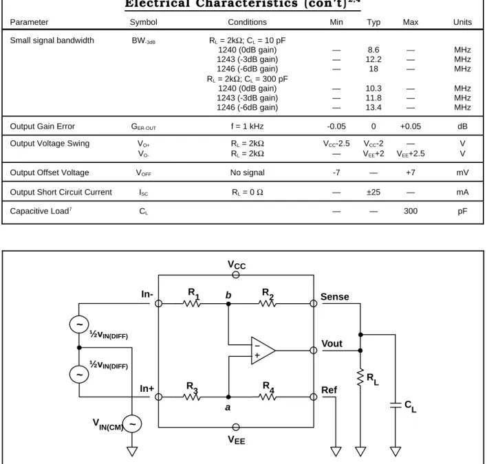
Sense
Vout
Ref
V
CCV
EEV
IN(CM)
In+
In-R
L
½v
IN(DIFF)~
~
~
b
a
C
L½v
IN(DIFF)Figure 2. THAT 1240 series test circuit
Theory of Operation
Therefore, to achieve this high CMRR in practice, care should be taken to ensure that all source impedances remain balanced. To accomplish this, PCB traces carrying signal should be balanced in length, connector resistance should be minimized, and any input capacitance (including strays) should be balanced between the + and - legs of the input circuitry. Note that the additional contact resistance of some sockets is sufficient to undo the effects of precision trimming. Therefore, socketing the parts is not recommended. THAT’s 1200-series InGenius® input stages address many of these difficulties through a patented method of increasing common-mode input impedance.
A further consideration is that after trimming, the two resistor divider ratios are tightly controlled, but the actual value of any individual resistor is not. In fact, two of the four resistors are normally left without trimming. The initial tolerance of the tors is quite wide, so it is possible for any given resis-tor to vary over a surprisingly wide range, Lot-to-lot variations of up to ±30 % are to be expected.
Input Considerations
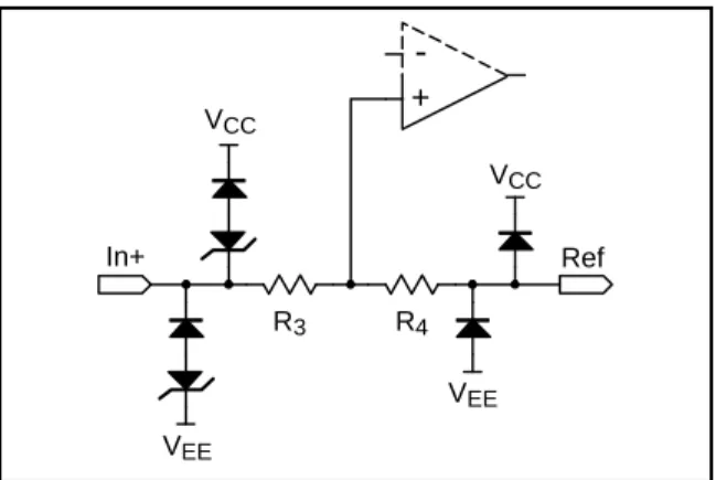
The 1240-series devices are internally protected against input overload via an unusual arrangement of diodes connecting the + and - Input pins to the power supply pins. The circuit of Figure 3 shows the arrangement used for the R3/R4 side; a similar one applies to the other side. The zener diodes prevent the protection network from conducting until an input pin is raised at least 50 V above VCC or below
VEE. Thus, the protection networks protect the
devices without constraining the allowable signal swing at the input pins. The reference (and sense) pins are protected via more conventional reverse-biased diodes which will conduct if these pins are raised above VCC or below VEE.
Because the 1240-series devices are input stages, their input pins are of necessity connected to the outside world. This is likely to expose the parts to ESD when cables are connected and disconnected. Our testing indicates that the 1240-series devices will typically withstand application of up to 1,000 volts under the human body ESD model.
To reduce risk of damage from ESD, and to prevent RF from reaching the devices, THAT recom-mends the circuit of Figure 4. C3 through C5 should be located close to the point where the input signal comes into the chassis, preferably directly on the connector. The unusual circuit design is intended to minimize the unbalancing impact of differences in the values of C4 and C5 by forcing the capacitance from each input to chassis ground to depend primar-ily on the value of C3. The circuit shown is approxi-mately ten times less sensitive to mismatches
between C4 and C5 than the more conventional
approach, in which the junction of C4 and C5 is grounded directly. An excellent discussion of input stage grounding can be found in the June 1995 issue of the Journal of the Audio Engineering Society, Vol. 43, No. 6, in articles by Stephen Macatee, Bill Whitlock, and others.
Note that, because of the tight matching of the internal resistor ratios, coupled with the uncertainty
in absolute value of any individual resistor, RF bypassing through the addition of R-C networks at the inputs (series resistor followed by a capacitor to ground at each input) is not recommended. The added resistors can interact with the internal ones in unexpected ways. If some impedance for the RF-bypass capacitor to work against is deemed necessary, THAT recommends the use of a ferrite bead or balun instead.
If it is necessary to ac-couple the inputs of the 1240-series parts, the coupling capacitors should be sized to present negligible impedance at any frequen-cies of interest for common mode rejection. Regard-less of the type of coupling capacitor chosen, variations in the values of the two capacitors, working against the 1240-series input impedance (itself subject to potential imbalances in absolute value, even when trimmed for perfect ratio match), can unbalance common mode input signals, convert-ing them to balanced signals which will not be rejected by the CMRR of the devices. For this reason, THAT recommends dc-coupling the inputs of the 1240-series devices.
Input Voltage Limitations
When configured, respectively, for -3 dB and -6 dB gain, the 1243 and 1246 devices are capable of accepting input signals above the power supply rails. This is because the internal opamp’s inputs connect to the outside world only through the on-chip resis-tors R1 through R4 at nodes a and b as shown in Figure 2. Consider the following analysis.
Differential Input Signals
For differential signals (vIN(DIFF)), the limitation to signal handling will be output clipping. The outputs of all the devices typically clip at within 2V of the supply rails. Therefore, maximum differential input signal levels are directly related to the gain and supply rails.
Common Mode Input Signals
For common-mode input signals, there is no output signal. The limitation on common-mode handling is the point at which the inputs are overloaded. So, we must consider the inputs of the opamp.
For common mode signals (vin(CM)), the common mode input current splits to flow through both R1/R2 and through R3/R4. Because vb is constrained to follow va, we will consider only the voltage at node a.
The voltage at a can be calculated as:
v
a=
v
IN(CM)R4
R3+R4
Again, solving for vIN(CM),
v
IN(CM)=
v
a R3+R4R4
For the 1240, (R3 + R4) / R4 = 2. For the 1243, (R3 + R4) / R4 = 2.4. For the 1246, (R3 + R4) / R4=3. Furthermore, the same constraints apply to va as in the differential analysis.
Following the same reasoning as above, the maximum common mode input signal for the 1240 is (2VCC - 4) V, and the minimum is (2VEE + 4) V. For the 1243, these figures are (2.4VCC - 4.8) V, and (2.4VEE + 4.8) V. For the 1246, these figures are (3VCC - 6) V, and (3VEE + 6) V.
Therefore, for common-mode signals and ±15 V rails, the 1240 will accept up to ~26 V in either direction. As an ac signal, this is 52 V peak-peak, 18.4 V rms, or +27.5 dBu. With the same supply rails, the 1243 will accept up to ~31 V in either direction. As an ac signal, this is 62 V peak-peak, 21.9 V rms, or +29 dBu. With the same supply rails, the 1246 will accept up to ~39 V in either direction. As an ac signal, this is 78 V peak-peak, 27.6 V rms, or +31 dBu.
Of course, in the real world, differential and common-mode signals combine. The maximum signal that can be accommodated will depend on the superposition of both differential and common-mode limitations.
Output Considerations
The 1240-series devices are typically capable of supplying 25 mA into a short circuit. While they will survive a short, power dissipation will rise dramati-cally if the output is shorted. Junction temperature
must be kept under 125 ºC to maintain the devices’ specifications.
These devices are stable with up to 300 pF of load capacitance.
Power Supply Considerations
The 1240-series parts are not particularly sensi-tive to the power supply, but they do contain wide bandwidth opamps. Accordingly, small local bypass capacitors should be located within a few inches of the supply pins on these parts, as shown in Figure 4.
Selecting a Gain Variation
The three different parts offer different gain structures to suit different applications. The 1246 is customarily configured for -6 dB gain, but by revers-ing the resistor connections, can also be configured for +6 dB. The 1243 is most often configured for -3 dB gain, but can also be configured for +3 dB. The choice of input gain is determined by the input voltage range to be accommodated, and the power supply voltages used within the circuit.
To minimize noise and maximize signal-to-noise ratio, the input stage should be selected and config-ured for the highest possible gain that will ensure that maximum-level input signals will not clip the input stage or succeeding stages. For example, with ±18 V supply rails, the 1240-series parts have a maximum output signal swing of +23 dBu. In order to accommodate +24 dBu input signals, the maximum gain for the stage is -1 dB. With ±15 V supply rails, the maximum output signal swing is ~+21.1 dBu; here, -3 dB is the maximum gain. In each case, a 1243 configured for -3 dB gain is the ideal choice. The 1240 (0dB gain only) will not provide enough headroom at its output to support a +24 dBu input signal. The 1246 (configured for -6 dB gain) will increase noise, thus reducing dynamic range, by attenuating the input signal more than necessary to support a +24 dBu input.
In fact, for most professional audio applications, THAT recommends the -3 dB input configuration possible only with the 1243 in order to preserve dynamic range within a reasonable range of power supply voltages and external headroom limits.
Figure 5. Zero dB line receiver
6
1 3
2
+In
-In 9k 9k 5
9k 9k
U1 1240
Output
7
4
Sense
Vout
Ref VCC
VEE
In+
In
-+
In+ Ref
VCC
VEE
VCC
VEE R3 R4
Figure 3. Representative input protection circuit
C4 470p
C5 470p C3
47p
In+
In-Out
C1
100n C2
100n VCC
VEE In-2
In+ 3
Out 6
U1
THAT1246/1243/1240
Ref Sens VEE
VCC 5
7
4 1
The THAT 1240, 1243, and 1246 are usually thought of as precision differential amplifiers with gains of zero, -3 and -6 dB respectively. These devices are primarily intended as balanced line receivers for audio applications. However, their topology lends itself to other applications as well.
Basic Balanced Receiver Applications
Figures 5, 6, and 7, respectively, show the THAT 1240, 1246, and 1243 configured as zero, -6 dB, and -3 dB line receivers. Figures 8 and 9, respectively, show the 1243 and 1246 configured as +3 dB and +6 dB line receivers. The higher gains are achieved by swapping the positions of the resistors within each pair in regard to signal input vs. output.
Figure 10 shows a THAT 1240 configured as a precision summing amplifier. This circuit uses both the In+ and Ref pins as inputs. Because of the excel-lent matching between the laser-trimmed resistor pairs, the output voltage is precisely equal to the sum of the two input voltages.
More Complex Applications
Figure 11 shows a 1240 configured as an instru-mentation amplifier. The two opamps preceding the 1240 provide gain equal to 1+(9.998 kΩ / Rg). The 1240 rejects common mode signals while accepting balanced ones.
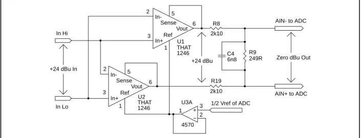
Figure 12 shows a convenient method of driving a typical audio ADC with balanced inputs. This circuit accepts +24 dBu in. By using a pair of THAT 1246 ICs connected in anti-phase, the signal level
between their respective outputs is +24 dBu. An attenuator network brings this signal down by 24 dB while attenuating the noise of the line receivers as well.
The output noise of a THAT 1246 is -106 dBu, and since there are two of them, the total noise level going into the resistive pad will be -103 dBu. The pad reduces the noise level to -127 dBu at the input to the ADC. The noise density resulting from the line receivers will therefore be
e
n line receiver=
10−127dBu
20 %0.775 20kHz
=
2.45
nV Hz
The thermal noise of the 249 Ω resistor is
2.05 nV/√Hz. We can assume that the noise contri-bution of R8 and R19 will be negligible, and therefore, the total noise density going into the input of the ADC will be
.
e
n total= (
2.45
nVHz)
2+ (
2.06
nVHz)
2=
3.2
nVHz The noise floor can then be calculated to beNoise
(dBu)=
20 log
3.2 nVHz % 20kHz
0.775
= −
124.7
dBu
Figure 13 shows the recommended method for controlling gain in a balanced system. In such circuits, designers are often tempted to keep the signal balanced and use two Voltage Controlled Amplifiers (VCAs) to independently control the gain on each half of the balanced signal. Unfortunately, this can result in common-mode to differential mode
Applications
6
1 3
2
+In -In
5
12k 6k
12k 6k
U1 1246
Output 7
4
Sense
Vout
Ref VCC
VEE
In+
In-Figure 9. +6 dB line receiver
6
1 3
2
+In -In
5 10.5k 7.5k
10.5k 7.5k U1 1243
Out 7
4
Sense
Vout
Ref VCC
VEE
In+
In-Figure 8. +3 dB line receiver
6
1 3
2
+In
-In 12k 6k 5
12k 6k
U1 1246
Output 7
4
Sense
Vout
Ref VCC
VEE
In+
In-Figure 7. -6 dB line receiver Figure 6. -3 dB line receiver 6
1 3
2
+In
-In 10.5k 7.5k 5
10.5k 7.5k U1 1243
Output 7
4
Sense
Vout
Ref VCC
VEE
In+
In-conversion (degrading CMRR) when there are even slight differences in gain between the VCAs. A better approach is to convert the signal to single-ended, alter the gain, and then convert back to balanced.
In Figure 13 we use a THAT 1243 -3 dB line receiver to do the balanced-to-single-ended conver-sion. The VCA section also has a static gain of -3 dB due to the ratio of R2 to R3. This circuit can accept
+24 dBu, since the THAT 1243 output stage is capable of accepting 21 dBu without distortion. Reducing R3 to 14 kΩ results in a 3 dB reduction in VCA output noise. This arrangement results in 3 dB greater dynamic range compared to the case where a -6 dB line receiver and a VCA with zero dB static gain are used. After the VCA, the signal is restored to 24 dBu by the THAT 1606.
6 Output
1 3
2
Input 1
Input 2
5
9k 9k
9k 9k
U1 1240
Sense
Vout
Ref VCC
VEE
In+
In-7
4
Figure 10. Precision two-input summing circuit
3 2
1
U2A OP-270B
5 6
7
U2B OP-270B R1
Rg R2 4k99
R3 4k99
In+
In-Out
C2
100n C1
100n VCC
VEE In-2
In+ 3
Out 6
U1 THAT1240
Ref Sens VEE
VCC 5
7
4 1
Figure 11. Instrumentation amplifier
Figure 12. Circuit for audio ADCs with balanced inputs In Hi
In Lo
AIN- to ADC
AIN+ to ADC R8
2k10
R9 249R
R19 2k10
C4 6n8 +24 dBu In
Vout 6 In+
3 In-2
U1 THAT 1246
Vout 6 In+
3 In-2
U2
3 2 1
U3A
4570
1/2 Vref of ADC
+24 dBu Zero dBu Out
Ref Sense
5
1
Ref Sense
5
1 THAT1246
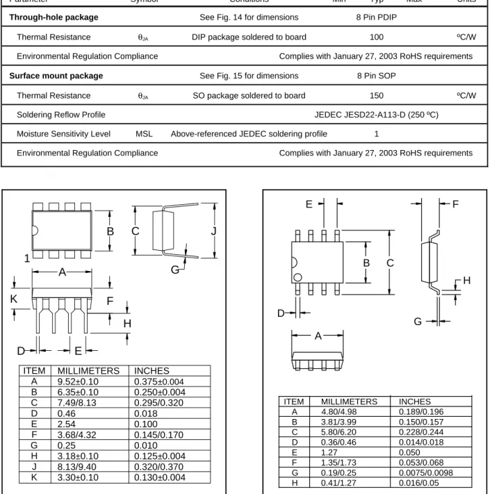
The THAT 1240 series is available in 8-pin PDIP and 8-pin surface mount (SOIC) packages. Package dimensions are shown below;
The 1240 series packages are entirely lead-free. The lead-frames are copper, plated with successive layers of nickel, palladium, and gold. This approach makes it possible to solder these devices using lead-free and lead-bearing solders.
Neither the lead-frames nor the plastic mold compounds used in the 1240-series contains any hazardous substances as specified in the European Union's Directive on the Restriction of the Use of Certain Hazardous Substances in Electrical and Electronic Equipment 2002/95/EG of January 27, 2003. The surface-mount package is suitable for use in a 100% tin solder process
Parameter Symbol Conditions Min Typ Max Units
Through-hole package See Fig. 14 for dimensions 8 Pin PDIP
Thermal Resistance θJA DIP package soldered to board 100 ºC/W
Environmental Regulation Compliance Complies with January 27, 2003 RoHS requirements Surface mount package See Fig. 15 for dimensions 8 Pin SOP
Thermal Resistance θJA SO package soldered to board 150 ºC/W
Soldering Reflow Profile JEDEC JESD22-A113-D (250 ºC)
Moisture Sensitivity Level MSL Above-referenced JEDEC soldering profile 1
Environmental Regulation Compliance Complies with January 27, 2003 RoHS requirements
Package Characteristics
Package Information
B
A
K
F
H
E
D
G
J
C
ITEM A B C D E F G H J K
1
MILLIMETERS 9.52±0.10 6.35±0.10 7.49/8.13 0.46 2.54 3.68/4.32 0.25 3.18±0.10 8.13/9.40 3.30±0.10
INCHES 0.375±0.004 0.250±0.004 0.295/0.320 0.018 0.100 0.145/0.170 0.010 0.125±0.004 0.320/0.370 0.130±0.004
Figure 14. -P (DIP) version package outline drawing
0.41/1.27
H 0.016/0.05
0.228/0.244
0.0075/0.0098 0.053/0.068 0.014/0.018 0.189/0.196 INCHES 0.150/0.157
G
H
F
C
B
D
F G D E A B C
ITEM MILLIMETERS
0.36/0.46
0.19/0.25 1.35/1.73 1.27 4.80/4.98 3.81/3.99 5.80/6.20
0.050