1
© Global Society of Scientific Research and Researchers
http://ijcjournal.org/
A New Reversible Design of Adder & Subtractor Using
Reversible Logic Gates
Sonawane Swati Shrinivas
a*, Proff. Vishal Puranik
baME ( E & T C ) Dept JSPM’s BSIOTR, Wagholi, Pune, India
b(E & TC) Dept JSPM’s BSIOTR Wagholi, Pune, India
aEmail: [email protected]
bEmail: [email protected]
Abstract
Modern VLSI design circuitry is used for low power consumption which is the requirements of ICs. Reversible logic has its tremendous applications and importance because it doesn’t lose any single bit of information of no information while performing computation bit loss during computation; it reflects the result in low power dissipation. However, we have to convert the reversible circuits into fault tolerant reversible circuits; it helps to detect the occurrence of errors and faults. Parity preserving property can be used for this. A new parity preserving reversible gate is proposed in this paper, named as P2RG. The most significant aspect of this work is that it can work as a full adder as well as full subtractor by using one P2RG and Fredkin gate only. This proposed design is very good in terms of gate count, garbage outputs, constant inputs and area than the existing similitude. The concept behind the reversible logic circuits is that the inputs and outputs are same.
Keywords: Fredkin Gate; Constant Inputs; Garbage Output.
1. Introduction
Modern VLSI design circuitry is used for low power consumption which the need of ICs the. Reversible logic has its strong applications because of no single information bit loss during computation [1]; therefore it consumes very less power. However, there is a demand to convert the reversible circuits into fault tolerant reversible circuits to identify the presence of errors. Parity preserving property can be used for this. A new 5*5 parity preserving reversible gate is proposed in this paper, named as P2RG.
---
2
The most valuable feature of this work is that it can work both as a full adder and a full subtract or by using one P2RG and Fred kin gate only. Proposed design is good when considering the factors like, gate count, garbage outputs, constant inputs and area than the existing similitude. Thus, this paper helps to understand the initial threshold to design more complex systems which will be able to execute more complicated operations using parity preserving reversible logic. The reversible logic circuit plays a very important role in modern VLSI circuit design. The Applications of this proposed architecture are quantum computers, low power CMOS designs, optical computing. It’s very important application is in nanotechnology. These are the most considerable applications of reversible logic circuits. There is a single logic gate, this gate is called reversible logic gate, and collection of large no. of reversible logic gates, if forms a one reversible logic circuit
2. Proposed system
Following figure shows the complete block diagram of proposed system. There are following no. of logic gates
• Feynman Gate
• Perse Gate
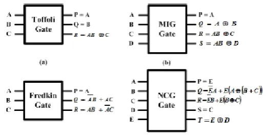
• Toffoli Gate
• Fredkin Gate
In this proposed structure, we are going to use Fredkin Gate.
In the implementation stage, we are going to design two types of circuts-
• Parity Preserving Half Adder/Subtractor
• Parity Preserving full Adder/Subtractor
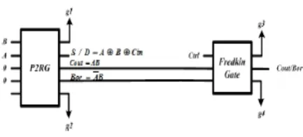
Figure 1: Parity Preserving half adder subtractor
3
incrementing and decrementing operations and similar kind of operations. Although adders can be used to represent many numerical representations, such as binary-coded decimal or excess-3, but the basic thing is that the most adders are work on an binary numbers. In binary digital, negative numbers are represented by using two's complement or ones' complement, it is curtail to modify an adder into an adder–subtractor. Other signed number representations require more logic around the basic adder.
Figure 2: Parity Preserving full adder subtractor
3. Fredkin gate
The figure shows the logical symbol of Fredkin Gate [2]. There are 3 inputs & 3 outputs. The inputs are A, B, C and the outputs are P=A, Q= A’B EXOR AC and R= A’C EXOR AB
Figure 3: (A) Toffoli Gate (B) MIG Gate (C) Fredkin Gate (D) NCG Gate
The concept behind that means reversible logic gate is that there is a one to one mapping means number of outputs equal to number of inputs. The very important gate is not gate. The Proposed concept will work as a adder as well as subtraction by using a single board. In parity preserving full adder and subtractor is realized or implemented by using P2RG gate one Fredkin gate. Reversible logic is characterized by the following parameters
1)There are equal number of inputs and outputs
4
4. ImplementationBelow is the Implementation of this proposed work.
A. Software Tools:
• Xilinx ISE 14.4
• Modelsim 6.1
B. Programming Languages:
• Verilog HDL
• VHDL
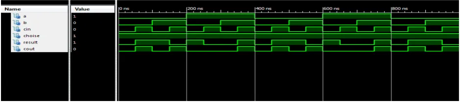
5. Simulation result
Figure 4: Architectural Schematic
Figure 5(a): Waveforms of Proposed work (Full Adder)
5
6. Constraints \ limitationsThe following are the important design constraints for reversible logic circuits.
• Reversible logic gates do not allow fan-outs.
• Reversible logic circuits should have minimum quantum cost.
• The design can be optimized so as to produce minimum number of garbage outputs.
• The reversible logic circuits must use minimum number of constant inputs.
• The reversible logic circuits must use a minimum logic depth or gate levels
7. Conclusion
In this proposed architecture, we show that reversible logic is very applicable because it saves the valuable information. In a digital world, every bit of information is very important. It saves much area on the chip itself, There are less number of garbage outputs.
8. Recommendation
In future, this design can be extended to 16, 32 and 64 bits. A reversible multiplier and divider can also be designed and included into this ALU. Moreover, this design may be extended to gate level implementation.
Acknowledgement
I am very thankful to Prof. Vishal Puranik for his valuable support and guidance for making this project successful.
References
[1]. R. Landauer, “Irreversibility and heat generation in the computing process,” IBM journal of research and development, vol. 5, no. 3, pp.183–191, 1961.
[2]. E. Fredkin and T. Toffoli, Conservative logic.Springer, 2002.