DESIGN AND IMPLEMENTATION OF FFT FILTER
USING VHDL IP CORE BASED DESIGN
1
Ravindra Kumar,
2S.K Sahoo,
3Balbindra Kumar
1
M.Tech(VLSI Design),
2Asst. Professor ,
3M.Tech(VLSI Design)
Noida Institute of Engineering & Technology, Knowledge park-III, Greater Noida, U.P (India)
ABSTRACT
The FIR FFT core is intended for the signal filtering. With the FIR filter of large impulse response length which
exceeds up to Ni = 512 samples. Each FFT iteration dates are computed by the computational unit, called
FFTDPATH, another words, data path for FFT calculations. FFTDPATH calculates the radix-2 FFT butterfly
in the high pipelined mode. Therefore in each clock cycle one complex number is read from the data RAM and
the complex result is written in this RAM. This mode supports the increasing the clock frequency up to 80 MHz
and higher. In the core the block floating point arithmetic is implemented. The system puts band pass filter and
one or two differentiators sequentially. The sectioned convolution algorithm is used for the one channel complex
signal filtering. The filtering of a single input signal is performed with the abundance of operations because the
imaginary part of the input data is zeroed. This abundance is minimized when the imaginary part of FFT is data
of another input signal (second channel).
Keywords—Component, Formatting, Style, Styling, Insert (Key Words)
I.INTRODUCTION
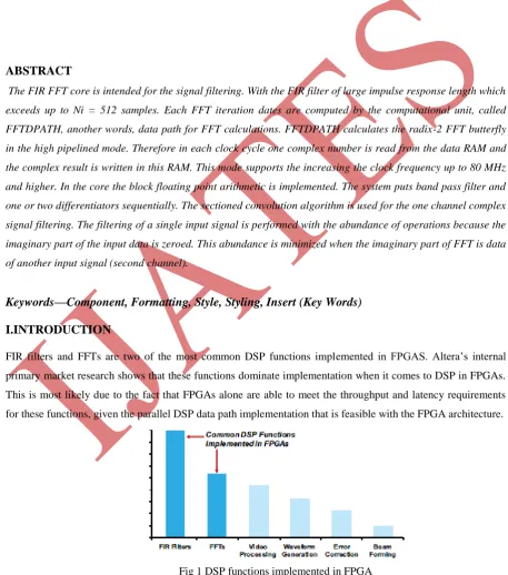
FIR filters and FFTs are two of the most common DSP functions implemented in FPGAS. Altera’s internal primary market research shows that these functions dominate implementation when it comes to DSP in FPGAs. This is most likely due to the fact that FPGAs alone are able to meet the throughput and latency requirements for these functions, given the parallel DSP data path implementation that is feasible with the FPGA architecture.
Given the preponderance of FIR and FFT implementation, it is critical that the FPGA DSP architecture be designed to enable this implementation with highest performance and the least resources. At the 28-nm process node, Altera has developed the FPGA industry’s first variable-precision DSP architecture in its Stratix® V
devices. This architecture enables designs with varying precision and performance requirements to be implemented using the 28-nm silicon fabric with two to three times the implementation efficiency compared to competing, fixed-precision 18x25 DSP architectures.
Digital filter plays an important role in digital signal processing applications. Digital filters are widely used in digital signal processing applications, such as digital signal filtering, noise filtering, signal frequency analysis, speech and audio compression, biomedical signal processing and image enhancement etc. A digital filter is a system which passes some desired signals more than others to reduce or enhance certain aspects of that signal. It can be used to pass the signals according to the specified frequency pass-band and reject the frequency other than the pass-band specification. The basic filter types can be classified into four categories: low-pass, high-pass, band-high-pass, and band-stop. On the basis of impulse response, there are two fundamental types of digital filters: Infinite Impulse Response (IIR) filters, and Finite Impulse Response (FIR) filters.
Finite Impulse Response digital filter has strictly exact linear phase, relatively easy to design, highly stable, computationally intensive, less sensitive to finite word-length effects, arbitrary amplitude-frequency characteristic and real-time stable signal processing requirements etc. Thus, it is widely used in different digital signal processing applications.
FIR filter is described by differential equation. The output signal is a convolution of an input signal and the impulse response of the filter.
1 0
( ) ( ( ) ( ))
N
k
y n h k X n k
(1)x(n) is the input signal. h(n) is the impulse response of fir filter.
The transfer function of a causal FIR filter is obtained by taking the z-transform of impulse response of FIR filter h(n).
1 0
( ) ( ) )
N
k k
H z h k z
(2)Most Common type filters include a low-pass filter, which pass through the frequencies below their cut off frequencies, and progressively attenuates frequencies above the cutoff frequency of a signal according to desired requirements. There are many straightforward techniques for designing FIR digital filters to meet arbitrary frequency and phase response specifications, such as window design method or frequency sampling techniques. The Window method is the most popular and effective method because this method is simple, convenient, fast and easy to understand. The main advantage of this design technique is that the impulse response coefficient can be obtained in closed form without the need for solving complex optimization problems.
window functions, for the fixed length the Rectangular window provides smallest main lobe width but the highest peak of side lobe among them, So Rectangular window is not widely used in digital signal processing applications. The Hanning and Hamming window provides good side lobe attenuation compare to rectangular window, so these windows are commonly used in different DSP applications. For higher side lobe attenuation Blackman window is used but the Blackman window has a wider main lobe width compare to Hanning and Hamming window. The Kaiser window is a kind of adjustable window function which provides independent control of the main lobe width and ripple ratio. But the Kaiser window has the disadvantage of higher computational complexity due to the use of Bessel functions in the calculation of the window coefficients. In some applications such as FFT, signal processing and measurement, higher side lobe attenuation is required compared to a Hamming window. The Blackman window function can also be used for these types of applications but the Blackman window has a wider main lobe width and if the main lobe width of any window function increases the ability to distinguish two closely spaced frequency components decreases.
An efficient adjustable window function based on Blackman window function is used for designing an FIR filter. For an efficient value of µ, this window function provides higher side lobe attenuation comparison to Hamming and Hanning windows and the main lobe width of this window function is slightly greater than the hamming window. In this window function for a fixed length the main lobe width and amplitude of side lobe can be varied in the frequency domain by changing the value of µ, which provides greater flexibility according to different applications. the design filter is compared for some different values of µ.
II. FEATURES OF FIR FILTER
The filtering algorithm is the sectioned convolution with accumulating based on N-point radix-2 FFT, where N = 64, 128, 256, 512, 1024.
One complex signal channel or two parallel real signal channels.
Filter types are LPF; LPF and HPF; LPF and HPF, and differentiator; LPF and HPF, and double
differentiator.
Input data, output data, and coefficient widths are generics.
Bandpass frequencies of the LPF and HPF filters, filter type are dynamically tunable parameters. The frequencies for both real channels are tuned independently.
Stop band ripple for 16-bit dates is higher than 60 db. The transitional frequency band is less than 6 bins
(1 bin = Fs/N, where Fs is the sampling frequency). Dynamic range for 16-bit dates is higher than 70 db.
Structure optimized for Xilinx Virtex2, Virtex4, Spartan3 FPGA devices, and can be implemented in
Altera, Actel, Lattice devices as well.
The maximum clock frequency for Virtex4_ devices is equal to Fclk = 190 MHz, and for Spartan3E
devices is equal to Fclk = 80 MHz.
2.1 Design features
2.2.1 Small hardware volume
The USFIR_FFT core is intended for the signal filtering with the FIR filter of large impulse response length which exceeds up to Ni = 512 samples. Consider the sequential-parallel FIR filter of the length Ni = 512 based on the DSP48 module of the Virtex4 device with the slow-down ratio 32. This ratio for USFIR_FFT core cannot be less than 29. Then the FIR filter hardware volume occupies 512/32 = 16 DSP48 modules and buffer RAMs. I.e. such a filter occupies in 4 times more DSP48 modules than the USFIR_FFT core does. Considering that the USFIR_FFT core has 2 parallel independed channels, the hardware volume effectiveness ratio increases to 8 times. Comparing to the Virtex2, and Spartan3 devices, the hardware volume effectiveness of the USFIR_FFT core is higher because the DSP48 modules are absent in them.
2.2.2 Dynamically tunable band pass frequency
In many applications the user needs the filters which band pass frequencies are tuned dynamically. They are adaptive filtering, software defined radio, ultrasound testing devices, etc. It is not easy problem to perform this mode in the usual FIR or IIR filters. This problem is usually solved by storing a set of coefficients of different filters or by calculating the new coefficient set each time on demand.
In the first situation the coefficient ROM has to be too large to provide the proper frequency tuning. In the second situation the calculating procedure is too complex to be performed in FPGA, and the tuning can waste too high time volume.
In the USFIR_FFT core the band pass frequencies are set simply as the codes of proper frequency bins. After new frequency setting the filter runs immediately, providing short and natural transitional process.
2.2.3 Highly pipelined calculation
Each FFT iteration dates are computed by the computational unit, called FFTDPATH, another words, data path for FFT calculations. FFTDPATH calculates the radix-2 FFT butterfly in the high pipelined mode. Therefore in each clock cycle one complex number is read from the data RAM and the complex result is written in this RAM. This mode supports the increasing the clock frequency up to 80 MHz and higher. [9]
2.2.4 High precision computation
In the core the block floating point arithmetic is implemented. This means that the data array has the common exponent, and the array is normalized in the mode when the maximum data in the array occupies all the digits of the word. Such mode supports the high calculation precision. Due to this mode, 1024 – point FFT calculations for 16 bit data and coefficients give 70 db signal to noise ratio, which is at least at 20 db higher than calculations with the fixed point arithmetic give[3][4].
2.2.5 Combining the band pass filter with differentiators
this situation the USFIR_FFT core is the best solution because this mode is implemented in it naturally without additional hardware.
2.2.6 Additional frequency measurements
Often the user needs to investigate the input signal spectrum, for example, to find out the noisy frequency bands. To implement this feature the USFIR_FFT core has additional output for signal spectrum samples or bins. This output is attached/detached on demand when instantiating the core[6][7].
III. FILTERING ALGORITHM
3.1 One channel real signal filter
The sectioned convolution algorithm is used for the one channel complex signal filtering. Consider N = 1024. This algorithm for convolution of the signal a with the impulse responce h looks like the following.
Input signal is divided into segments ak of the length 512.
The working array a of the length 1024 is formed as the concatenation of this segment and previous
one: a = <ak-1, ak >.
FFT of the length 1024 for the working array is implemented: A = F(a).
FFT of the length 1024 for the impulse responce is implemented: H = F(h); note that more than a half
of the array h has to be zeroed.
The signal spectrum and the impulse responce spectrum (frequency responce) are multiplied: A*H. Inverse FFT of the length 1024 is derived: y = F-1(A*H).
512 resulting samples are selected which are not inferred by the circular convolution effect: yk =
{yp,…, yp+511}, p = 256.
The following considerations have to be mentioned. The impulse response h may not be transferred into the frequency response H. Instead the frequency response H can be generated due the parameters of low pass frequency Fl and high pass frequency Fh. It has to be symmetric one and has more than 512 zeroed samples. The
initial algorithm is true for the signals, which are represented by the sum of sinusoids which periods are the fractions of the FFT period. If the signal is of common form then it could not be filtered precisely by this algorithm due to the frequency aliasing effect. To minimize this effect the
input signal has to be multiplied by some time window W. The resulting filtering algorithm for the real input signal is represented by the diagram on the Fig.3.3.1[8][9].
28-07-2014 - 04-08-2014
28-07-2014 - 04-08-2014
ak-1
yk
ak
511 0
0 511
W
0
Re Re Im Im
FFT
H
1023
Re Im
Re Im IFFT 0
0 256 767 511 y
3.2 Two filters for a single real signal
When filtering a single real signal with two different filters the input signal spectrum is just the same for both filters. But the frequency responce H2 of the second filter differs from the frequency responce H1 of the
first filter. To minimize the algorithm complexity the spectrum symmetry is used. If we have the real signal y1
with the spectrum (YR1 + jYl1) on the real input of FFT, and the real signal y2 with the spectrum (YR2 + jYl2) on
the imaginary input of FFT, then after FFT we get the spectrum:
YR = YR1 _ Yl2; (*)
Yl = Yl1 + YR2;
Therefore if the spectrum of both signals is forecalculated according to (*), then after IFFT we get one signal as the real part, and another signal as the imaginary part of the result. The resulting algorithm diagram is shown on the Fig.3.3.2.
28-07-2014 - 04-08-2014 ak-1 ak
511 0
0 511
W
0
Re Im
FFT Im Re
28-07-2014 - 04-08-2014 Interval Description
28-07-2014 - 04-08-2014 Interval Description H1
yk1
H2
Yk2
y1
y2
0 1023
0 1023
Re Re Im Im
IIFT
0
0 256
256 1023
1023 767
767
Fig.3.2.2 Algorithm of two filters for a single real signal 3.3 Two filters for two real signals
The filtering of a single input signal is performed with the abundance of operations because the imaginary part of the input data is zeroed. This abundance is minimized when the imaginary part of FFT is data of another input signal (second channel). I.e. the FFT input x is formed as:
x = a + jb, where
a = <ak-1 , ak >, b= < bk-1 , bk >.
After FFT the spectres of channels are restored from the spectrum X due to the formulas:
ARi = (XRi +XR(1024-i))/2;
Ali = (Xli – Xl(1024-i))/2;
BRi = (Xli +Xl(1024-i))/2;
Bli = - (XRi -XR(1024-i))/2; i=1,2,…,511;
AR0 = XR0;
BR0 = Xl0;
AR 512 = XR 512;
Al 0 = AR 512;
Bl 0 = BR 512;
Al 512 = 0;
Bl 512 = 0,
where R and l are indexes of the real and imaginary parts respectively. The rest of calculations is performed in the same manner as by the filtering of a single real signal by two filters.
3.2.4 Differentiating
The differentiating of the real signal is equival to multiplying its spectrum at the frequency w to the coefficient jw (-π <w <π). By the sectioned convolution it is enough to multiply the real part of the i-th spectrum bin to the coefficient i, and the imaginary part to the coefficient –i, and to swap them[10][11].
Time and frequency windows
Frequency window H derives the selective properties of the filter. The rectangle window gives the shortest transitional frequency band. But it is bad because its IFFT has not zeros, and therefore it causes the aliasing effect. In the USFIR_FFT core the Blackman window is used which has not ripples in the band pass, and provides the suppression range more than 70 db. The time window consists of three parts. The first ant the third parts represent the halves of the Hanning window, and the second part is equal to 1.
3.4 Interface symbol
CLK CE RST DATAE START FILTER(1:0) L1(n-1:0) H1(n-1:0) L2(n-1:0) H2(n-1:0)
DATAIRE(iwidth-1:0) DATAIIM(iwidth-1:0)
ADDRESS(n-1:0) DATAORE(owidth-1:0) DATAOIM(owidth-1:0) EXP(3.0) READY SPRDY WESP
SPRE SPIM SPEXP
Fig.3.3.1 illustrates USFIR_FFT core symbol 3.5 Signal description
The descriptions of the core signals and generics are represented in the table 3.1.
Table3.4.1 USFIR_FFT core signal description.
3.6 Data representation
Input and output dates are represented by iwidth and owidth bit two-th complement complex integers, respectively. The spectrum data block exponent is 4-bit positive integer e, and the spectrum result Y is equal to Y = Ym*2e, where Ym is the real or imaginary part of the spectrum data. The exponent is the same for each
sample of the result array. The code of the band frequency is equal to the bin number where the filter pass level is equal to –3 db. Codes L1, L2 have to be less than respective codes H1, H2. For instance, for Fs =2500 kHz,
N=1024, and LPF with the bandpass 400 kHz the code H1=164 because 400*1024/2500 =163.84. If L1 = 0 or L2
= 0 then the respective HPF is detached. [6]
3.6.1 Timing diagrams
On the fig. 3.6.1 the input signal timing diagrams are shown. At the start of the filter operation the signal START is inputted, which starts the core algorithm. The clock CLK frequency derives the throughput of the core. This throughput can be decreased by the periodic signal CE. And the throughput decrease rate (core activity) is equal to the rate of CE impulse width to this impulse period. In the usual mode CE=1.
START
CLK
DATAE
DATAIRE
DATAIIM
7530 7181 66B1
1D25 3875
Signal DATAE strobes the input dates and its frequency is equal to the sampling frequency Fs of the input signals DATAIRE and DATAIIM. Its width has to be equal to the clock signal period or the signal CE period. Signals DATAE, DATAIRE and DATAIIM have the setting time before the clock signal edge not less than 1 HC (is proved automatically by the synthesis).
By N = 1024 the sampling frequency Fs has to be in 29 times or more less than the clock frequency. By another values of N this ratio can be less than 29. The control signals FILTER, L1, H1, L2, H2 are sampled by the core control unit and must be stable for the period of 2N clock impulses after the impulse SPRDY.
The timing diagrams of the output signals DATAORE and DATAOIM are represented on the fig.3.6.2. The impulse READY shows the beginning of the array output from the inner buffer memory. The strobe DATAE points to the outer device the period when the output dates are ready to be latched.
CLK
READY
DATAE
DATAORE
DATAOIM
-5631
-2014 2242
12 6227
4929
Fig.3.6.2 Output signal timing diagrams by Fclk/Fs = 12
The input signal spectrum is outputted to the outputs SPRE, SPIM as the real and imaginary parts. The spectrum timing diagrams are shown on the Fig. 3.6.3. The impulse SPRDY shows the beginning of the spectrum array output. The signal WESP=1 shows the time period of this array output. The signal FREQ is equal to the bin number. Two spectres are outputted simultaneously. In even clock cycles the spectrum bins of the first channel are outputted, and in odd clock cycles the bins of the second channel do. Because the spectrum of the real signal is symmetric one then only the first half of the spectrum is outputted. The bins of the first channel are numbered by FREQ as 0,1,…N/2-1, and the bins of the second channel - N/2, N/2+1,…,N-1 . The signal SPEXP is equal
to the exponent of the spectrum array, which is common for all the bins of FFT for a single input array. To derive the correct fixed point value of bins they have to be shifted right to SPEXP bits.
SPRDY
WESP
CLK
SPRE
SPIM
FREQ
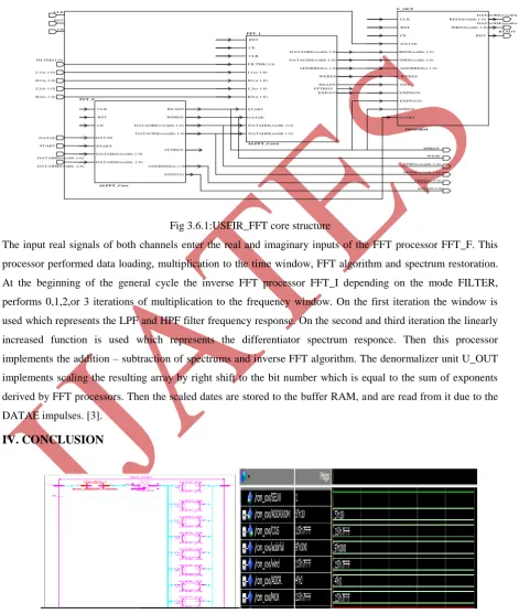
3.7 Core structure
USFIR_FFT core consists of the FFT processor (file ALFFT_Core_slip.vhd), IFFT processor (file ALFFT_Core_sli.vhd) and denormalizer (file DENORM.vhd) which are connected in a chain. The core structure is shown on the fig. 3.7
RST CE CLK FILTER(1:0) L1(n-1:0) H1(n-1:0) L2(n-1:0) H2(n-1:0) START DATAE DATAIRE(width-1:0) DATAIIM(width-1:0) DATAORE(width-1:0) DATAOIM(width-1:0) ADDRRES(n-1:0) WERES READY FFTRDY EXP(0.0) FILTER(1:0) L1(n-1:0) H1(n-1:0) H2(n-1:0) L2(n-1:0) DATAE START DATAIRE(iwidth-1:0) DATAIIM(iwidth_1:0) CLK RST CE CLK RST CE DATAE START DATAIRE(iwidth-1:0) DATAIIM(iwidth_1:0) READY WERES DATAORE(owidth-1:0) DATAOIM(owidth-1:0) FFTRDY ADDRRES(n-1:0) EXP(0.0) CLK RST CE DATAE REDI(width-1:0) IMDI(width-1:0) ADDRRES(n-1:0) WERES INIT EXPI(0.0) EXPF(0.0) SPRDY START REDO(width-1:0) IMDO(width-1:0) RDY DATAORE(owidth-1:0) DATAOIM(owidth-1:0) READY SPRDY WESP SPRE(owidth-1:0) SPIM(owidth-1:0) FREQ(n-1:0) SPEXP(3.0) FFT_F ALFFT_Core ALFFT_Corei FFT_1 U_OUT DENORM
Fig 3.6.1:USFIR_FFT core structure
The input real signals of both channels enter the real and imaginary inputs of the FFT processor FFT_F. This processor performed data loading, multiplication to the time window, FFT algorithm and spectrum restoration. At the beginning of the general cycle the inverse FFT processor FFT_I depending on the mode FILTER, performs 0,1,2,or 3 iterations of multiplication to the frequency window. On the first iteration the window is used which represents the LPF and HPF filter frequency response. On the second and third iteration the linearly increased function is used which represents the differentiator spectrum responce. Then this processor implements the addition – subtraction of spectrums and inverse FFT algorithm. The denormalizer unit U_OUT implements scaling the resulting array by right shift to the bit number which is equal to the sum of exponents derived by FFT processors. Then the scaled dates are stored to the buffer RAM, and are read from it due to the DATAE impulses. [3].
IV. CONCLUSION
We have implemented and verified the filtered algorithm with accumulating based on N-point radix-2 FFT with one complex signal channel or two parallel real signal channels. The filter types used are LPF and HPF and double differentiator. The bandpass frequencies of the LPF and HPF filters, filter type are dynamically tunable. The fft fir filter is implemented in the devices with Xilinx Virtex2TM, Virtex4TM, Spartan3TM.The maximum clock frequency for Virtex4TMdevices is equal to Fclk = 190 MHz, and for Spartan3E devices is equal to Fclk = 80 MHz. In the testbench the USFIR_FFT core is instantiated as the component in the standard instantiation. The core inputs the sine and cosine waves are put with the given frequency which is exchanged in time by the linear law. From the core outputs the results are sampled and analyzed.
REFERENCES
[1] Deepa Yagain, ―FIR Filter Design Based on Retiming & Automation Using VLSI Design Metrics‖ Technology, Informatics, Management, Engineering, and Environment (TIME-E), 2013 International Conference on ©2013 IEEE.
[2] Zheng Gao, ―A Study on Influence of Frequency Domain Constraint in FFT-based FIR Filter Design‖ Engineering and Technology (S-CET), 2012 Spring Congress on ©2012 IEEE.
[3] Rongxin Qu, ―High Performance Finite Impulse Response Filter on Graphics Processors‖ Intelligent Control and Information Processing (ICICIP), 2012 Third International Conference on ©2012 IEEE.
[4] D. Sova, ―Fault Tolerant Transform Domain Adaptive Noise Canceling from Corrupted Speech Signals‖ Circuits and Systems (MWSCAS), 2012 IEEE 55th International Midwest Symposium on ©2012 IEEE.
[5] Gang Liu, ―Design of Digital FIR Filters Using Differential Evolution Algorithm Based on Reserved Genes‖ Evolutionary Computation (CEC), 2010 IEEE Congress on ©2010 IEEE.
[6] R. Mahesh, ―New Reconfigurable Architectures for Implementing FIR Filters with Low Complexity‖ IEEE TRANSACTIONS ON COMPUTER- AIDED DESIGN OF INTEGRATED CIRCUITS AND SYSTEMS, VOL. 29, NO. 2, FEBRUARY 2010 ©2010 IEEE.
[7] Xi Zhang, ―Design of FIR Halfband Filters for Orthonormal Wavelets Using Remez Exchange Algorithm‖ IEEE SIGNAL PROCESSING LETTERS, VOL. 16, NO. 9, SEPTEMBER 2009 © 2009 IEEE.
[8] Evangelos F. Stefatos, ―Low-Power Reconfigurable VLSI Architecture for the Implementation of FIR Filters‖ Parallel and Distributed Processing Symposium, 2005. Proceedings. 19th IEEE International
[9] Timothy N. Davidson, ―Linear Matrix Inequality Formulation of Spectral Mask Constraints With Applications to FIR Filter Design‖ IEEE TRANSACTIONS ON SIGNAL PROCESSING, VOL. 50, NO. 11, NOVEMBER 2002 ©2002 IEEE.