MATERIALS
FOR KEY
This report is the result of a joint effort of the European Materials Research Society (E-MRS, Strasbourg, www.european-mrs.com) and of the Materials Science and Engineering Expert Committee (MatSEEC) of the European Science Foundation (ESF, www.esf.org/matseec). The report has been prepared on the occasion of the Key Enabling Technologies (KETs) initiative launched by the European Commission to give an overview of the current status and recommendations on the role Materials Science and Engineering should play in Europe for key enabling technologies. The report has been edited by Hans Richter, Vice-President of E-MRS, based on the contributions of several members. Thanks are due to Ana Helman, scientific secretary of MatSEEC, Manfred Aigringer, project manager of Gesellschaft zur Förderung von Wissenschaft und Wirtschaft (GFWW), Hilary Crichton (ESF), and John R. Blizzard (E-MRS) for performing the final compilation, editing and reviewing work.
Francesco Priolo Guenther Bauer
E-MRS President MatSEEC Chair
21 June 2011 – Second edition
Edited by: H. Richter,
E-MRS Vice-President
With the collaboration of:
N. Alford, J. Amouroux, D. Barbier, G. Bauer, A. Borg, J. P. Condé, A. González-Elipe, H. G. Grimmeiss, A. Jäger-Waldau,
D. J. Jarvis, T. Lippert, S. Maier, H. J. Muessig, E. Olsson, J. Perriere, L. Pfitzner, F. Priolo, H. Richter, A-C. Ritschkoff, P. Siffert, A. Slaoui, C. Vahlas
CONTENTS
1. Executive Summary 3
2. The Global Market and the EU Position for each KET 5
3. Advanced Materials 7
3.1 Research on New Advanced Materials with Novel or Improved Properties 7 3.2 Development of Rational Approaches in the Design of Advanced Materials 8
or in their Integration into Structures and Systems
3.3 Inspiration by Nature: Promotion of Eco-Design, of Bio-Inspiration 8 and of the Use of Natural Materials
3.4 Anticipation and Control of the Performance of Materials during their Life Cycle, 9 including Smart Structures allowing for Self-Sensing and Self-Healing
3.5 Advanced Functional Materials 10
3.5.1 Prospects of Inorganic Materials for Photonics and Energy 10
3.5.2 Prospects of Non-organic Materials for Advanced 10
Multifunctional Microsystems
3.5.3 Materials based on Novel Functional Low Molecular 10 Organic Compounds and Polymers
3.5.4 Metamaterials and Nanostructured Materials 10
3.5.5 Functional and Multifunctional Oxide Films 11
4. Materials for Energy 12
4.1 Energy Sources and Production 12
4.1.1 Solar Energy 13
4.1.2 Biomass 15
4.1.3 Thermo-Electric Energy 15
4.1.4 Nuclear Energy 16
4.2 Energy Storage and Distribution 17
4.2.1 Li-Ion Batteries 17
4.2.2 Supercapacitors 17
4.3 Carbon Dioxide as a Raw Material and a Future Chemical Fuel 18 for a Sustainable Energy Industry
4.3.1 General Objectives 18
4.3.2 How does this Process work? 18
4.3.3 Applications 18
4.3.4 Key Steps for a Development based on CO2 Valorisation 19
4.3.5 World Wide Equipment under Construction 20
4.3.6 Safety and Sustainability of the Process 20
4.3.7 Economical Impact 21
4.3.8 Conclusion 21
4.4 Energy Conversion 21
4.4.1 Fuel Cells 21
4.4.1.1 Polymer Electrolyte Fuel Cells 22
5.1 Materials and Fabrication 24
5.1.1 Top-down 24
5.1.2 Bottom-up 24
5.1.3 Nanotechnology for Energy 25
5.1.4 Nano-Bio Applications 26
5.1.5 Nanocomposites 26
5.2 Characterisation 26
5.3 Theory and Simulation 27
5.4 Summary and Recommendations 27
6. Materials for Micro-, Nanoelectronics and Silicon Photonics 28
6.1 Micro- and Nanoelectronics 28
6.1.1 “More of Moore” 30
6.1.2 “More than Moore” 30
6.1.3 Packing Density 31
6.1.4 Complexity 31
6.1.5 Multifunctionality 32
6.1.6 Signal Processing Rate 33
6.2 Carbon based Nanostructures 33
6.3 Micro- and Nano Electro-Mechanical Systems Technology (MEMS and NEMS) 35
6.4 Power Electronics 36
6.5 Silicon Photonics 37
6.5.1 Present Status 38
6.5.2 Future Trends 39
6.6 Conclusions and Recommendations 39
7. Biotechnology 40
8. General Conclusions 42
9. Authors 44
10. Sources 45
11. Appendix 47
1. EXECUTIVE SUMMARY
materials and material combinations are needed, but also their structural and electronic proper-ties have to be understood and optimised. As an example, we mention wind turbines, which have to have proper fracture strength and toughness in addition to superior aerodynamic properties. It is suggested that the electric energy produced by these novel techniques should be mainly stored as electrochemical energy. For such storage devices catalytic reactions and thus surface and interface phenomena play a key role. Carbon dioxide is seen as providing new opportunities for the develop-ment of an innovative industry capable of large energy storage by replacing carbon fossil fi elds.
Our daily life is now no longer imaginable without facilities like lap-top computers, mobile phones, smart-phones, etc. However, all these depend on batteries for the delivery of electric energy. Though the most powerful are Li-ion bat-teries they nevertheless sustain only a certain number of loading cycles before they fail due to thermal expansion during loading. Better elec-trodes for such batteries are therefore urgently needed. There are good reasons to believe that these improvements will be due to nanotechnology.
Micro- and Nanoelectronics is without any doubt the key enabling technology. Due to the tech-nological and economic importance of electronics, almost all industrial areas depend to an increasing extent on the progress of electronics. Data stor-age, data transfer and telecommunication are only a few examples. But areas such as control appli-cations in production facilities of automotive and aerospace space industries as well as household appliances, etc. need micro- and nanoelectronics for their functioning too. It is also worth men-tioning that with shrinking dimensions of basic elements, quantum mechanical phenomena will play an increasing role, and must be considered when designing future electronic devices.
Europe and the entire world face a number of chal-lenges which call for both immediate as well as medium term actions. The European Commission has identifi ed these problems and has suggested focussing, within the upcoming Common Strategic Framework for EU Research and Innovation funding, on initiatives which will strengthen in par-ticular innovation aspects. A number of so-called key enabling technologies which are of paramount importance to achieve the goals for strengthen-ing innovation in Europe have been identifi ed. At the same time it is clear that true innovation is often based on basic research and thus a strong research base has to be maintained and further developed in Europe.
The key enabling technologies (KETs) rec-ommended are: Advanced Materials, Photonics, Nanotechnology, Biotechnology, and Micro-and Nanoelectronics and, as a cross-cutting KET, Advanced Manufacturing Systems. These KETs are not only interlinked but are all based on further progress in materials development. Thus materi-als science and engineering plays a crucial role.
The fi eld of Photonics is another area, which is considered to become a mainstream technol-ogy of the 21st century. Photonic elements, which
convert electric signals into light and back into electric signals, are nowadays used e.g. for data transfer over long distances. In the future they will also be used for short distance data transmission e.g. within circuit boards and processors, and will thus in this way increase the data transfer rates within the Terabit/s range. Furthermore, apart from information and communication, photonics will change electric lighting as well due to the increasing use of light emitting diodes. Moreover, photonics has an enormous potential for indus-trial manufacturing through the use of high power lasers, and will have a strong impact on life and health sciences.
Biotechnology is another rapidly expanding fi eld with great impact on areas such as health-care, where targeted drug delivery is one of the aims, or for daunting analytic tasks like single molecule analysis. This fi eld will benefi t from recent advances in nanotechnology such as lab-on-a-chip systems, which can analyse with micro-fl uidic methods and sensors consisting, for example, of nanowires by using much less avail-able volumes than conventional techniques. In addition, nanostructured sensors will be a great deal more sensitive than bulk sensors because of their much larger surface/volume ratio.
In the following chapters a detailed analy-sis of the fi ve KETs and their role in solving the main challenges is presented by starting with an analysis of the present situation and then follow-ing up with suggestions and an outlook for the future. Below, we summarise a number of key recommendations:
• In some areas of micro- and nanoelectron-ics (MNE) Europe is still leading. Among those are power electronics, high frequency devices, and micro and nano-electromechanical sys-tems (MEMS and NEMS). In order to keep and strengthen this position it is of utmost impor-tance that a proper wafer production is available in Europe. All possible efforts must be made to take part in the upcoming transition to a technol-ogy based on 450 mm wafers and not to restrict future activities to centres and companies per-forming design and simulation only.
• Europe is leading in computational materials science worldwide. State-of-the-art multi-scale modelling of the relation between microstruc-ture and properties is needed both for the
understanding as well as the design of different types of advanced materials. Modern predictive materials modelling will be of key importance for European industry and in this respect the technology transfer to industry needs to be vig-orously pursued.
• In the fi eld of advanced materials it will be nec-essary to strengthen approaches to the rational design and characterisation of advanced mate-rials and their integration into structures and systems. It is therefore imperative to further support the expertise gained in hybrid materi-als, to integrate concepts of green chemistry and biotechnology in materials design, characterisa-tion and production, and to anticipate and control better the performance of materials during their entire life cycle.
• Due to promising applications in the fi eld of nano-technology it is mandatory to further develop this technology in areas such as energy, nano-bio applications, healthcare, security, etc in Europe. • In order to exploit fully the breakthroughs offered by nanotechnology a European open access centre for nanofabrication should be created offering state-of-the-art materials processing and characterisation facilities with strong links to industry.
• Carbon dioxide can be used as a raw material for electrical grid regulation and for the devel-opment of a new industry based on its recycling. In order to do this close cooperation between research centres and industries on this issue should be facilitated.
In conclusion, this document also underlines the necessity to strengthen innovation in Europe by
2. THE GLOBAL MARKET
AND THE EU POSITION FOR EACH KET
The history of science contains many examples showing how important it is for researchers to have strong will and perseverance in order to achieve the objectives they have set themselves. This is particularly true of materi-als science in view of the fact that material science and engineering is a multidisciplinary area that strongly interacts with technology. Materials science and engi-Materials science and engi-neering is also a well-recognised discipline with its dual grounding in basic science and engineering. As such, it plays a crucial role in many aspects of human activity including interactions with living environments and communication. Materials science develops new-gen-eration energy technologies such as solar cells, as well as providing faster and more reliable means of commu-nication through new electronic, optical, and magnetic materials.
It comes as no surprise then, that the history of materials science is highlighted by existing and often unexpected developments, which were not foreseen, for example, by classical roadmaps.
Following a process that identified the Key Enabling Technologies (KETs) from the European perspective, the European Commission set up a High Level Group that officially started its work on July 13, 2010 focussing on the five KETs which have a high impact in terms of mar-ket size and growth potential /refs EC1, EC2/.
• Nanotechnology has a global market estimated at US$ 147 bn in 2007 with the prediction to grow, in most optimistic assessments, to US$ 1 or even 3 trillion by 2015. The market share is dominated by the US (40%), followed by Europe (31%).
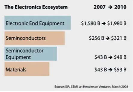
• Micro- and Nanoelectronics worldwide market was valued at US$ 261 bn in 2008. Electronic data processing and the telecommunication sector are the largest markets for microelectronics. However, semi-conductor components are rapidly penetrating the automotive, medical, industrial or consumer markets. The automotive sector in Europe accounts for a larger
proportion of microelectronics sales (19%) than it does in the rest of the world as a whole (8%).
• Photonics global market for optoelectronic compo-nents was worth US$ 356 bn in 2008 and is expected to grow at an annual rate of 3.1% up to 2020.The EU has strong positions in many photonics applications such as solid state lightening (e.g. LED), solar cells and laser assisted manufacturing.
• Advanced Materials and materials innovations are an important element in practically all manufacturing industries. Markets are expected to offer an additional volume within the EU of € 55 bn over the next 5 to 7 years with considerable potential in the areas of energy (€ 19 bn), environment, health, transport and informa-tion and communicainforma-tion technologies (ICT).
• Industrial biotechnology is defined as the applica-tion of biotechnology for the industrial processing and production of chemicals, materials and fuels. The global enzyme market was worth about € 2.1 bn in 2008 and Europe is the world leader in key indus-trial technologies such as enzyme technologies and fermentation.
Figure 2.2:
The Photonics Ecosystem
Figure 2.1:
Progress achieved in most technologies is closely related to progress in advanced materials. Examples, with differ-ent though systematically significant impact on societal needs, are energy related technologies (production, management such as lighting or heat conversion, stor-age and transformation), health technologies (including biomaterials and substitution devices), industries of the (micro-)electronic sectors, transportation (especially automotive and aeronautic), space, housing and civil engineering, production and construction technolo-gies in general, sport and clothing. This relationship results from the nature of materials science, an inherent interdisciplinary field, coupling fundamental research with engineering, and within which base knowledge is intimately related with technology. It is also the output of progress made in physics, chemistry and engineer-ing, and particularly because of the interactions among these three large sectors.
In the long term, four main directions should be supported because they correspond either to radically novel approaches in advanced materials design or to a societal expectation. These four directions potentially concern all classes of materials and are:
• Research on new advanced materials with novel or improved properties.
• Development of rational approaches in the design of advanced materials or in their integration into struc-tures and systems.
• Inspiration by nature: promotion of eco-design, bio-inspiration and the use of natural materials.
• Anticipation and control of the performance of mate-rials during their life cycle, including smart structures allowing for self-sensing and self-healing.
3.1 Research on New Advanced Materials with Novel or Improved Properties
In all industrial sectors, it is necessary to incorpo-rate new functionalities into “classical” materials (e.g.
ceramics, metals, textiles, paper, building and con-struction, etc.) to give them a higher added value. One example is single-crystalline materials with controlled defects. However, beyond such incremental, though necessary, progress, spectacular advances have been reported over recent years on the discovery of materials with new functionalities and/or with a wide spectrum of properties induced by the nanostructuring of mat-ter. Such new families include hybrid materials at the frontier between organic, bio- and inorganic worlds; divided solids with large specific surface areas, includ-ing mesoporous materials; novel carbon materials; memory shape materials; metamaterials, etc.
Many of these materials with specific properties condition the tuning and the breakthrough of innova-tive applications: membranes for separation processes, organic or thin film photovoltaics, functional poly-mers for flexible electronics, materials and devices for molecular photonics and photostable storage, thermo-electric materials at high and medium temperature, super isolating materials, cores of fuel cells, electrodes for all-solid batteries, molecular footprint materials, barrier polymers for packaging, shock resistant poly-mers, intermetallics with magnetic, electric, thermal, surface properties. These materials are particularly interesting for their combination of properties: com-plex metallic alloys, multiferroics, thermochromes, magnetochromes, etc.
In addition to the development of “materials for…” (a specific application), research on entirely new materi-als should be maintained and further developed. Recent examples are the iron based pnictides to be used as high temperature superconductors, developed in Japan. /ref KAM/.
The aim of this activity is to design and to syn-thesise or to process new phases and novel atomic architectures to be used as an upstream reservoir which will feed future families of “materials for…”. The follow-ing recommendations are provided:
• Encourage, maintain and recognise upstream activities on the synthesis of new compounds, complementary to the activities on materials for targeted applications • Develop adapted processes for the fabrication of such
materials
• Bring to the knowledge of industry the original devel-opments in the field of new compounds (to become new materials) which by nature are not yet included in industrial development
3.2 Development of Rational Approaches in the Design of Advanced Materials or in their Integration into Structures and Systems
Materials have long been simply transformed mat-ter which should fulfil a main required function. Future materials and/or material systems should fulfil multi-criteria specifications and therefore they will be multifunctional. Multifunctionality is often obtained from the coexistence within the material of a set of properties which are distributed at different scales. Such evolution of materials research towards an optimised design on demand is a new challenge which cannot be faced by using a blind process. It can only be achieved through:
(i) detailed insight into the mechanisms which control the properties,
(ii) a priori modelling of the expected properties, (iii) the systematic use of the possibilities offered by the
combination of different classes of materials, (iv) consideration of the potential presented by the
vari-ety of forms and architectures of a material, and (v) the adjustment of the properties of the interfaces.
This new challenge will also require the develop-ment of new techniques for materials processing or shaping and for disassembling in order to improve recycling.
Some industries, e.g. transportation, require technologi-cal breakthroughs; based on equivalent performance, they would allow structures’ weight reduction and extension of lifetime in specific operating conditions. In contrast, other sectors like the one of production of energy require devices that can operate in more severe conditions, under complex dynamic loading, under pressure or in vacuum, at high temperature or in cryo-genic cooling, in corrosive atmosphere, etc. In these
sectors in particular it is important to favour research in metallurgy taking into account expressed needs in the field of production of electricity by nuclear power.
When advanced materials are to be integrated into devices, such integration should be optimised considering interrogation and detection procedures, manufacturing and processing in given forms, and integration with other materials.
The following recommendations are provided: • Develop new approaches in materials design
• Develop the use of “numeric material” and confront the approaches developed for different classes of materials
• Develop integration processes/systems for successful and profitable use of the material’s functionalities • Develop instrumentation for materials
characterisa-tion: micro- and nanostructure, properties and per-formance in anticipated operating conditions. Include techniques for the in situ characterisation of materi-als during their processing and the continuation of the development of knowledge and of the use of large equipment (neutrons, synchrotron radiation) • Reinforce research at the interface among materials
chemistry, materials physics and engineering
3.3 Inspiration by Nature: Promotion of Eco-Design, of Bio-Inspiration and of the Use of Natural Materials
This direction corresponds both to radically novel approaches in advanced materials design and to a societal expectation. It promotes inspiration from natural materials and from processes nature uses for their fabrication. Efficiency of such materials, such as bone or wood, is based on their topological and structural organisation (hierarchy) at different scales: nanometre, micrometre and, most often, millimetre. Consequently, the objective is to design and to develop materials or components by modifying architecture, topology and length scales so as to give them the required functionalities.
The following recommendations are provided: • Better integrate the concepts and the objectives of
green chemistry and white biotechnology in materi-als design
• Optimise processes for the fabrication of materials and life cycle of systems
• Build alternatives to materials produced from raw materials with reduced availability
• Integrate a systemic approach in the design of new products, taking into account environmental and soci-etal aspects
• Research processing technologies for large diffusion materials like plastics, compatible with the objectives of sustainable development
3.4 Anticipation and Control of the
Performance of Materials during their Life Cycle, including Smart Structures allowing for Self-Sensing and Self-Healing
Society legitimately imposes a high security level for all devices used by mankind. This requires being able to understand and control the behaviour of the mate-rials used during their lifetime. Controlling matemate-rials lifetime involves three important aspects:
• Adjustment of a materials’ lifetime to its usage. Materials should be designed in such a way that their cost is adapted to the needs and particularly to the lifetime of the device which they are part of. Also the amount of used materials should be mitigated and materials should be recycled according to sustain-ability and efficiency principles.
• Prediction of the behaviour of the materials in dura-tions which are experimentally inaccessible. This question concerns an increasing number of applica-tions, especially in aeronautics and nuclear energy. It requires developing modelling and simulation tools which are able to provide complementary information to accelerated experiments, when possible.
• Determination of the remaining lifetime (remaining potential) as a function of the aging process experi-enced by the material during its use. It is convenient here to distinguish between batches of pieces, and sys-tems and structures. In the first case, the evaluation is realised a priori by statistical analysis, the distribu-tion width of which should be reduced. In the case of systems and structures it is necessary to dispose of non-destructive control coupled with identification models and precursor events. Precursor events are to be introduced in parts where aging signs are easily identified and quantified as, for example, in intelli-gent structures.
The following recommendations are provided:
• Observe and detect aging. Develop instrumentation, measurement facilities, probabilistic approaches, sto-chastic processes of deterioration
• Design smart structures allowing for self-sensing (warning) and self-healing; integrate these concepts together with those of sensors and actuators within the same material
As in the case of the four other KETs, new advanced materials should be processable in the targeted forms. To achieve this, it is mandatory that progress in mate-rials design with regard to more complex and strict specifications should be completed by both new and improved production technologies. Such technologies, incorporated in production lines, should particularly aim at reducing the production costs (e.g. by net shap-ing); at maintaining and if possible at decreasing the energetic cost; and at minimising the impact on the environment (e.g. by favouring low temperature and solvent-free synthesis). Such new and improved pro-cessing technologies may incorporate lasers, plasmas, ultrasounds, supercritical fluids, soft chemistry, spark plasma sintering or surface treatments. Up scaling of these processing technologies for mass production is another important issue in this respect: laboratory scale processing techniques should be designed in view of the pilot scaling.
In some cases, process intensification and security requires down scaling and parallel operation.
The parameters of a fabrication process are numer-ous and often coupled among them. The investigation of their influence requires extensive experimentation. Modelling, simulation and high throughput (e.g.
combinatorial) tools are strong supports for such devel-opments. It should be recalled that development of new synthesis/manufacturing equipment requires consider-able funding. This funding necessity should be satisfied as is the case of funding for large facilities for char-acterisation and testing (synchrotron, neutrons, etc.).
The following recommendations are provided: • Improve existing, and develop new processing,
assem-bling and transformation technologies adapted to the manufacturing of advanced materials and to their incorporation into systems
• Design laboratory scale processing techniques in view of the pilot scaling
• Integrate processing aspects in materials design and selection
All materials involved in the above items should contrib-ute to sustainabledevelopment. This will be achieved by applying life-cycle design of end products aimed at reducing environmental impact. In addition to the pre-viously presented requirements, reduced environmental impact is obtained from materials that contain abundant, accessible and less hazardous substances and present high resource productivity and low ecological rucksack.
3.5 Advanced Functional Materials
3.5.1 Prospects of Inorganic Materials for Photonics and Energy
In order to improve already existing and develop new inorganic materials for applications in photonics and nanotechnology, the current research trends in materi-als science include the following topics:
• Fast processes in oxide nanocrystals • Materials for holographic recording
• Detection of near-surface electromagnetic fields by optical resonances in atoms
• Optical properties, in particular, luminescence of wide band gap semiconductors
• Materials for electrodes and membranes for high stor-age capacity batteries and gas sensors
• Glasses for photonics
• Optical fibres and glasses for deep-ultraviolet applications
3.5.2 Prospects of Non-organic Materials for Advanced Multifunctional Microsystems
Both optoelectronic and micro- and nanoelectronic devices are priority in technology development. In order to develop the next generation of multifunctional advanced systems complex knowledge of physical and chemical properties of materials as well as of biological principles is required. The goal is to research relevant optical, electrical and micromechanical properties of materials. The results expected will create fundamental knowledge of the local atomic and electronic structure and its relation to physical and chemical properties of modern multifunctional materials including:
• Possibilities to use surface and interface processes in mono- and multilayer nanostructures for a new generation of surface-active sensors and ultrahard coatings
• Development of light emitters, detectors and visualisa-tion systems on oxyfluoride nanocomposite bases with enhanced quantum efficiency
3.5.3 Materials based on Novel Functional Low Molecular Organic Compounds and Polymers
The goal is to develop novel photoactive organic compounds (oligomers and polymers) and solid state systems for electronics, photonics and optoelectronics. The aim of investigations should be to demonstrate the integration of organic molecules, polymers or nanopar-ticles into scaleable, functional electronic and photonic devices that are connected to each other and to the out-side in a realistic and practical manner. The devices pass information by either a conventional current (electrons) or light (photons). The main research axes include: • High-density memories
• Molecular diodes
• Organic light emitting diodes (OLED)
• Organic photovoltaic devices (OPV) in low-power format, which will not require expensive fabrication facilities
3.5.4 Metamaterials and Nanostructured Materials
The increasing demands on photonic devices in terms of speed, efficiency and cost/unit ratio require the development of new materials with tailor-made elec-tromagnetic responses. Known as metamaterials, these artificial compounds consist of sub-wavelength, in most cases metallic, units arranged on a lattice structure with sub-wavelength pitch. The electromagnetic response of the ensuing material is hence governed by the properties of the unit cell. This enables the development of mate-rials showing electromagnetic properties not found in naturally occurring materials. Prominent examples are metamaterials with a negative refractive index, magnet-ism at optical frequencies, and a strong plasma response in the low-frequency part of the spectrum.
Emerging application areas span the information technologies (filters, nanoscale optical waveguides, nanosized lasers and detectors), photovoltaics (sub-wavelength energy concentrators), and biomedicine (imaging and screening).
The first requirement takes into account that most metamaterials consist of intricately shaped metallic sub-units, hence the optical loss is determined by the intrinsic losses of the unit cell. The field of study inves-tigating the optical properties of nanostructured metals is termed plasmonics, one of the cornerstones of meta-materials research.
The second requirement acknowledges that thus far most metamaterials have been realised using expensive, slow, top-down nanofabrication techniques (for exam-ple electron beam lithography).
Mass production requirements for technological applications will require a switch towards fast, cheap and flexible bottom-up synthesis techniques relying on concepts such as self assembly and organisation, as well as parallel nanolithography schemes (such as nanoim-print lithography).
Another particular challenge lies in the assembly of truly three-dimensional metamaterials. Only then can the flexibility in terms of tailor-made optical prop-erties, expressed via a desired spatial refractive index distribution, show its full potential. This is particu-larly true for applications exploiting phenomena such as negative refractive index, near-zero-permittivity, and optical cloaking.
Research into three-dimensional assembly tech-niques is currently still in its infancy, and hence pre-sents a particularly promising opportunity for Europe to take a leading role.
3.5.5 Functional and Multifunctional Oxide Films
Owing to the wide range of functional properties which can be observed in the oxide materials family, thin films of these compounds find numerous applications in a wide range of domains. As a result, the theme “Functional and multifunctional oxide films” is a multidisciplinary theme, since microelectronics, spintronics, materials for energy and biomedical applications can be based on such films.
A typical example of a multifunctional oxide film is the transparent conducting electrodes needed for Si pho-tovoltaic solar cells. In addition, to increase the efficiency of such cells, a conversion layer which can transform a photon in the UV domain (which are not efficiently used in the cell), in the visible or near infrared domain (effi-cient absorption), should be deposited onto the cell. If a single film (a multifunctional film) can be used as both a
transparent conducting electrode and a conversion layer, this will be a noticeable simplification in the fabrication of Si photovoltaic solar cells.
Depending upon the crystalline structure and the nature of the oxygen-cation bonding (ionic or covalent character), very different kinds of oxide materials can be obtained. For example, wide band gap insulating materials, well suited for optical applications, in which collective phenomena involving electric dipole interac-tions can yield ferroelectricity. The electronic properties of oxide compounds go from metallic conductivity to superconductivity with of course the well known transparent semiconducting oxides. Unpaired spins in these oxide compounds results in ferromagnetism or ferrimagnetism. Moreover, metal-insulator transitions can be observed depending on temperature, pressure or magnetic field, increasing thus the interest in the oxide films. Taking into account that some of the compounds of this family are biocompatible and show mechanical properties well suited for applications in the domain of the life sciences, it is easy to understand the historical interest in oxide materials.
It should be noted that numerous reviews can be found giving the state-of-the-art concerning oxide films, their growth, composition, morphology, struc-ture, microstructure and physical properties and their potential applications in many domains. In particular, the MRS Bulletin /ref MRS2/ in the papers on “Wither Oxide Electronics” gave an extensive overview of this specific domain and presented some expected perspec-tives which have to be taken into account. For example, oxide heterostructures offer the possibility to generate new electronic phases at interfaces and new electronic systems with properties that cannot be achieved in the bulk. These phenomena, which can lead to the formation of conductive and even superconductive interfaces, may be at the origin of new applications.
Various approaches can be envisaged for the forma-tion of multifuncforma-tional oxide films including:
• the combinatorial approach which is mainly based on the use of multitarget systems. In this way it is possible to form oxide films with a broad range of compositions • the doping of the oxide matrix by elements to induce
some functional properties. For example, rare earth doping of a oxide matrix, (i.e. in which the rare earth dopants can be easily substituted to cationic elements) finds applications in optoelectronics, while doping of semiconducting oxides by transition metal elements can lead to ferromagnetism at elevated temperatures for spintronics applications
Providing sufficient energy in Europe and globally with an acceptable ecological impact is one of the key chal-lenges faced today by society, and in view of threatening climate changes, an extremely urgent one. There are many issues with no easy answers, but there are also many promising solutions and ideas already available in a in a more or less advanced state of research.
It is accepted that such a global challenge calls for better coordination. This is especially true in the European context where virtually no raw material is sufficiently abundant to cover all needs. Furthermore, Europe needs to decrease CO2 emissions according to the Kyoto agreement.
The energy issue should be addressed in all of its aspects, starting from production to transformation and transport by taking into account new and renew-able methods with low environmental impact. Finally, the end use of energy is to be seriously considered as quite a substantial part of energy request is due to industrial and domestic users, both in appliances and electronics, where a significant waste of resources occur.
Advances in materials science have been key ena-blers for improving energy efficiency in all aspects above and in many different areas such as harnessing of solar energy (solar cells), transport (automotive industry and e-mobility) energy efficient buildings, etc.
In this chapter, the main challenges and possible solutions from the materials’ perspective are presented in three main areas:
• energy production from renewable sources • energy storage and distribution/transportation • more efficient energy consumption
It is to be noted that the division above is arbitrary or even incorrect to some extent, since energy cannot be produced or consumed, but only transformed from one state into another. However, for the purpose of structur-ing this document, this commonly used terminology will be employed. We also restrict ourselves mainly to electri-cal energy, which is only part of the global energy cycle.
4.1 Energy Sources and Production
Energy production from renewable sources has a wide range of possibilities. Photovoltaics, wind and tidal power are already increasingly used, and, in some cases have exceeded even optimistic expectations: e.g. in 2009 in the countries of the European Union the share among the new installations for electric power produc-tion was as follows: Wind (39%, 10 GW), Natural Gas (26%, 6.6 GW), Photovoltaics (16%, 4.2 GW), Coal (9%, 2.4 GW) and Biomass (2.2%, 0.6 GW). All these new installations depend on the use advanced materials for energy conversion.
Further increase of efficiency remains, however, the main issue. The use of biomass is a further asset in the energy portfolio, but also needs to be considered in the correct perspective: the energy that can be harvested per area and per year is only about 1/40 of photovoltaics efficiency. Thus the main question is how to best exploit otherwise wasted potential, for instance by using biogas from landfill sites.
Thermoelectrics so far have a comparatively low efficiency as well, but have a considerable potential in the use of waste heat that cannot be used otherwise. Even at moderate efficiencies, the total efficiencies of,
e.g., combustion engines can be increased considerably by converting waste heat into electricity.
Nuclear Power (using fission as well as fusion pro-cesses) cannot be considered as a renewable energy source, and has a big and unsolved problem which is nuclear waste. Materials development is required at different levels and in particular to limit the negative ecological impacts.
4.1.1 Solar Energy
The use of solar energy can be seen as the safeguard of the energetic basis for mankind. Under steady condi-Under steady condi-tions our sun provides more energy to the Earth within one hour than mankind consumes within one year. The photovoltaic (PV) industry is predominantly based on silicon which is the second most abundant element in the Earth’s crust and, because of microelectronics, the most extensively investigated material. The prospective research topics concern the efficiency of solar cells, their long term stability as well as the cost-effective produc-tion of silicon. For countries with low solar irradiaproduc-tion it is very important to exploit the entire spectral range making compound semiconductors a viable option, especially in layered structures and in concentrator solar cells. Each kWh gained from solar energy saves about 1 kg of carbon dioxide!
There are two routes for solar energy generation: solar thermal and solar photovoltaics. In the solar thermal approach, the sun’s radiation is converted to heat that is either used directly, for instance, for passive water heating, or indirectly concentrated, known more commonly as concentrating solar power (CSP). In solar photovoltaics, semiconductors are used to convert solar radiation into electric energy, which can be either used locally in autonomous systems or connected to central power grids using dc-ac converters. Photovoltaics is a semiconductor market and will provide a best in class renewable energy.
At present European industry is leading in photo-voltaic materials, equipment and technologies. The suc-cess of photovoltaics as a large-scale, renewable energy source relies on the capability of lowering the cost and increasing the energy conversion efficiency of solar cells. In order to attain both goals new materials and pro-cesses need to be developed for future PV devices. It is widely accepted that future activities in this field will focus on the possible impact of nanotechnology and hybrid systems based on organic/inorganic coupling, for innovative PV systems.
In the field of solar photovoltaics, the range of materials used is limited to a few elements and com-pounds like silicon (wafer based and thin films), GaAs and its derivatives, CdTe, a few chalcopyrites (CuInGa(SSe)2) and some dye and organic compounds. Calculations of the electronic bandstructure of most of these materials were performed already in the 1970’s and with the help of these a wide range of compound materials was identified as suitable candidates for solar cells. However, the systematic synthesis, investigation and characterisation have not been carried out for all of the potential materials.
Investigation of the fundamental material research aspects was often neglected due to the fact that these have a time-scale beyond the short term needs of indus-try. In fact, new materials synthesis and characterisation takes a significant amount of time and it is not guar-anteed that these materials can be manufactured in a cost effective way. Therefore, the risk associated with research on new materials is high. On the other hand, not taking this route is even more risky since the result
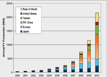
Figure 4.1.1.1.
World PV Cell/Module Production from 1990 to 2010
may be to run into a potential roadblock for PVs in the future if the commonly used materials are no longer available at economic prices.
The impact of nanotechnology has already been emphasised: it offers the possibility to harvest the full solar spectrum by quantum related phenomena such as Multiple Exciton Generation (MEG), the use of Intermediate Band (IB) materials, or the tailoring of the solar cell absorption through size tuning of nano-structures embedded in the active device area. Despite the fact that for some of the ideas it has been possible to show a proof of concept, their implementation within a large-scale, mature technology requires extensive sci-entific investigations and technological development.
Looking at the overall picture, it is important to note that silicon is still the dominating material with more than 85% of the total market for PV panels. This suggests that for the next 10–20 years significant research activities will be focussed on the use of silicon-based or silicon-compatible thin film structures. These materials include, of course, nanodots, nanowires, nano-tubes and other kinds of nanostructures able to improve the direct conversion of photons into electrical charges.
Moreover, while in the past most attention has been dedicated to the active part of solar cells (the region where photons are absorbed and create electronen–hole pairs), the new concepts of PV devices evidence the criti-cal role of all parts forming a solar cell: anti-reflecting coating, transparent conductive oxides (TCOs), metallic contacts, interfaces and substrates. Therefore, for exam-ple, the deposition of TCO is also a critical issue for the next generation solar cells.
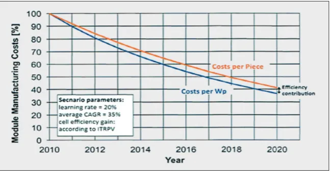
The PV industry has demonstrated its capability to lower the costs of PV systems in terms of cost per
Watt-peak (Wp) systematically over the last few decades following a learning curve with a learning experience in the order of 20%. This means that for every doubling of cumulative production, the cost decreases by 20%. However, it is of fundamental importance to realise that increased efficiencies contribute to cost reductions not only on module level – where most of the materials research is currently carried out – but also on the balance of system level.
Further large scale implementation of PV modules will also require intelligent modules in order to minimise losses attributed to partial shading or power fluctuations. To realise such intelligent modules, smarter control strategies and alternative power electronics topolo-gies that dynamically optimise the yearly electricity production of these modules have to be developed and integrated. There is also need to control parameters (such as the conversion factor of DC/DC converters) in real time. Additionally, monitoring devices (such as distributed temperature sensing) would enable the plant-level controller to optimise the energy yield – ultimately we might be able to make trade-offs between lifetime and maximising power here and now. Technology wise, this implies that additional power electronic circuits and sensors need to be placed in and around the module. Materials research is urgently needed to realise such components.
Future grid-connected PV systems will be subject to more stringent regulatory requirements for the deliv-ery of “ancillary services” to support the electricity grid when reserve and reactive power injection (for voltage support) has to be delivered. As the electricity grid has to deal with positive as well as negative balances, this involves the “shaving” of peak production and
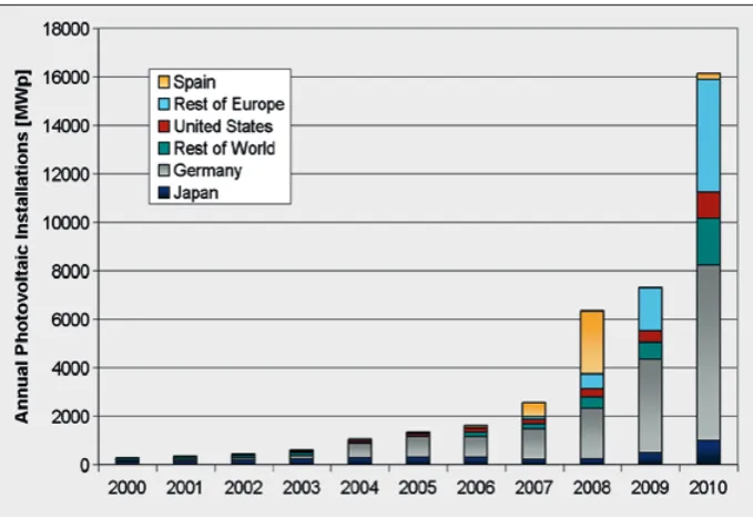
tempo-Figure 4.1.1.2
Annual Photovoltaic Installations from 2000 to 2010
rarily boosting power output. Lowering the output is easily achieved by moving away from the Maximum Power Point (MPP), but when storage is available, the energy conversion can be kept at maximum level and the output difference stored for later recovery.
Such a storage function may be centralised or distrib-uted – possibly a micro-storage for short term needs will be introduced at the module level in close conjunction to DC/DC converters. These storage components could consist of improved supercapacitors with low leakage and innovative thin-film battery approaches.
To realise such innovative approaches needs further development of the respective power components and storage technologies as solar modules increase in tem-perature during operation which is not favourable for the lifetime of current power electronics and storage technologies.
4.1.2 Biomass
Biomass is a renewable energy resource derived from waste. Biomass comes from both human and natu-ral activities and uses by-products from the timber industry, agricultural crops, raw material from forests, household wastes, and wood. Like wind, solar and other forms of renewable energy, biomass produces lower amounts of CO2 emission than its fossil fuel counter-parts. Therefore, the main driver for the deployment of biomass in Europe is the need to reduce carbon dioxide emissions and ensure a secure energy source.
Biomass can be converted into methane and various types of biofuels and used in numerous appli-cations. Synthetic natural gas is, for instance, already being used to produce biodiesel, bio-oil, and biofuel. The conversion of biomass to bioenergy involves materi-als and catalysts in many processes. For example, in the conversion of wood to methane, wood gasification may be performed in a fluidised bed with abrasion resistant and catalytically active materials, where the resulting
raw producer gas is cleaned from sulphur species by an absorber material and finally converted over a methana-tion catalyst.
Research has to be focused on the investigation and further development of the materials involved in bio-mass conversion with the following characteristics: • Materials that keep their high initial catalytic activity
even in highly contaminant-loaded hot gas streams • Materials that are not affected by the high
tempera-tures in these conversion processes
• Abrasion resistant materials when used as fluidised bed material
• Materials that are cheap and easily processable as well as being sufficiently resistant to corrosion. This could either be achieved by careful tests of known alloys or by new materials developed for this particular appli-cation. New coatings, which prevent the attack of corrosive inorganics at the underlying metal surface could also provide a solution
4.1.3 Thermo-Electric Energy
Thermoelectric generators enable the direct conversion of heat to electricity, but at present they are only used in a few niche applications such as supplying the energy for spacecraft and satellites, in Peltiercoolers in labora-tory instrumentation or for medical applications. The efficiency of thermoelectric devices depends on a figure of merit Z which increases with electrical conductivity and temperature and quadratically with the Seebeck coefficient but decreases with thermal conductivity. Previously thermoelectric materials in their bulk form were based mainly on compounds containing heavy elements like bismuth telluride or selenide, or lead compounds, but also on bulk SiGe alloys. To reduce thermal conductivity by enhancing phonon scattering, more advanced bulk materials were based on partially filled structures like skutterides (e.g. those based on alloys of CoSb3) /refs ADM, THB/ have pioneered the
Figure 4.1.1.3
Monocrystalline Si Solar cells
Source: First Solar Manufacturing GmbH, Frankfurt (Oder)
Figure 4.1.1.4
Thin-film solar module
use of quantum confinement phenomena in quantum wells, in quantum wires and quantum dots to enhance the Seebeck coefficient, a field which receives a lot of attention particularly in the US. The new advanced thermoelectric bulk materials contain nanoscale inclu-sions /ref ADM/ with typical dimeninclu-sions of the order of 10 nm, for an efficient reduction of the thermal con-ductivity, without affecting the electrical conductivity too much, and an increase of the Seebeck coefficient. In particular the production of cost-effective nanocompos-ites with randomly distributed nanoparticles has turned out to be essential for future wider-spread use. Whereas the commercial market for thermoelectric devices so far is rather small at present this could grow with improved materials.
Apart from various semiconducting alloys and compounds with metallic or semimetallic inclusions, metal oxides have been identified as promising ther-moelectric materials. They are chemically stable even at very high temperatures of ~1200 K. Research in this field has already produced most encouraging results.
4.1.4 Nuclear Energy
Nuclear power currently accounts for about 20% of worldwide electricity production and the demand is steadily increasing. As a consequence the demand per production unit increases and the enhanced yields result in the fact that materials used as structural components or as fuel must operate under extreme conditions. In addition, the waste stockpile increases and ecological solutions are required.
Throughout the last 20 years, Europe has been a leader in nuclear materials science in strong coopera-tion with American, Asian and other countries. The studied materials are component materials for future generation units such as advanced fission/fusion sys-tems, and structural materials for thermal reactor units.
Fuel materials including the fuel matrix and targets for transmutation have to be considered taking into account their operation as well as the waste materials for disposal.
A common topic for future nuclear power systems is the trend towards high operation temperatures and high burn-up. An additional key challenge for the suc-cessful development of materials for fission and fusion systems is the harsh neutron irradiation environment.
A combination of multiscale modelling and
advanced experimental test techniques need to be used investigate and to resolve issues related to the different types of materials used:
• Component materials for advanced fission/fusion systems
• Component materials for thermal reactor units • Fuel materials, fuel matrix and targets for
transmutation
• Waste form materials for disposal
Research of new materials including metals, car-bides, nitrides, oxides utilised as alloys, solid solutions or composites should focus on higher stability or better mechanical performance.
Characterisation of these materials is carried out using advanced techniques; ex-situ studies on irradiated material and at elevated temperatures are required and are performed with accelerators and in piles in reac-tors. Characterisation should be performed in-situ by non-invasive techniques (by for example using inert windows for observation and analysis via video, Raman, DRS, XAFS, PIXE, etc).
The final goal is to develop advanced materials as component for fusion and generation IV (GENIV) fis-sion systems; highly reliable materials for structural parts of thermal reactors with excellent behaviour in-pile; economical fuel materials and targets for trans-mutation; and ecological waste form materials for
Figure 4.1.1.5
Module manufacturing costs based on an empirical learning curve with a learning rate of 20 %
geological disposal. R&D efforts should therefore be directed into making the use of nuclear materials more sustainable, safe, economical and ecological.
4.2 Energy Storage and Distribution
Several of the energy sources mentioned above are not available constantly and in a predictable manner, and hydro- and nuclear power plants cannot react quickly enough to short-term fluctuations in energy demand. Therefore energy storage is a key requirement and in this context three major technological solutions are considered.
In the first place, batteries might play a role pro-vided that high-capacity batteries are available. These are needed for electric vehicles, and can be used for decentralised storage. The challenge is to achieve the required capacities within the time-frame defined by industrial needs. Anyhow, battery development will be very important for local energy storage at a smaller scale. Similarly super capacitors will mainly be used for fast energy storage/delivery at a small scale.
A very promising technology, but so far not fully developed, is energy storage in the chemical form, using electrical energy to produce methane, ethanol, or other synthetic fuels essentially from CO2 and H2O. The fuels produced in this way have a very high energy density, are easy to store and transport, and can easily be con-verted back to electricity or other energy forms using conventional as well as novel techniques. This technol-ogy can also contribute to a reduction of CO2 emissions from conventional caloric power plants.
A key issue in the distribution of energy is the development of better grids (“smart grids”).
4.2.1 Li-Ion Batteries
The challenges for Li-ion battery systems are very high, due to the rapidly increasing requirements for high performance energy storage systems. Studies sug-gest an increase of the market volume for batteries based on Li-ion technology of 77 B € in 2025. In gen-eral batteries store chemical energy and, on demand, convert it directly into electrical energy to power a variety of transportable applications such as cellular phones, laptops or other portable electric devices. These applications require compact, lightweight, and low cost storage systems. Requirements for materials used for energy storage systems in electric vehicles are deliverance of high currents for fast charging/dis-charging, high energy density, long cycle life, safety and low cost.
Current rechargeable lithium ion cells suffer from safety problems, low energy density, complicated battery designs, toxicity issues (cobalt), and limited resources of raw materials.
The development of next-generation lithium bat-teries requires the investigation of high-performance materials and the exploitation of new systems. The most promising research directions are:
• In the near futurenovel carbon varieties includ-ing nanostructures, lithium alloys, and improved silicon structures are promising candidates for the anode. For cathodes, high voltage materials (~ 5V) such as Ni-Mn-Co oxides show high promise and are a “hot” research topic. With improvement in the performance of new electrode materials, the demands on the electrolyte are also increasing These might be met by polymer electrolytes and ionic liquids. Beyond the chemical issues, nanoscaling and -structuring will play an important role in the future of batteries technology.
• In the longer term, the design and development of systems such as Li-sulphur and Li-oxygen (air) batter-ies should be envisaged. It expected that these systems can exceed the energy density of “conventional” Li-ion batteries by roughly tenfold.
• Other systems, e.g. Zn-air or organic batteries are promising and have to be considered on the long term, despite the fact that at the moment the replacement of the Li-ion technology by other cell chemistries is not yet foreseen.
Other future research directions are the development and fabrication of thin film Li-ion batteries which can be used to power added functionalities in devices such as credit cards.
4.2.2 Supercapacitors
In recent years supercapacitors (SCs) have found their market niche for several applications and the corre-sponding world market is expected to increase to US$ 900 M for large devices (> 300 Farad) by 2015. If small capacitors (those found in cameras, mobile phones) are included, the market is estimated to be well above US$ 2 B.
Supercapacitors have proven long cycle life (> 500 000 full Depth of Discharge (DOD) cycles) with high efficiency and high power. However, in many applications the relatively low energy of SCs is a major issue.
• Novel electrode and electrolyte materials which allow for an increased cell voltage
• Hybrid designs by utilising battery and capacitor materials
4.3 Carbon Dioxide as a Raw Material and a Future Chemical Fuel for a Sustainable Energy Industry
4.3.1 General Objectives
The continuous increase of the concentration of CO2 in the atmosphere, and the related consequences, have pushed the European Parliament and the European Commission to launch a programme for CO2 seques-tration in the ground (more details can be found in many reports, including STOA (IP/A/STOA/FWC-2005-28/SC20 and 2008-01; PE 416.243). According to the European SET plan, by 2020 20% of European emission should be captured and stored. It has to be noted that the world total emission of CO2 will reach 30 gigatons in 2010.
In order to achieve the plan’s objectives, industrial units are planned, with a unit price of approx €1.2 bn for an adsorption capacity of 5 millions tonnes per year. In the future, several hundred will be needed to make a significant impact. The three foreseen essential steps are: collect the CO2 as close as possible to the source, transfer it by pipeline to adequate locations and pump it in the soil.
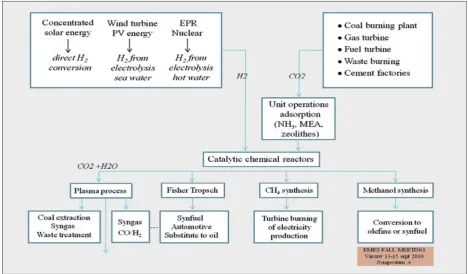
We propose to consider CO2 as a raw material which can be recycled as a chemical fuel, which can be used as an energy source, thus generating a completely new industry in Europe.
4.3.2 How does this Process work?
In the first step CO2 has to be collected. Work is starting at an industrial scale to establish the efficiency, the cost and the risks of these processes using amine, ammonia or zeolites for the adsorption step. The raw material CO2 (as gas or liquid) has to be chemically reduced by hydrogen to make a synthetic fuel (synfuel).
Industrial pilot plants for carbon dioxide capture for thermal power stations, at smaller capacity between 10 to 200 MW, are working today (BASF, TOTAL, ALSTOM, Dow Chemical, IFP, RWE, BP, Power Pass Corp, etc.).
The details of the different reactions have already been considered in two workshops (2008/Paris and 2009/Strasbourg) and a symposium at the E-MRS Fall Meeting in Warsaw in September 2010. During
the Energy Conference organised in Fall 2009 in Stockholm under the Swedish Presidency, Prof. George Olah, Nobel Laureate in Chemistry confirmed our model (see Figure 4.3.2.1 below from his presentation). The efficiency of the whole process, i.e. the economics, will depend largely on the quality of the catalysts and progress using nano-catalysts have been shown very recently, as well as the splitting of H2O by solar photons.
These technical proposals have received strong sup-port from J.E. Stiglitz (Nobel Prize in Economy 2001) who declared recently “should the world endeavour to have carbon emissions paid at their real price… (it is essen-tial) to promote incentives for innovations and investment in all techniques, companies, (and) home equipments which are more energy efficient”.
4.3.3 Applications
As a large spectrum of applications of chemical fuels is possible, we restrict ourselves here to the chemical storage of excess electricity.
European authorities have decided that by 2020 a larger fraction of our electricity should be gener-ated by renewable energies, photovoltaic, wind, and ocean. (Project 20-20-20). However, these are non-constant sources of energy over time and it will become more and more difficult to stabilise the grid (e.g. the incident in Germany during 2009). Storage of
elec-Figure 4.3.2.1. Technological Carbon Cycle
tricity is therefore a necessity; however, this is not possible directly: batteries will be insufficient as will be pumped-storage hydro-electric installations.
Large power plants, especially nuclear reactors, are not very flexible as a result of which the electricity price in Europe changes in the same day from about 5 cents to more than 1.0 € per kW/h. Low cost electricity can be used to dissociate the water molecule H2O and to generate the hydrogen H2 needed for CO2 reduction (it would even be possible to combine photovoltaic and nuclear in a same plant, one part of the electricity com-ing in the daytime from PV and from the large plant overnight). This chemical transformation of CO2 into methane (CH4) or methanol (CH3OH) or synfuel will establish the capability to store electricity through a chemical process.
Even if not considered here in detail, it is obvious that these chemical fuels can become the energy carrier for transportation. The thermal engines in cars cannot be replaced in the short term at large scale either by fuel cells, or by batteries, because both the technologi-cal and economitechnologi-cal developments are not mature for large energy storage. But an evolution of the engines will make possible the use of the fuels generated by CO2 recycling as proposed in Figure 4.3.3.1.
4.3.4 Key Steps for a Development based on CO2 Valorisation
• The development of e H2 production: efficiency from electrolysis of sea water is one of the most ambitious goals and is dependent on catalysis research for new electrodes. Today, hydrogen is mainly produced from methane derived from fossil fuels large oil fields or shale gas.
• Secondly, catalytic materials are the key step: for the redox recycling of CO2, strong scientific research network is needed for high efficiency stable catalytic materials in order to develop exothermic catalytic reactors with high efficiency conversion rate.
For large chemical plants the cost of the catalyst is one of the main factors that contribute to the cost of the process. Therefore, this key step needs to be developed by taking into account the efficiency and the selectivity of the catalyst including the support, the new kinds of spinels or perowskites which are able to replace expen-sive metals such Pt, Rh, Pa or rare earths such as Pr, Nd, Pm. Nanostructures may also become of great importance.
• Develop economical and technical research on the engineering of the grid control in a mixed flux of con-ventional and renewable energy supply. At the same time, new fields of scientific research can be explored. One of these is the direct splitting of H2O by solar pho-tons. It should however be noted that already today
there are overseas laboratory scale instruments, and large scale facilities are under construction.
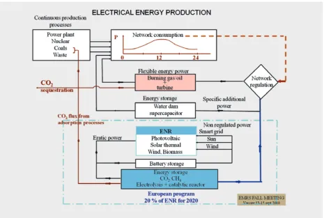
• Carbon dioxide as a raw material for electrical network regulation
Taking into account this proposal, we can imagine a strong connection between the traditional electri-cal network and its regulation/control by including a large amount of renewable energy systems such as photovoltaic panels, wind turbine, biomass combus-tion, or thermal solar turbine. We have to remember that the goal is to reach 20% to 30% renewable capac-ity in the next ten years.
The flow sheet below provides an overview (Figure 4.3.4.1).
4.3.5 World Wide Equipment under Construction
From the most recent publications, one can observe the starting up of industrial and some pilot plants. Energy storage from the chemical reactions of carbon dioxide and hydrogen allow transformation from a gas phase to a liquid phase.
From the publications we can highlight the pilot plant developed by Professor K. Hashimoto to propose
energy storage from photovoltaic panels via carbon dioxide reduction by hydrogen produced by an elec-trolysis plant. The key steps are elecelec-trolysis and CO2 reduction.
4.3.6 Safety and Sustainability of the Process
The chemicals and materials involved in the whole pro-cess are CO2, H2O, H2, CH4 and CH3OH, all chemicals which are largely in use today. Of the metallic cata-lysts, those with nano-structures have to be handled like other metallic nanoparticles, as used in cosmetics or even medicine (MRI).
The large development of new catalysts is one of the key aspects of these processes. Most of the catalysts are formed from amorphous Ni-Zr and Ni-Zr-rare earth element alloys. Ni/(Zr-Sm)Ox catalysts are the main powder used for mass production but in order to avoid dependence on rare earths, new catalysts using Ni sup-ported by tetragonal ZrO2 and others using Ni-Zr-Ca or Ni-Zr-Mg supported on tetragonal ZrO2 stabilised by Ca2+ or Mg2+ have been developed. These new nano-structured materials with large surface area and strong stability to the carbon dioxide impurities permit an increase in efficiency of the process and a decrease in cost.