National Conference on Advances in Engineering and Applied Science (NCAEAS) 29th January 2018
Organized by : Anjuman College of Engineering and Technology (ACET) Nagpur, Maharashtra, India, In association with
International Journal of Scientific Research in Science and Technology
Design and Analysis of SRAM and DRAM using Microwind
Software
Abhilesh Kedar, Aditya Verma, Latika Raut,Pinki Kumbhare, Rajashree Karoo, Rajeshree Zade, Prof. Omprakash K. Piprewar
Department of Electronics and Telecommunication Engineering S. B. Jain Institute of Technology, Management and Research, Nagpur, Maharashtra, India
ABSTRACT
This study analyses an minimizing the power consumption during write and stand by operation and propagation delay during write in 6T SRAM cell and 1T1C DRAM cell. And these cells are designed using Microwind3.5 Software in 45 nm and 32 nm CMOS Technology. The 6T architecture of SRAM cell is implemented using 32 nm CMOS Technology and Result have been compare with that of 45 nm CMOS Technology. Also the 1T1C architecture of DRAM cell is implemented using 32 nm CMOS Technology and Result have been compare with that of 45 nm CMOS Technology. The result of the delay and power dissipation of SRAM and DRAM with the applied power supply is presented. The graph of Voltage vs Time is plotted using Microwind3.5 software.
Keywords: SRAM, DRAM, MICROWIND, CMOS Technology
I.
INTRODUCTION
In the design of many modern electronic digital design semiconductor memories plays an essential role where there is need for data storage, such as computers based application and microprocessors found in many application fields of image processing, satellite signal processing, and even consumer electronic devices. In this era CMOS technology scaling will be a main drive force of the electronics industry and also for faster and denser integration it provided a path.
As the length of channel is reduced, the performance of the transistor improves, the density improves and the power per switching event
decreases. Over the last two decades, the number of components per chip and the system performance is improving exponentially. Major factors influencing the need of low power design are increasing different personal computing devices viz. wireless communicating devices; smart cards, PDA’s, digital pens and audio and video based multimedia products etc.
designs with the aim of degrading the power consumption during read write operations of SRAM.
DRAMs is categorized as volatile memory which means it loses their memory content when the power to the host system is turned off; but unlike DRAM, SRAM is non destructive read-out (NDRO). SRAMs consume very much less energy than DRAMs and thus is an automatic choice over the latter. SRAM doesn't require a refresh cycle because Data don't "Leak Away".
All the simulations are done with the help of Digital Schematic (DSCH) editor and the Microwind3.5 software. Microwind is a tool for designing and simulating circuits at layout level. The tool features full editing facilities (copy, cut, past, duplicate, move), various views (MOS characteristics, 2D cross section, 3D process viewer), and an analog simulator. DSCH is a software for logic design. Based on primitives, a hierarchical circuit can be built and simulated. It also includes delay and power consumption evaluation. Schematic design simulations are performed and the functionality verifications is done with the help of DSCH software. The Verilog code is generated for these modules and is being called from Microwind software to generate a layout. A functional verification is also done with the layout output of each module. Layout diagrams, power analysis results are obtained in the result section.
II.
PROPOSED DESIGN
1. 6T SRAM Cell
A SRAM is a bi-stable element used to data as voltage potential. The basic 6T SRAM cell consist of cross coupled CMOS inverters. The inverter usually have a large nMOS width as compared to the pMOS
width. This often causes switch threshold of inverter to be close to nMOS threshold voltages.
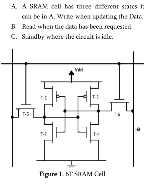
A. A SRAM cell has three different states it can be in A. Write when updating the Data. B. Read when the data has been requested. C. Standby where the circuit is idle.
Figure 1. 6T SRAM Cell
A. WRITE OPERATION
Write operation starts with assigning the values to be written at the Bit and its complimentary value at Bit'. In order to write '1' Bit is pre-charged with high voltage and the complimentary value '0' is assigned to Bit'. When T-5 and T-6 are set in ON condition by asserting WL 'high', the values assigned at Bit get stored in the latch as Data. The T-5 and T-6 MoSTs are designed to be much stronger than the relatively weak transistors in the cell, T-1, T-2, T-3 and T-4 so that they are able to override the previous state of the cross-coupled inverters.
B. READ OPERATION
transistors T-5 and T-6 after pre-charging both the Bit and Bit' lines to a logical 1. The second step occurs when the values stored in Data and Data' are transferred to the Bit lines by leaving Bit at its pre-charged value and discharging Bit' through T-4 and T- 6 to a logical O.
C. STANDBY STATE
For the idle state, the word line (WL) is not asserted and the access MoSTs T-5 and T-6 disconnect the cross coupled inverters from the bit lines. The two cross coupled inverters INVI and INV2 formed by T-l, T-3 and T-2, T-4 they are not connected from any external circuits.
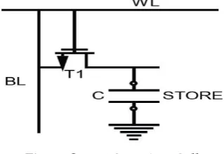
2. 1T1C DRAM Cell
A DRAM is the main memory used for all desktop and larger computers. DRAM cell is made up of a single MOS transistor and a storage capacitor. Each storage cell contains one bit of information. This charge, however, leaks off the capacitor due to the sub-threshold current of the cell transistor. Therefore, the charge must be refreshed several times each second.
Figure 2. 1T1C DRAM Cell
The write operation can be done by placing a “1” or “0” charge into the capacitor cell. This is done by opening the cell transistor (gate to Vdd) and presenting either Vdd or ground at the capacitor. The word line is then held at ground to isolate the capacitor charge. This capacitor will be accessed for either a new write, a read, or a refresh.
III.
IMPLEMENTATION USING MICROWIND
MICROWIND is integrated EDA software encompassing IC designs from concept to completion, enables chip designers to design beyond their imagination. MICROWIND integrates traditionally separated back-end and front-end chip design into an integrated flow, accelerating the design cycle and reduced design complexities.
The 45 nm technology invented in 2007 & it has effective Gate length of 30 nm whereas The 32 nm technology invented in 2009 & it has effective Gate length of 25 nm. Compared to 45 nm technology, the 32 nm technology offers 30% increase in switching performance, 30% less power consumption, double higher density, two time reduction of the leakage between source and drain and through the gate oxide. At each lithography scaling, the linear dimensions are approximately reduced by a factor of 0.7, and the areas are reduced by factor of 2. Smaller cell sizes lead to higher integration density which has risen to nearly 1.5 million & 2.8 million gates per mm2 in 45 nm & 32 nm technology respectively.
IV.
SIMULATION RESULT
1. 6T SRAM Cell
Figure 3. 6T SRAM Cell using DSCH editor
In figure 3 it is shown that SRAM cell uses two inputs lines namely WL (write line) and BL (bit line). Write line acts like an enable pin which is connected to gates of the transistors T-5 and T-6. BL represents the bit that needs to be stored and BLB its complement. To perform write operation, we need to keep the BL in the required state by keeping the WL pin in low state and then change the state of WL pin to high. The two inverter circuits connected to each other are responsible for holding the data. To perform read operation, we need to make BL and BLB high. After this, either of the BL and BLB lines will be pulled low because it gets discharged due to the zero state present on one of the inverters. Figure 4 shows the timing diagram for function verification.
Figure 4. Timing diagram of 6T SRAM Cell
The layout of 6T SRAM Cell using Microwind3.5 is shown in figure 5.
Figure 5. Layout of 6T SRAM Cell
2. 1T1C DRAM Cell
The circuit diagram for 1T1C DRAM Cell is shown in figure 6 which is implemented by using DSCH editor.
In figure 6 it is shown that DRAM cell uses two inputs lines namely WL (write line) and BL (bit line).In DRAM also write line acts like an enable pin which is connected to gate of the transistor. BL represents the bit that needs to be stored. To perform write operation, we need to keep the BL in the required state by keeping the WL pin in low state and then change the state of WL pin to high. The nMOS transistor acts like flip-flop to store the data. To perform read operation, we need to make BL high. Figure 7 shows the timing diagram for function verification.
Figure 7. Timing diagram of 1T1C DRAM Cell
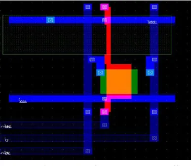
The layout of 1T1C DRAM Cell using Microwind3.5 is shown in figure 8.
Figure 8. Layout of 1T1C DRAM Cell Table 1. Comparitive Analysis Of Sram And Dram
Contents
Sr. no.
Parameters SRAM
DRA M
Pre- 0.12ns 0.15ns
charged
1 Delay Read 0.24ns 0.4ns Write 0.30ns 0.37ns
2 Power Consumption
0.185m
W 0.20mW
3 Area Required
2375um ^2
3580um^ 2
V.
CONCLUSION
From this Paper After doing Design and Analysis we have found the comparative Evaluation between different parameters of SRAM and DRAM cell at 45 nm and 32 nm it has shown that the SRAM cell has better performance as compare to DRAM cell. To have better result our future work will concern with 22-nm Technology.
VI.
REFERENCES
[1].Peter Bukelani Musiiwa and Shyam Akashe ," Comparative Evaluation of different 3T DRAM Cells at 45nm Technology" International Conference on Communication Networks (lCCN), 2015
[2].Saraju P. Mohanty, "CSCI 5330 Digital CMOS VLSI Design", University of North Texas. [3].P. Upadhyay, R. Mehra and N. Thakur "Low
Power Design of an SRAM Cell for Portable Devices" Int'l Conf. on Computer & Communication Technology IICCCI' 101 pp. 255-259.
[4].Saurabh and P. Shrivastav, "Low Power 6T-SRAM", IEEE 2012, 978-1-4673-3136.
[6].Acida V.V., Mohamed Salih K.K., "Design Of Low Power High Density SRAM Bit Cell", International Research Journal of Engineering and Technology, Vol.4, Issue 4, June 2017 e-ISSN: 2395 -0056, p-e-ISSN: 2395-0072
[7].Prateek Asthana, Sangeeta Mangesh, "PERFORMANCE COMPARISON OF 4T, 3T AND 3T1D DRAM CELL DESIGN ON 32 NM TECHNOLOGY", 2014 pp. 121–133, 2014. [8].Chakka Sri Harsha Kaushik, Rajiv Reddy