CMOS INTEGRATED HALL ELEMENTS PARAMETERS SIMULATION
AND REAL STRUCTURES BEHAVIORS MEASURING
Yury Goryachkin1, Alexander Odnolko2, Mikhail Pavlyuk2, Alexander Svistunov2 and Danil Demidov2
1National Research Mordovia State University, Saransk, Mordovia, Russian Federation 2JSC «ICC Milandr», Zelenograd, Moscow, Russian Federation
E-Mail: [email protected]
ABSTRACT
The article describes research results and comparative analysis of different configuration of Hall elements designed within the XFAB XH035 process. Three most common Hall elements structures: Rectangles, cross diamond-shape and quadruple Hall element, consisting of four paralleled single Hall elements of rectangular configuration, researched. The relationship between drain current, offset voltage, sensitivity and drain voltage and relationship between drain current, sensitivity and dimension impact of Hall element (width and length) researched. Analysis carried out to choose the most efficient configuration of Hall element in conjunction with following characteristics: current consumption, sensitivity and offset voltage to use the Hall element as a part of integrated circuit with linear output. In addition, the comparative analysis of main characteristics of designed Hall elements and Hall elements manufactured by bipolar technology, by “Silicon on insulator” technology and by gallium-arsenide technology, carried out.
Keywords: hall element, CMOS-technology, hall voltage, drain current, sensitivity, offset voltage, simulation.
1. INTRODUCTION
A few XFABCMOS processes analyzed as production technology to create the linear integrated Hall element composed of IC’s in [1]. Such IC’s contain Hall element, where Hall voltage changes proportionally to magnetic field induction. As a rule, these IC’s contain sensor’s signal amplifier. In case when there is no external magnetic field the IC’s output voltage, taken for reference level, is equal to half supply voltage. When positive magnetic field is registered, output voltage is higher than reference level, otherwise when magnetic field is negative output voltage is lower, although it remains positive value [2].
Hall element for such IC designed in n-Well and pinched from above by p-type layer. Thus, n-type controlled channel included between p-n junctions formed. By the fact, such structure is a FET. The structure of such Hall element described in [1, 3]. IC’s and Hall element supply voltage is 5 V.
The main criterion to choice the technology was obtaining of maximum Hall voltage. The following requirements have to be satisfied: low doping concentration in active layer to achieve maximum mobility and high thickness of active layer to prevent channel overlap. Four X-FAB processes meet the requirements: XT018, XC06, XT06 and XH035. By using TCAD simulation it was founded that to create integrated linear Hall element as a part of IC the most appropriate Hall element characteristics (sensitivity, current consumption and operating range) provides XH035 process.
2. RESEARCH TASKING
Hall elements of three most common types
and width), S - source, D - drain, G - gate, HL and HR - left and right Hall contacts respectively.
Second diamond shape structure (Figure-1, d) is included to show, how L length decreasing influence on the configuration of source and drain contacts
. a) b)
c) d) Figure-1. Hall elements’ structure - rectangle (a), cross (b), and diamond shape (c and d) pWell layer purpose was
Cross with pWell
190 80 0,42
190 100 0,53
190 120 0,64
95 60 0,64
Cross without pWell 190 100 0,53
Diamond shape with pWell
265 265 1
180 265 1,5
95 265 2,8
132 132 1
Diamond shape without pWell 265 265 1
The following dependences verified:
Drain current (ID) vs drain voltage(VD) dependence;
Offset voltage (V0) vs drain voltage (VD)dependence;
Sensitivity (S) vs drain voltage (VD)dependence;
Drain current (ID) and sensitivity (S) vs dimensions (W - width and L - length) dependence;
Research results and comparative analysis of these Hall elements’ configurations is bellow.
3. DRAIN CURRENT VS DRAIN VOLTAGE DEPENDENCE
Drain current vs drain voltage dependence is volt-ampere characteristic (VAC).
VAC measuring conditions. Source, drain and substrate connected to common bus potential. VD changed in range from 0 to 12 V by step 1 V and ID current measured. VAC diagrams created after all measurements.
Figures 2, 3 and 4 shows different configuration Hall elements VACs with pWell and without pWell.
a) L = 210 µm, W = 274 µm with
a) L = 190 µm, W = 100 µm with
pWell b) L = 190 µm, pWell W = 100 µm without Figure-3. Hall elements’ VAC of cross configuration.
a) L = 265 µm, W = 265 µm with
pWell b) L = 180 µm, pWell W = 265 µm with
c) L = 95 µm, W = 265 µm with
pWell d) L = 265 µm, pWell W = 265 µm without Figure-4. Hall elements’ VAC of diamond-shaped configuration.
As can be seen on diagrams, Hall elements’ VAC with pWell layer is a typical FET with p-n junction VAC with, Hall elements’ VAC without pWell layer is a typical resistive dependence. For all Hall elements with pWell layer VAC extreme begins from voltage 6-7 V, VAC saturation begins from voltage 9-10 V. For Hall elements
So, if Hall sensor IC power supply VDD= 5 V, Hall elements with pWell is preferable in comparison to Hall elements without pWell.)
silicon has strong piezoresistive effect and Hall element being four-pole reacts on offset voltage. This reaction appears through mentioned effect.
Layers’ layout combination imprecision relative to each other brings a substantial contribution to integral
offset voltage vs source voltage for different configuration Hall elements measured. V0 offset voltage is a voltage
difference between Hall contacts HL and HR with magnetic field absence.
a) L = 210 µm, W = 274 µm with
pWell b) L = 210 µm, pWell W = 274 µm without Figure-5. Offset voltage on drain voltage dependence of rectangular
Hall elements. (1, 2, 3 and 4 - samples’ numbers).
Figures 5, 6 and 7 shows typical dependences for 4 Hall elements samples of different configurations with and without pWell layer.
a) L = 190 µm, W = 100 µm with
pWell b)
L = 190 µm, W = 100 µm without pWell
a) L = 265 µm, W = 265 µm with
pWell b) L = 180 µm, pWellW = 265 µm without
c) L = 95 µm, W = 265 µm with
pWell d) L = 265 µm, pWell W = 265 µm without Figure-7. Offset voltage on drain voltage dependence of diamond-shaped
Hall elements configuration. (1, 2, 3 and 4 - samples’ numbers).
As can be seen from the diagrams, for Hall elements with pWell, offset voltage on drain voltage dependence manifold nature observed.
For example, in rectangular Hall elements for samples 1, 2 and 3 offset voltage rises linearly with voltage growing on drain to approximately 8-9 V, further saturation comes. For sample 4 there is dependence: offset voltage does not almost change when drain voltage increases to 5 V, with voltage rise to 9 V offset voltage rises sharply and then saturation comes.
In cross Hall elements for samples 1, 2 and 3 offset voltages on drain voltage dependence are like rectangular Hall elements dependences. Only for sample 4 Hall voltage does not almost depend on drain voltage and is no more than 0,3V.
A similar dependence nature of these two Hall elements configurations is associated with the fact that rectangular configuration is a particular case of cross configuration, i.e. differs from cross configuration only with Hall contacts smaller size (see Figure-1, a and b).
For diamond-shaped Hall elements, as can be seen from Figure-7, dependence manifold of offset voltage vs drain voltage observed, moreover for Hall elements with one L value and for different length values.
5. SENSITIVITY ON DRAIN VOLTAGE DEPENDENCE
Hall element’s sensitivity is a ration of Hall voltage to magnetic induction value and expressed in mV/mT. To define sensitivity dependence vs drain voltage one is to register Hall voltage dependence vs drain voltage at definite magnetic field induction value and then calculate sensitivity in mV/mT considering that Hall voltage rises directly-proportionally to magnetic field induction.
1 - Rectangular with pWell - L = 210 µm, W = 274 µm; 2 - Rectangular without pWell - L = 210 µm, W = 274 µm; 3 - Cross with pWell - L = 190 µm, W = 100 µm; 4 - Cross without pWell - L = 190 µm, W = 100 µm; 5 -Diamond-shape 1 with pWell - L = 265 µm, W = 265 µm; 6 - Diamond-shape 2 with pWell - L = 180 µm, W = 265 µm; 7 - Diamond-shape 3 with pWell - L = 95 µm, W = 265 µm; 8 - Diamond-shape without pWell - L = 265 µm, W = 265 µm.
Figure-8. Sensitivity dependence on drain voltage of different configuration Hall elements.
DIMENSIONS’ DEPENDENCEs
Rectangular shaped Hall elements simulation in TCAD carried in [1, 3]. It discovered that technology XH035 can provide the most optimal Hall elements’ characteristics (sensitivity, current consumption and operating voltages range) as a part of Hall element within IC. The simulated Hall elements’ structure and used models and physical effects were also described in [1, 3]. More detailed description of these models is in [11].
Further research results of different configuration Hall elements’ with pWell layer drain current and sensitivity on dimensions’ (length L and width W) dependences and comparison with simulation results will be described.
Measurements carried out at drain voltage VD= 5 V. Dependence diagrams of drain current sensitivity on W/L ratio for different Hall elements’ configurations constructed, based on measurements and calculation results. Figures 9, 10 and 11 shows the diagrams in comparison to modeling results.
Figure-10. Drain current and sensitivity dependence vs W/L ratio of cross Hall elements with pWell.
Figure-11. Drain current and sensitivity dependence vs W/L ratio of diamond-shape Hall elements with pWell.
As can seen from the diagrams, the most optimal characteristics combination of drain current and sensitivity has rectangular Hall elements’ configuration.
Diamond-shape has sensitivity comparable to rectangular hall element at W/L > 2, but drain current is higher. Cross configuration has not only the least drain current, but also minimal sensitivity. It Is corresponded with the fact that for cross W/L ratio is always less than 1, and besides Hall contacts’ sizes HL and HR are the same as D drain and S source contacts (see Figure-1, b). As it was shown in [1] to obtain maximum Hall voltage, Hall contacts have to be minimal dimensions (up to 10 µm) and W/L ration in the limits of 1.25 < W/L < 1.5.
Sensitivity on W/L ratio dependences diagrams show that the dependence nature for rectangle and diamond-shape differs from cross dependences nature. For rectangle and diamond-shape sensitivity with W/L ratio increase rises and at definite W/L value saturation comes. There is a extreme point for the cross, after which sensitivity decreases with W/L ratio growth.
In addition, diagrams show that simulation and measurements results have a good correspondence. For drain current simulation, maximum error does not exceed 9 %; maximum error on sensitivity simulation does not exceed 8 %.
7. COMPARATIVE ANALYSIS OF CHARACTERISTICS OF DESIGNED HALL ELEMENTS WITH DIFFERENT CONFIGURATION
Table-2 summarizes drain current (ID) measurement results, sensitivity (S) calculation and Hall elements of different configurations with and without pWell layer values of measured offset voltages |V0max| at drain voltage VD = 5 V.
Table-2. Test Hall elements of different configuration characteristics.
Configuration L, µm W, µm W/L ID, mA S,
mV/mT |V0max|, mV
Rectangle withpWell
210 210 1 0,66 0,405 7,8
210 242 1,15 0,76 0,438 5,2
210 274 1,3 0,86 0,45 7,7
105 137 1,3 0,86 0,45 8,4
Rectangle without
pWell 210 274 1,3 2,22 0,44 7,1
Cross with pWell
190 80 0,42 0,3 0,24 5,3
190 100 0,53 0,4 0,27 6,1
190 120 0,64 0,5 0,255 5,2
95 60 0,64 0,5 0,26 5,4
Cross without
pWell 190 100 0,53 1,1 0,28 6,8
265 265 1 0,15 0,12 0,14
Maximum offset voltage values observed for rectangular Hall elements (more than 8 mV). Cross Hall elements offset voltage value is less, but big enough (up to 7 mV). For diamond-shaped Hall elements maximum offset voltage values are much less and strongly depend on W/L ratio. If W/L = 1, maximum offset voltage values are less than 0, 15 mV. If W/L = 1, 5 maximum offset voltage values are almost 1mV. If W/L = 2, 8 maximum offset voltage values are almost 3 mV.
As well, the table shows that for rectangle and cross pWell layer absence does not almost influence on offset voltage at the same W/L ratio values. But for the diamond pWell layer absence leads to sufficient (3-4 times) offset voltage increase at the same W/L ratio values. Therefore, as one can see from the Table-2, the most optimal characteristics combination of drain current and sensitivity has a rectangular Hall element configuration (at W/L = 1,3 ID = 0,86 mA, S = 0,45 mV/mT). Diamond-shapes Hall element are higher drain current and lower sensitivity (at W/L = 2, 8 ID = 1, 43 mА, S = 0, 41 mV/mT). However, as it mentioned above, rectangular Hall element has much higher offset voltages in comparison to diamond-shaped Hall element.
As it known [10], to compensate offset voltage one can use several Hall elements, parallel connected and turned relative to each other at 90° angle (so called “orthogonal shift”). Two Hall elements (doubled) or for Hall elements (quadruple) connected in such a manner. Doubled Hall element in comparison to single allows reducing offset voltage by several times, and quadruples by a lot.
In this regard, at test dies quadruple Hall elements were manufactured, containing 4 Hall elements
L = 210 µm, W = 274 µm with pWell Figure-12. Offset voltage vs drain voltage dependence
of quadruple rectangular Hall elements. (1, 2, 3 and 4- samples’ numbers).
As one can see from the Figure-12, offset voltage for quadruple rectangular Hall element is many times less than offset voltage of s single rectangular Hall element (see Figure-5, a). In particular, at a drain voltage VD = 5 V, quadruple Hall element's offset voltage does not exceed 1 mV, for a single Hall element offset voltage comes to 7 mV.
9. HALL ELEMENTS COMPARISON TO ANOTHER HALL ELEMENT
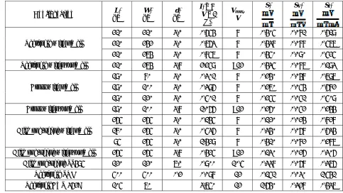
Table-3. Hall elements’ characteristic.
Configuration µm L, µm W, µm d, (IV, mA = 5
V)
Vmax,
V
S, SV, SI,
Rectangle with pWell
210 210 3,0 0,654 8 0,405 0,081 0,619 210 242 3,0 0,763 8 0,438 0,088 0,577 210 274 3,0 0,857 8 0,450 0,090 0,525 Rectangle without pWell 210 274 3,8 2,259 >12 0,435 0,087 0,193
Cross with pWell
190 80 3,0 0,301 8 0,240 0,048 0,797 190 100 3,0 0,396 8 0,270 0,054 0,682 190 120 3,0 0,501 8 0,255 0,051 0,509 Cross without pWell 190 100 3,8 1,066 >12 0,260 0,052 0,244
Diamond-shape with pWell
265 265 3,0 0,145 8 0,120 0,024 0,828 180 265 3,0 0,536 8 0,340 0,068 0,634 95 265 3,0 1,429 8 0,410 0,082 0,287 Diamond-shape without pWell 265 265 3,8 0,425 >12 0,130 0,026 0,306 Diamond-shape SS495 120 120 7,0 0,900 10,5 0,338 0,068 0,376 Rectangle SOI 500 500 0,2 0,098 12 0,151 0,030 1,541 RectangleCYSJ362A 105 70 3,750 12 1,640 0,328 0,437
There are comparative analysis results of different configuration (rectangle, cross and diamond-shape) Hall elements in the table. Three additional Hall elements added in the end of the table for comparison. Diamond-shape SS495 is a quadruple diamond-shape Hall element, manufactured by bipolar technology [12]. The table shows data for one Hall Element. Rectangle SOI is a field rectangular Hall element of a SOI (silicon on insulator) structure. Rectangle CYSJ362A is a rectangular Hall element of gallium-arsenide configuration [13].
The voltage, applied to the Hall elementis V = 5 V.
Characteristics in the table mean the following:
L and W Hall element’s length and width, d - active layer thickness (for Hall elements with pWell layer – channel thickness).
I – current through Hall element
Vmax– maximum voltage, applied to the Hall element. Researched Hall elements without pWell layer can operate at much higher voltage than elements with pWell layer, bur however, as it mentioned earlier, consume 2,5 times higher current. It relates to thicker active layer of Hall element without pWell layer.
S - sensitivity, S = VH / B, where VH -Hall voltage, B- magnetic field induction. Maximum sensitivity is registered for Hall element at gallium-arsenide. For researched Hall elements, maximum sensitivity is
Hall elements, maximum relative sensitivity by voltage registered for rectangular and diamond-shaped Hall elements by L = 95µm and W = 265 µm.
SI relative sensitivity by current, SI = S / I= VH / (BI). Maximum relative sensitivity by current registered for field Hall element “silicon on insulator” SOI. For the researched Hall elements’ maximum relative sensitivity by current is registered for diamond-shaped configuration by L = 265 µm and W = 265 µm.
10. CONCLUSIONS
a) Drain current vs drain voltage dependence (i.e. VAC) for Hall elements with pWell layer is almost linear in the drain voltage range from 0 to 6 V. Thus, Hall element’s operating voltage (5 V) is at VAC linear part. VAC for Hall elements without pWell layer is linear in the drain voltage range from 0 to more than 12 V, but drain current us 2, 5 times exceeds Hall element’s drain current with pWell layer in its VAC linearity range.
element and its offset voltage is comparable to diamond-shaped Hall element.
e) Comparative analysis shows that by sensitivity and by voltage relative sensitivity of Hall elements better bipolar Hall elements and silicon on insulator Hall elements. Concerning relative current sensitivity, Hall elements is worse of SOI Hall elements.
f) The Hall elements have relatively big size (length about 200 and 100 µm). As the research results shows, length changes in such limits do not influence on Hall elements characteristics. In this regard, it is of an interest to find out how and in what degree further Hall elements length decrease influence on their characteristics.
ACKNOWLEDGEMENT
The work was supported by Ministry of Education and Science of Russian Federation (Agreement №14.576.21.0026 of 06.11.2014. Unique identifier PNI RFMEFI57614X0026)
REFERENCES
[1] Goryachkin Yu, Odnolko A. & Pavlyuk M. 2016. Comparative analysis and simulation of integrated Hall elements formed in CMOS-technology. ARPN Journal of Engineering and Applied Sciences. 11(19): 11574-11580.1.
[2] Ageev O.A., Mamikonova V.M., Petrov V.V., Kotov V.N. & Negodenko O.N. 2000. Microelectronic transducers of nonelectric quantities. Taganrog: Taganrog State University of Radio Engineering Publishing House. p. 153.
[3] Goryachkin Yu, Odnolko A., Pavlyuk M. & Svistunov A. 2016. Hall integrated element research and simulation. ARPN Journal of Engineering and Applied Sciences. 11(7): 4288-4294.
[4] Paun M.-A., Sallese J.-M. & Kayal M. 2013. Hall Effect Sensors Design, Integration and Behavior Analysis. J. Sens. Actuator Netw. (2): 85-97.
[5] Paun M.-A., Sallese J.-M. & Kayal M. 2013. Comparative Study on the Performance of Five
A. (91): 46-50.
[8] Randjelovic Z.B., Kayal M., Popovic R. & Blanchard H. 2002. High sensitive Hall magnetic sensor Microsystem in CMOS technology. IEEE Journal of Solid-State Circuits. (37): 151-158.
[9] Popovic R.S. 2004. Hall Effect Devices. - Bristol and Philadelphia: Institute of Physics Publishing. pp. 426 p.
[10]Baranochnikov M.V. 2001. Micromagnetic electronic. Т. 1. M: DMK Press. p. 544.
[11]Goryachkin Yu.V, Nesterov S.A. & Surin B.P. 2006. Physical-topological simulation in ADES TCAD. Saransk: Mordova University Publishing House. p. 124.
[12]Solid State Sensors. SS490 Series. 2017.
http://pdf1.alldatasheet.com/datasheet-pdf/view/124002/HONEYWELL/SS495A.html.