FPGA Synthesis of 32-bit MIPS based Pipelined
RISC Processor with UART Interface
Rajat Sarkari1, Prof. (Dr.) Neelam Sharma2 1, 2
Dept. of Electronics and Communication Engineering, Maharaja Agrasen Institute of Technology, IPU, New Delhi
Abstract: The objective of this paper is to design and implement the 32-bit MIPS (an acronym for Microprocessor without Interlocked Pipeline Stages) based RISC (an acronym for Reduced Instruction Set Computer) processor with the UART (an acronym for Universal Asynchronous Receiver Transmitter) using Verilog Hardware Description Language (HDL). The proposed processor is designed using Von Neumann architecture, deploying unified instruction and data memory. The salient feature of the processor includes pipelining, used mainly for increasing the performance of the processor (at least one instruction is executed every cycle). Nowadays most of the computers (mini/micro/super) and microcontrollers use serial data communication for information exchange. This kind of communication interface, which transmits and receives the serial data is commonly known as UART. The proposed processor has a serial input port, serial output port, and 32 32-bit general purpose registers (for faster instruction fetch). The processor along with the embedded UART is synthesized on the Xilinx Spartan 3E CP-132 FPGA Starter board with 0.0517s instruction cycle and the desired operation is observed. Another advantage of the proposed processor is that it is able to execute programs with up to a large number of instructions so that any practical program can be fitted into it.
Keywords: RISC; MIPS; UART; FPGA; microprocessor; synthesis; pipelining; ALU; transmitter; receiver; timing charts; simulation
I. INTRODUCTION
RISC, or Reduced Instruction Set Computer (pronounced ’risk’, /ɹɪsk/), are the type of computers that are designed to operate on a smaller set of instructions that are able to execute in shorter clock cycles. These processors are so optimized that they have a specific pipelining architecture to reduce the cycles for execution of each instruction (CPI). It is designed to have a large number of registers as compared to other processors. Another salient feature of RISC machines is their load/store architecture, where the memory is accessed through specific instructions only.
II. DESIGN
The proposed design contains the following components:
A. 32-bit RISC machine B. Full duplex UART Interface
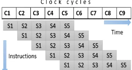
[image:2.612.197.413.598.713.2]The brain behind any electronic system is a processor. RISC machines are designed to fetch, decode and execute a large number of instructions at low clock cycles per instructions (CPI). To achieve such a response, the concept of pipelining comes to use. Pipelining is a mechanism that is used for implementing overlapping execution of several instruction sets by partitioning the computation into a set of sub‐computations (or stages) as shown in Figure 1.
It has a very nominal increase in the cost of implementation with a very significant speedup. The proposed processor has five stages of operation to achieve its desired functionality. They are listed on the next page:
C. Instruction Fetching Stage
[image:3.612.188.412.158.279.2]In this stage, the instruction that is pointed to by the program counter is fetched from the memory and the value of the program counter is incremented to point at the address of the next instruction to be executed.
Figure 2 Instruction Fetching Stage
D. Instruction Decoding Stage
[image:3.612.237.453.348.459.2]In this stage, the queued instruction from the instruction register that is pre-fetched is decoded. It has mainly three or more parts: opcode, operands, and immediate data. There is a parallel execution of the reading the data from the register banks as well as sign extension of immediate data along with the decoding of the instruction in the instruction register.
Figure 3. Instruction Decoding Stage
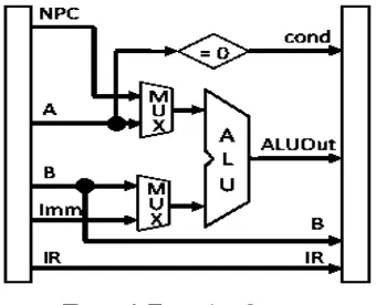
E. Execution Stage
In this stage, Arithmetic and logic unit (ALU) comes into operation. The operation of the value is solely dependent on the decoded instruction. It can be the operations on memory, immediate data or registers. There is a parallel execution of the effective computation of the address that is to be referenced in the memory.
Figure 4. Execution Stage
F. Memory Operation Stage
[image:3.612.226.396.533.671.2]Figure 5. Memory Operation Stage
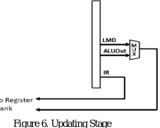
G. Updating Stag
[image:4.612.242.407.244.376.2]In this stage, as the name suggests the processor updates the results from the ALU in the register banks. The value can be either a calculated result of an ALU operation or a data fetch to from memory.
Figure 6. Updating Stage
The 32-bit RISC processor has the following sub-components listed as below:
H. PC
The program counter (PC), also known as the instruction pointer (IP), and sometimes referred as the instruction address register (IAR), the instruction counter, or just part of the instruction sequencer, is a 32-bit special purpose register that points to the next instruction to be executed. In most processors, the PC is only incremented after the instruction is fetched and it retains the memory address of the next instruction that is to be executed.
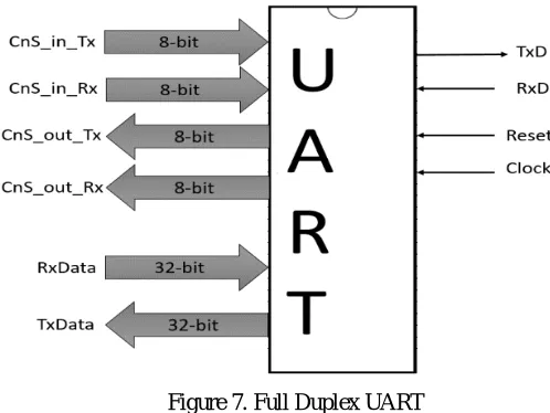
[image:4.612.183.429.475.722.2]The hazards and the race condition between the executions of instructions can be overcome by the help of wait states and master-slave arrangement. Another component of the design is the Universal Asynchronous Receiver and Transmitter described below. UART, which has many different names such as Serial Port, RS-232 Interface, and COM Port etc. is preferably the simplest technique for providing a communication interface with the FPGA. The UART takes in parallel data and transmits the individual bits in a serial fashion. At the receiving end, another UART aggregates the received bits into complete bytes. The rudimentary element of any UART is the shift register for all of its SIPO and PISO conversions. Transmission of serial data through the single channel is preferred over transmission of parallel data across multiple channels. Application-specific chips will cause waste of resources and increase the cost. With the SOC technology increasingly evolving, distinctively in the fields of electronics, the requirement of realizing the system function will be constrained by the over-utilization of chips being used. For coping this problem, designers must integrate the similar function module into FPGA. This design uses Verilog HDL to design and implement the UART operations, and integrate them into an FPGA chip to achieve compact, stable, and reliable data transmission and reception with the RISC machine.
Figure 7. Full Duplex UART
1) Transmitter: The transmitter section generates a sequence of serial data in the frame format. As soon as an input data to be transmitted is detected, a start bit followed by the individual data bits, a 33rd bit (if any), followed by the parity bits(if used) and the stop bits, is sent using TxD.
2) Receiver: The receiver section, on reception of the serial data RxD, identifies the data bytes by segregating the start bit, a 33rd bit(if used), parity bit(if used), and stop bits and stores it in a buffer register for future usage. It verifies if the data byte is preceded by the start bit and followed by the parity and stop bits. The generation is only performed if the given specifications are met otherwise the received data is ignored and rechecked.
3) Control words: There are separate input and output control words that represent the permissions, control signals and updated status flags for the UART operation.
[image:5.612.172.421.238.425.2]Figure 8. Input Control Word for Transmitter
Figure 10. Output Control Word for Transmitter
Figure 11. Output Control Word for Receiver
Figure 12. Flag Description
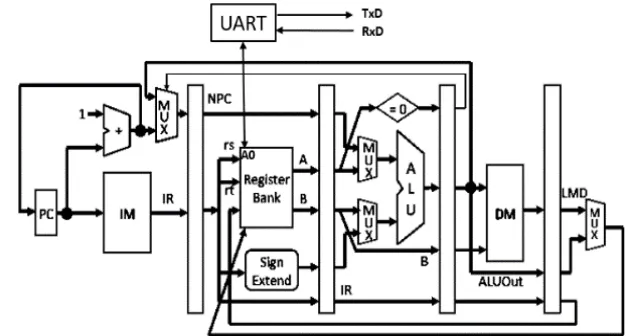
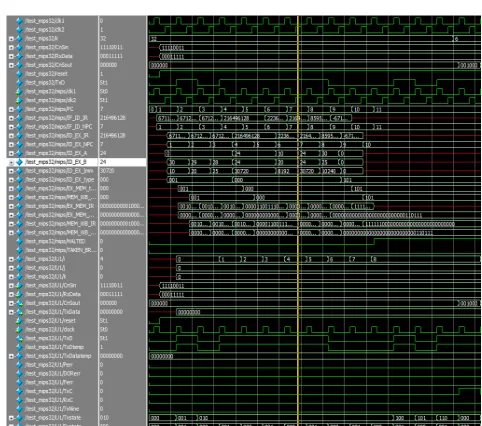
III.IMPLEMENTATIONANDSIMULATION
The fully functional pipelined 32-bit RISC processor is interfaced with a UART for serial data transmission, reception and debug applications using serial monitor. The complete pipelined architecture can be seen in Figure 13 below. The sample program for the testing of the design is also given in Figure 14 on the next page. The timing charts for the 32-bit UART along with the RISC processor is shown in Figure 15 below. The output of individual registers was displayed on the console for proper verification. The contents of the Accumulator register is serially transmitted by TxD along with the additional information (start bit, a parity bit and stop bits). The tools used are ModelSim: Intel FPGA Starter edition 10.5b (Quartus prime 16.1).
[image:6.612.149.464.537.705.2]Figure 14. Sample program
[image:7.612.184.425.500.713.2]Figure 15. Simulation results of UART
Figure 16. Display results of registers on console
IV.SYNTHESIS
A. Selecting an FPGA
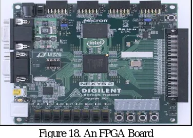
[image:8.612.213.401.171.306.2]The logic synthesis is a process by which an abstract form of desired circuit behaviour, typically at register transfer level (RTL), is turned into a design implementation in terms of logic gates, typically by a computer program called a synthesis tool. Common examples of this process include synthesis of HDLs, including VHDL and Verilog. Some synthesis tools generate bit streams for programmable logic devices such as PALs or FPGAs, while others target the creation of ASICs. In our proposed design, we have used the Xilinx ISE 14.1 for the simulation and the code is downloaded on the Xilinx Spartan 3E CP-132 FPGA Starter board.
Figure 18. An FPGA Board
A field-programmable gate array (FPGA) as shown in Figure 18 is an integrated circuit designed to be configured by a customer or a designer after manufacturing and so the name- "field-programmable". The FPGA configuration is generally specified using a hardware description language (HDL), similar to that used for an application-specific integrated circuit (ASIC). FPGAs contain an array of programmable logic blocks, and a hierarchy of reconfigurable interconnects that allow blocks to be "wired together", like many logic gates that can be inter-wired in different configurations. Logic blocks can be configured to perform complex combinational functions or merely simple logic gates like AND and XOR. In most FPGAs, logic blocks also include memory elements, which may be simple flip-flops or more complete blocks of memory.The synthesis report is shown in Figure 19.
Figure 19. Synthesis report
V. RESULTSANDCONCLUSIONS
A series of multi-level programs were stored in the program memory and the output was observed using the serial monitor and the FPGA. The Accumulator register was able to send and receive data serially through the UART interface and the value of A0 {decimal: 31 as initialized in the sample program} was observed at the serial output TxD and the respective output flags for transmitter was set.
VI.ACKNOWLEDGMENT
[image:8.612.135.490.411.526.2]REFERENCES [1] Advance Digital Design with the Verilog HDL by Michael di Cilleti.
[2] Jikku Jeemon, “Pipelined 8-bit RISC Processor Design using Verilog HDL on FPGA” in IEEE International Conference On Recent Trends In Electronics Information Communication Technology, May 20-21, 2016, India.
[3] Raj Prakash Singh, Ankit K Vashishtha, and Krishna R, “32-bit Re-configurable RISC Processor design and implementation for BETA ISA with inbuilt Matrix Multiplier” in 2016 Sixth International Symposium on Embedded Computing and System Design (ISED).
[4] Agineti Ashok1, V. Ravi2, “ASIC Design of MIPS Based RISC Processor for High Performance” in 2017 International Conference on Nextgen Electronic Technologies
[5] https://www.microchip.com
[6] DKOP Labs Pvt. Ltd.
[7] IEEE Verilog Language Reference Manual 2005
[8] Nathaniel Albuquerque, Kritika Prakash, Anu Mehra, Nidhi Gaur, “Design and Implementation of Low Power Reservation Station of a 32-bit DLX-RISC processor” in 2016 International Conference on Information Science (ICIS).
[9] Suyash Toro1,Sushma Wadar2, Y. V. Chavan3, S C Patil4, D S Bormane5, Avinash Patil6, "External Memory Interface for RISC Controller on Reconfigurable Hardware Logic" in 2016 IEEE International Conference on Advances in Electronics, Communication and Computer Technology (ICAECCT).