Comparative study analysis of Z-source NPC & Z-source T NPC MLI
using SVM
S.Venkatesh
1, K.Gopiteja
2, D.Subba rao
31,2,3
Assistant professor, Department of EEE , KKR & KSR institute of technology & sciences , Guntur, A.P, India
---***---Abstract:
Comparative analysis of a Z-source neutral point clamped inverter & Z Source -T shape - Neutral point Diode Clamped (NPC) - Multi Level Inverter (MLI) power conversion system (Z-T-NPC-MLI) using Space Vector PWM (SVPWM) is presented. This exploits the redundancy switching vector option for both shoot through (ST) and regular switching, which offers a self-control neutral point fluctuation. The conduction losses of the Z-T NPC-MLI are much lower when compared to Z source NPC-MLI. Z-source inverter based adjustable speed drive system effectively uses the shoot-through state to boost DC bus voltage by simultaneously gating on both the upper and lower switches of a same phase leg. The shoot-through zero state has no harmful effect on the inverter and is used to boost the DC link voltage. The adopted approach enables the operation of the Z-source arrangement to be optimized and implemented digitally without introducing any extra commutations. Theproposed techniques are simulated using
MATLAB/SIMULINK & the results are presented. The results shown that the improved harmonic performance of the ULST over the FST strategy and also this simulation results shown that the Z-source NPC inverter Z-T NPC MLI with space vector modulated algorithm is able to boost the output line to line voltage to a value higher than the available dc supply voltage with enhanced sinusoidal output current waveforms.
Index Terms
: Buck–boost, neutral point clamped (NPC) inverter, space vector modulation (SVM), Induction Motor drive, Z-source inverter.I. INTRODUCTION
The inverters are the unavoidable parts in the Photovoltaic systems (PVS), as the output of any PVS will be DC. Many industrial applications require higher power converters (inverters) to drive high power applications. Multilevel converters offer many benefits for higher power applications which include an ability to synthesize voltage waveforms with lower harmonic content [1],[2]. Harmonic performance of the converter plays important role and it is the major factor to synthesize to nearer sinusoidal output. In power systems, lower THD means reduction in peak currents, heating, emissions, and core loss in motors.
The most commonly used topologies are the cascaded inverter [3]–[5], the diode clamped inverter [6], [7], and the capacitor clamped inverter [8]–[10]. Among the above three, the three-level diode clamped [also known as the neutral point clamped (NPC)] inverter has become an established topology in medium voltage drives.
However, the neutral point clamped (NPC) inverter is constrained by its inability to produce an output line-to-line voltage greater than the dc source voltage. The multilevel inverter
Main functions are to produce a desired Alternating current voltage level from several Direct Current voltage sources. The Z-source inverter topology was proposed to over-come the above limitations in traditional inverters. The Z-source concept was extended to the Neutral point clamped inverter in, where two additional Z-source networks which consist of mainly L and C were connected between two isolated dc sources and a traditional NPC inverter. In spite of its effectiveness in achieving voltage buck–boost conversion i.e. both buck and boost.
The space vector modulation approach offers better harmonic and this can more conveniently handle the overall switching patterns. In these inverters, a DC voltage/current source supported by a relatively large capacitor/ large inductor feeds the main three phase bridge inverter circuit. Z-source inverter (ZSI) is a direct current (DC) to alternating current (AC) power conversion concept that is very promising in the fields of power conditioning especially in alternative energy sources and distributed generation and adjustable speed drives (ASD).
II. REVIEW OF Z-SOURCE CONCEPT
Consequently, taking also the PWM modulation index M into account, the phase ac output voltage Vx can be
expressed by (2)
(
) (1)
√ { √ } (2)
where TST and T are the shoot-through interval and
switching period, respectively, B is the boost factor .
Equations (1) and (2) show that the ac output voltage of a Z-source inverter can be regulated from zero to the nor-mal maximum by altering M and maintaining B = 1, or can be boosted above that obtainable with a traditional VSI by choosing B > 1.
III.
TOPOLOGY OF REC Z-SOURCE NPC and Z-T
NPC INVERTER
A. Extension of the Z-Source Concept to the NPC Inverter
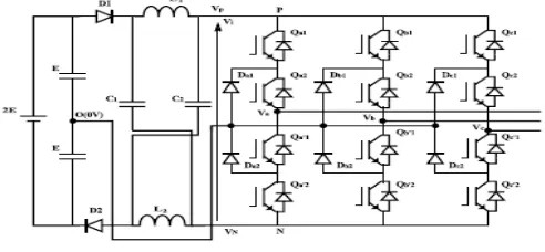
To describe the operating principle of the REC Z-source NPC inverter shown in Fig. 2. The operation of each inverter phase leg of a traditional NPC inverter can be represented by three switching states P, O, and N. Switching state “P” denotes that the upper two switches in a phase leg are gated ON, “N” indicates that the lower two switches conduct, and “O” signifies that the inner two switches are gated ON.
[image:2.595.44.282.278.399.2] [image:2.595.311.557.551.665.2]These extra switching states occur when all the four switches in any phase leg are gated ON [full-shoot-through (FST)], or the three upper switches in any phase leg are gated ON [upper-shoot-through (UST)] or the three bottom switches in any phase leg are gated ON [lower-shoot-through (LST)].
TABLE I SWITCHING STATES OF AN REC Z-SOURCE NPC INVERTER
State
type ON switches ON Diodes Vxo Switching state
NST Qx1,Qx2 D1,D2 +Vi/2 P
NST Qx2,Qx’1 D1,D2,
{Dx1 or Dx2}
0 O
NST Qx’1,Qx’2 D1,D2 −Vi/2 N
FST Qx1,Qx2,Qx’1,Qx’2 — 0 FST
UST Qx1,Qx2,Qx’1 Dx2,D1 0 UST
LST Qx2,Qx’1,Qx’2 Dx1,D2 0 LST
TABLE II SWITCHING TABLE OF Z-T NPC MLI
A. Non shoot through mode:
During the non-ST mode the input DC-link voltage and the inductor voltage together are fed to the inverter which leads to the boosting of the input voltage.
B. Shoot through mode:
However, Full ST state (where all the four switches are ‘ON’ in a leg) is not used in the Z-T NPC-MLI to have independent control on the charging of two inductors (L1 and L2). Hence, the proposed inverter operation uses only top ST (TST) and bottom ST (BST).
C. Circuit Analysis:
The Z-source NPC inverter implemented using a single LC impedance network (see Fig. 2) is considered to be an optimized topology in terms of component count , By controlling the switches of each phase leg according to the combinations presented in Table I, each output phase voltage Vxo (x_{a, b, c}) has three possibilities. Those
possibilities are: Vi /2, 0, −Vi/2.When the REC Z-source
NPC inverter is operated without any shoot-through states, then Vi is equivalent to 2E.
Therefore, to obtain an output line-to-line voltage greater than 2E, shoot-through states are carefully inserted into selected phase legs to boost the input voltage to Vi > 2E before it is inverted by the NPC circuitry. Two
using the FST and NST states is possible, it is generally preferable to use the UST and LST states in place of the FST states (termed the ULST operating mode). The ULST operating mode is preferred because it produces an output voltage with enhanced waveform quality.
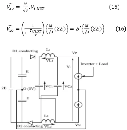
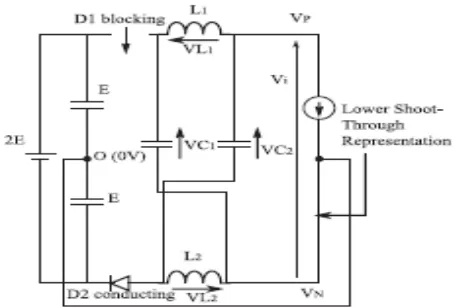
However, the output line-to-line voltage obtained using the minimal loss FST approach has higher harmonic distortion (compared to the ULST approach) in its output voltage wave-form because the voltage levels produced do not have adjacent level switching. The ULST operating mode is used for controlling the REC Z-source NPC inverter. Fig. 3(a) shows the simplified equivalent circuit for the NST state, while Fig. 3(b) and (c) shows the UST and LST states. Assuming that the Z-source network is symmetrical (L1 = L2 = L and C1 = C2 = C), then VL1 = VL2 =
VL & VC1 = VC2 = VC and the voltage expressions for the NST
state are as follows:
No shoot through
(3)
(4)
( ) (5)
Similarly, the voltage expressions for the UST and LST states are as follows:
Upper shoot through
(6)
(7)
Lower shoot through
(8)
(9)
We denote the duration of the NST, UST, and LST states by TN, TU, and TL, respectively, and the switching period by
T. Also, we assume that TU and TL are equal and denote the
total combined UST and LST duration by TU LST. At steady
state, the average voltage across the inductors is zero; therefore, averaging the inductor voltage over one switching period, we have
( )
(10)
(11)
Solving for Vc using (10) and (11), we have
( ) {
} (12)
Substituting (12) in to (5), we have the dc-link voltage Vi during the NST state as
{
} (13)
Similarly, when (12) is substituted into (7) and (9) and noting that Vi = VP − VN , we have the dc-link voltage during
the UST and LST states as
{( )} (14)
It is noted from (13) and (14) that the higher dc-link voltage is present during the NST states The fundamental peak ac output voltage Vxo (x_{a, b, c}) is given b
̂
√ (15)
̂ (
) {√ ( )} {√ ( )} (16)
Fig.3 (a). Simplified representation of REC Z-source NPC inverter in Non shoot through state
[image:3.595.323.545.264.490.2] [image:3.595.319.522.540.703.2]Fig. 3(c). Simplified representation of REC Z-source NPC Lower shoot through states
where B ≥ 1 is the boost factor
IV. MODIFIED SVM OF THE REC Z-SOURCE NPC &
Z-T NPC INVERTER
A. Duty Cycle Calculation
The space vector diagram of a traditional NPC inverter for sector 1 is shown in Fig. 4. The reference vector ⃗⃗ can be expressed as ( ) ( ) ( )
( )
(17)
Generally, in SVM, the ⃗⃗ ref is synthesized with three nearest space vectors, which are selected based on the triangle in which the reference vector is located at the sampling instant. If the reference vector is located in triangle 3, the nearest three vectors are ⃗⃗ 1 , ⃗⃗ 7 , and⃗⃗ 13,
respectively. Let the duty ratios denoted by d1 , d2 , and d3 ,
respectively. The modulation law with a sequence of the nearest three vectors based on the volt–second product is then as follows: ⃗⃗⃗ ⃗⃗⃗ ⃗⃗⃗⃗⃗ ⃗⃗⃗⃗⃗⃗⃗
d1+d2+d3 = 1. (18)
The voltage vectors ⃗⃗ 1 , ⃗⃗ 7 , ⃗⃗ 13, and ⃗⃗ ref in Fig. 4 can be
expressed as ⃗⃗⃗ ( )
⃗⃗⃗⃗ √ ( )
⃗⃗⃗⃗⃗ ( )
⃗⃗⃗⃗⃗⃗ . (19)
Substituting (19) into (18), the duty ratios of the nearest three voltage vectors are given by (20), where M is the modulation index and 0 ≤ θ ≤ π/3. ( )
( ) . (20)
A similar procedure is used for calculating the duty ratios of the selected voltage vectors in all the other triangles.
[image:4.595.49.278.77.231.2]To achieve the minimal number of switches changing between two adjacent states, a seven-segment switching sequence (as in table III) is adopted in SVM.
TABLE III SEVEN SEGMENT SWITCHING SEQUENCE IN TRIANGLE 3
Segment Vector State
E-Null 1 1st V1 ONN
E-Active 1 2nd V13 PNN
E-Active 2 3rd V7 PON
E-Null 2 4th V1 POO
E-Active 2 5th V7 PON
E-Active 1 6th V13 PNN
[image:4.595.69.287.275.445.2]E-Null 1 7th V1 ONN
TABLE IV PERMISSIBLE UST AND LST STATES
Upper Shoot Through states Lower Shoot Through states
UNN PLO
UON POL
OUN PPL
NUN LPO
NUO OPL
NOU LPP
NNU LOP
UNO OLP
ONU PLP
[image:4.595.314.549.572.713.2]normalized volt–second area applied to the load is unchanged from the standard NPC case discussed above. Note that when any phase has UST applied, the positive rail (P) is at the same potential as the dc mid-point (O). Similarly, during LST, the negative rail (N) is at the same potential as the dc mid-point (O). Consequently, it is only possible to use the UST state on a given phase when it is connected to O and the other two phases are connected either to O or N in order to get the correct line-to-line voltages. Similarly, an LST state can only be used when the other two phases are O or P. Therefore, the permissible shoot-through states are as shown in Table IV where “U” and “L” represent UST and LST states in a phase leg, respectively. Fig. 5(a) shows the seven-segment PWM switching sequences for modulating a traditional NPC inverter and an REC Z-source NPC inverter when the reference vector, ⃗⃗ ref is in triangle 3 of the vector diagram shown in Fig. 4.
FIG. 5(a) Modulation of traditional NPC and Z-source NPC when the reference vector is in triangle 3on the three
level vector diagram shown in Fig.4.
FIG .5(b) Modulation of traditional NPC and Z-source NPC when the reference vector is in triangle (4) on the three
level vector diagram shown in Fig.4.
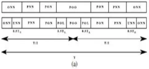
Comparing the sequences shown in Fig. 5(a), it is observed that the only difference between them is the insertion of a UST state in phase A to the left of the E-active state {PNN} and the insertion of an LST state in phase C to the right of the E-active state {PON}, respectively, within half switching period, T/2. The process is reversed in the remaining half switching period. The phase Applying the same analysis and moving on to the second transition ({PNN} to {PON}), where phase B switches from the “N” state to the “O” state, no
[image:5.595.305.561.222.303.2]shoot-through state is inserted (note that it is not possible to introduce UST or LST for the {PON} state for the reasons discussed earlier).Moving forward again to the third transition ({PON} to {POO}) where phase C switches from the “N” state to the “O” state, an LST state is inserted since the switching of devices {Qc1,Qc2,Qc_1,Qc_2} from {OFF, OFF, ON, ON} through {OFF, ON, ON, ON} to {OFF, ON, ON, OFF} will not affect phases A and B, which remain clamped to points P and O.
TABLE V SWITCHING SEQUENCES AND INSERTION OF SHOOT –THROUGH STATES IN TRIANGLES 2-4
Triangle Switching Sequence
2a {ONN} {UNN} {ONN} {PON} {POL} {POO}
2b {PPO} {PPL} {POO} {PON} {UON} {OON}
3 {ONN} {UNN} {PNN} {PON} {POL} {POO}
4 {OON} {UON} {PON} {PPN} {PPL} {PPO}
The previous methodologies is applied to another distinct triangle, triangle 2a, a similar state sequence is derived and shown in Fig. 5(b). From the above, it is noted that in all triangles, the UST (or LST) states are inserted at the “E-Null” to “E-Active” state transitions with no shoot through states inserted at the “E-Active” to “E-Active” state transitions. Another feature noted with the ULST modulation scheme is that the UST and LST states are introduced for only half of the total shoot-through duration of TULST, unlike the FST modulation scheme,
where the Z-source network is shorted for the full shoot-through duration. Therefore, to produce the same boost factor for the ULST and FST schemes, we need to set TULST/T = 2TFST/T, where TFST is the FST duration. The
available shoot-through period is limited by the E-null period that is determined by the modulation index.
(21)
Table V gives a summary of the above discussions when the reference vector is in the various triangles of sector 1. However, it should be noted that in triangle 1, no shoot-through states are inserted because this corresponds to a low modulation index.
PROPOSED SVPWM SCHEME FOR Z-T NPC MLI
For a Z source NPC-MLI the conventional Z source SVPWM scheme uses 54 ST-states. The new proposed SVPWM scheme uses only 24 ST-states in addition to maintaining the capacitor balancing along with 27 regular switching states [3-Zero vector (ZV),12-small vector (SV),6- medium vector (MV) and 6 large vector (LV)]. Basically the MLI Z-source SVPWM schemes differ from MLI, only by adding the ST switching states. This is because, Z-Source NPC-MLI needs ST vectors to charge the inductors present in Z-network.
[image:5.595.40.281.302.414.2] [image:5.595.40.284.478.597.2]V. SIMULATION RESULTS
[image:6.595.314.553.109.209.2]In this simulation platform, a standalone three-phase induction motor was used to verify the theoretical findings. To demonstrate the boosting ability of the REC Z-source NPC inverter, first, a modulation index, M of 0.825. The inverter dc-link voltage is obviously not boosted and the peak value of the output line-to-line voltage is maintained at almost 400V by the dc source. High-quality sinusoidal line currents are also observed.
TABLE VI COMPARISON OF ULST AND FST STRATEGIES
Parameters FST Strategy ULST Strategy
Total harmonic distortion 29.27% 28.39%
Commutation count 4 2
Switching loss High Low
The simulation results show that the REC Z-source NPC inverter, with the proposed SVM algorithm, is able to boost the output line-to-line voltage to a value higher than the available dc supply voltage with sinusoidal output currents.
To show the improved harmonic performance of the ULST strategy over the FST strategy, simulations using the FST strategy were also carried out with the same parameters as those of the ULST strategy (except that TFST/T = 0.175 = 0.35/2) and the results shown in Fig.7.2
and Fig.7.3. Table V gives a comparison of the performances of the ULST strategy, non minimal loss FST, and the minimal loss FST strategies. Also, to show that the UST and LST states do not introduce any significant harmonic distortion to the output line-to-line voltage, the same dc-link voltage was used for the non boost mode (i.e., 2E = 120 V, TULST/T = 0) and the boost mode (2E =
120/1.53 V, TULST/T = 0.35) and their harmonic
performances compared as shown in Fig. 9
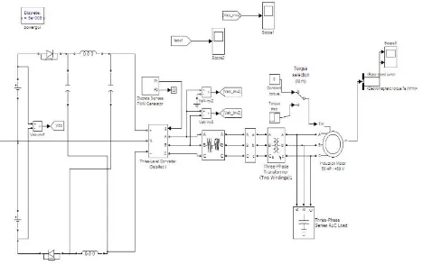
Fig.6.1.Simulink model for Carrier UST based Induction Motor.
The MATLAB/Simulink model of proposed Z-source REC three level Neutral point clamped inverter with carrier UST state is shown in the figure 5.1. In this, the input of the three level converter is a diode clamped
multilevel inverter. Typically m-level inverter consists of m-levels on the phase voltage.
Fig.6.2 (a) Three Phase Voltages Vab,Vbc,Vca & phase to neutral voltage Van
The waveforms of phase to phase voltage Vab (V) is
shown in the above figure 6.2(a).The Output of the line voltage results three-level stair case.
Fig.6.2 (b) Three Phase currents (Iabc)
The waveforms of a three phase currents Iabc(p.u) shown in above figure 6.2(b) and the enhanced
three phase current waveforms obtained is nearer to sinusoidal with less harmonic content
[image:6.595.311.556.294.418.2]Fig.6.2(c) Voltage THD in %
Fig.6.2 Simulated waveforms of REC Z-source NPC inverter using Carrier UST strategy
[image:6.595.308.559.498.648.2] [image:6.595.42.276.534.681.2]Fig.7.1 Simulink model for FST,ULST based Induction Motor.
Fig.7.2 (a) Three Phase Voltages Vab,Vbc,Vca & phase to neutral voltage Van(volts)
The obtained three phase voltages is shown in the below figure 7.2(a). The waveforms shows the Vab, Vbc , Vca
, Vzn and from the output waveforms, a 3-level stair case
enhanced waveforms obtained .
Fig.7.2 (b) Three Phase currents (Iabc)
The Full shoot through obtained current waveforms is shown in the above figure 7.2(b). From the waveforms, the obtained three phase currents are sinusoidal and also got enhanced quality current waveforms.
Fig 7.2(c) Voltage THD in %
Fig.7.2 Simulated waveforms of REC Z-source NPC inverter using Carrier UST strategy.
[image:7.595.51.287.79.231.2]The simulation results for the full through switching state is presented above and the the total harmonic distortion is reduced as shown in the figure 7.2(c) which is a shoot through state and in this state the upper and lower switches in the phase leg are triggered. In this full shoot through state, the harmonic distortion values are greatly reduced in this and the obtained value is 29.27%.
Fig.8.1 Simulink model for ULST based Induction Motor
Fig.8.2 (a) Three Phase Voltages Vab,Vbc,Vca & phase to neutral voltage Van.
The output of the line-to-line voltage results a three level stair case waveforms.
Time (sec)
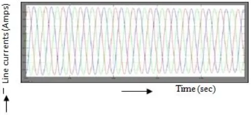
Fig.8.2 (b) Three Phase Currents (Iabc)
Line
c
u
rr
en
ts (A
m
p
[image:7.595.41.278.277.410.2] [image:7.595.319.556.427.569.2] [image:7.595.38.283.516.632.2] [image:7.595.311.540.644.746.2]The upper lower shoot through obtained current waveforms is shown in the above figure 8.2(b). From the waveforms, the obtained three phase currents are sinusoidal and also got enhanced quality current waveforms.
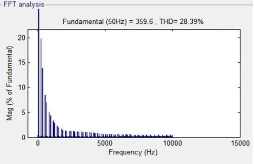
[image:8.595.312.555.76.384.2]Fig.8.2(c) Voltage THD in %
Fig.8.2 Simulated waveforms of REC Z-source NPC inverter using Carrier UST strategy.
The simulation results with the combination of upper and lower shoot through switching state is presented above figure 8.2(c). The harmonic distortion values are greatly reduced in this and the obtained value using this strategy is 28.39%.
The total harmonic distortion (THD) of the output line-to-line voltage is compared to that of the proposed SVM strategy in Table VI.
TABLE VI COMPARISON OF THD OF THE PROPOSED SVM AND CARRIER-BASED PWM WITH
ZERO-SEQUENCE VOLTAGE INJECTION.
Mode Proposed SVM Optimised carrier-based PWM
Non boost Mode 49.54% 37.47%
ULST Mode 28.39% 36.81%
From Table VI, it can be concluded that the harmonic performance of the proposed SVM strategy is comparable to the carrier-based PWM with zero-sequence voltage injection strategy described in [20] and hence is a competitive alternative for modulating the Z-source NPC inverter.
(b)
Fig.9. THD of Z-T NPC MLI
CONCLUSION
A novel Z-T NPC MLI is implemented using the new SVPWM scheme and operated in the entire modulation region both in shoot through mode and non-shoot through mode. This proposed SVPWM scheme uses redundant technique, which provides the equal switching stress to all the phases which improves the performance of the inverter for long operations.
In this paper, the simulation of three level multilevel inverter is carried out in MATLAB/ Simulink, to identify the suitable level inverter which has comparatively less total harmonic distortion in its output. The total harmonic performance of ULST and FST strategies with the same dc-link voltage. A comparative study is done for better configuration of multilevel inverter. A modified SVM for an REC Z-source NPC inverter is presented. The insertion of the shoot through states was such that the number of device commutations was kept at a minimum of six per sampling period, similar to that needed by a traditional NPC inverter.
REFERENCES
[image:8.595.37.288.143.305.2][2] J. Zhao, Y. Han, X. He, C. Tan, J. Cheng, and R. Zhao, “Multilevel circuit topologies based on the switched-capacitor and diode-clamped converter,” IEEE Trans. Power Electron.,vol. 26, no. 8, pp. 2127–2136, Aug. 2011.
[3] P. Sun, C. Liu, J.-S. Lai, and C.-L. Chen, “Cascade dual buck inverter with phase - shift control , ” IEEE Trans. Power Electron., vol. 27, no. 4, pp. 2067–2077, Apr. 2012.
[4] J. Ebrahimi, E. Babaei, and G.Gharehpetian, “Anew topology of cascaded multilevel converters with reduced number of components for high - voltage applications , ” IEEE Trans. Power Electron., vol. 26, no. 11, pp. 3109– 3118, Nov. 2011.
[5] C. Govinda raju and K. Baskaran , “ Efficient sequential switching hybrid modulation techniques for cascaded multilevel inverters,” IEEE Trans.Power Electron., vol. 26, no. 6, pp. 1639–1648, Jun. 2011.
[6] J. Shen, S. Schroeder, R. Roesner, and S. El-Barbari, “A comprehensive study of neutral-point self-balancing effect in neutral – point -clamped three level inverters , ” IEEE Trans. Power Electron., vol. 26, no. 11, pp. 3084– 3095, Nov. 2011.
[7] J. Li, J. Liu, D. Boroyevich, P. Mattavelli, and Y. Xue, “Three level active neutralpoint clamped zero -current-transition converter for sustainable energy systems,” IEEE Trans. Power Electron, vol. 26, no. 12,pp. 3680–3693, Dec. 2011.
[8] T. Meynard and H. Foch, “Multi-level conversion: High voltage choppers and voltage-source inverters,” in Proc. Conf. Rec. 23rd Annu. IEEE Power Electron. Special. Conf., Jul. 1992, vol. 1, pp. 397–403.
[9] S. Thielemans, A. Ruderman, B. Reznikov, and J. Melkebeek, “Improved natural balancing with modified phase-shifted PWM for single-leg fivelevel flying-capacitor converters,” IEEE Trans. Power Electron., vol. 27, no. 4, pp. 1658–1667, Apr. 2012.
BIOGRAPHIES
S.Venkatesh received B.tech (EEE) From jntu, anantapur in the year (2007-2011) and M.tech (Power Electronics) in Narayana Engineering College, Gudur, A.P , India (2012 – 2014). He is currently working as Assistant Professor in the department of Electrical and Electronics Engineering at KKR&KSR Institute of Technology and Sciences , Guntur Dist, Andhra Pradesh , India. His research areas include Power Electronics and Electric Drives.
K.Gopiteja received B.tech (EEE) From jntu, Kakinada in the year (2006-2010) and M.tech (Control systems) in St.Marys College of engineering and technology, Hyderabad , Telangana , India (2011 – 2013). He is currently working as Assistant Professor in the department of Electrical and Electronics Engineering at KKR&KSR Institute of Technology and Sciences , Guntur Dist, Andhra Pradesh , India. His research areas include Power Electronics and Control systems.