A
FULL
CUSTOM
MAC
USING
DADDA
TREE
MULTIPLIER
FOR
DIGITAL
HEARING
AIDS
1ANANDI. V , 2DR. RANGARAJAN . R
1
A Associate Professor, ECE Dept,
Department of ECE , M S Ramaiah Institute Of Technology Bangalore INDIA
2
A Principal, Indus Engineering College, Coimbatore , INDIA
E-mail: [email protected]@gmail.com
ABSTRACT
The ultra-low power requirements of emerging implantable and wearable biomedical devices, necessitates, novel power management schemes. In this paper, we focus our attention on large DSP data path operators such as multipliers and MAC circuits, where lowering the energy per operation is of greater importance. These form the heart of a majority of commercial DSP Processor data path units. We examine architectural choices for merged MAC circuits and formulate a high-speed/low-power MAC architecture.An efficient hardware architecture for Multiply Accumulate (MAC) unit based on a modified Dadda tree multiplier is proposed and validated in full custom environment in standard cell 180nm technology. The partial products reduction block is completely designed using the novel binary compressors and the addition module is implemented using a new less complex modified full adder based on XNOR. Feeding the bits of the accumulated operand into the summation tree before the final adder helps to increase the speed .The final adder is implemented using ripple carry adder. The resulting MAC is implemented and compared with the existing low power designs. The simulation results show that the proposed implementation is faster and consume less power than similar implementations making it a viable option for efficient designs. The 32x32 bit MAC unit designed using proposed full adder as the basic building block gave a power saving of 24.27% over 32 bit MAC designed using SERF full adder and 35.07% power savings over 32 bit MAC designed using conventional 28T full adder.
Keywords: Wallace, Compressor, Low power, MAC, SERF full adder,
1. INTRODUCTION
The application domain we are considering: audio signal processing and more specifically digital hearing aids has replaced the analog signal processing circuit with a digital signal processor (DSP) for increased signal processing capabilities. Because hearing aids have extremely low power
consumption requirements of total power
consumption in the order of 0.5 - 1.0 mW (at 1.0 V supply) many commercial hearing aids are based on hardwired ASIC solutions[1]The lifetime of the battery is often the more pressing concern to the consumer. As these battery-powered mobile applications push for flexible and low-power system-on-chip solutions, there is a necessity to
design energy efficient domain specific
DSPs.Therefore the need is to optimize DSP architectures with an application domain in mind i.e., to design domain specific DSPs. The objective of this work is to design energy efficient full custom based 32 x32 bit MAC unit to be used in modern day DSP processors which are part of any
digital hearing aids. The objective is achieved by designing a pass transistor based full adder using signal gating for low power operation which is in the critical path of any multiplier. The proposed design of the MAC uses a modified dadda tree multiplier with column compression to speed up the partial product summation stage The combined low power adder with faster tree structure of the multiplier is responsible for the energy efficient and
lower delay of the proposed MAC unit. The
describes the design and implementation of a 32-bit multiply-accumulate unit with 31:5 compressor and final ripple carry adder. Finally, Section 6 discusses the results of the proposed MAC design with classic static CMOS design in terms of delay and power dissipation. Section 7 concludes the paper with scope for future work.
2 .
GENERAL CONSTRUCTION OF MAC UNIT
The general construction of the MAC operation can
be presented by this equation Z = X X Y + P
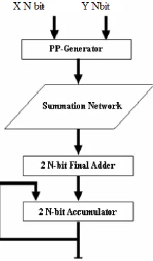
[image:2.595.235.505.75.319.2]Where the multiplier X and multiplicand Y are assumed to have n bits each and the addend Z has (2n+1) bits. The basic MAC unit is made up of a multiplier and an accumulator and a merged MAC as shown in Fig. 1, 2.The multiplier can also be divided into the partial products generator, summation tree, and final adder. This construct leads to four basic blocks to implement. The summation network represents the core of the MAC unit. This block occupies most of the area and consumes most of the circuit power and delay. Several algorithms and architectures are developed in attempt to optimize the implementation of this block.
[image:2.595.113.262.442.696.2]Figure 1: Regular MAC
Figure 2: Merged MAC
Low-power DSP’s intended for audio applications include designs with a variety of full-custom circuit techniques, [2]and some of them even use
dual Vt processes to obtain high speed and low
standby power consumption at the same time. The Coyote processor developed by GN Resound and Audio logic [3] resembles a general-purpose DSP architecture and has a specialized instruction set that displays high parallelism and a datapath with a special multiply accumulate unit called PMAC.[4]. An approach to speed up the operation of MAC is to implement both the multiplication and the accumulation operations within the same functional block by merging the accumulator with the multiplication circuit. Many researchers have attempted in designing MAC architecture with high speed and low power consumption either with a fast pipelined implementation to lower the MAC architecture’s critical delay [5] or half array implementation to design a high-speed and area-effective MAC architecture [6]. A low-power MAC unit using the radix-4 Booth algorithm, by
reducing its architectural complexity and
Wallace & Dadda’s scheme) [11],[12],[13] and array-based structures[14] are more useful for their respective high speed and regular layout.
3. POWER DISSIPATION IN MULTIPLIERS
Multipliers are often found in the critical path of signal processors and are large block of a computing system [15],[16]. Not only is the multiplier a high delay block, but it can be a significant source of power dissipation. Energy efficient parallel multiplier design requires the exploration of many application algorithms, technology constraints and circuit implementation techniques. In general, the multiplier can be divided
into three categories: i. Serial form ii.
Serial/Parallel form iii. Parallel form .The design of low-power multiplier involves the i. complexity of the multiplier area which is quadratically related to the operand precision. ii spurious transitions or glitches due many logic levels in the parallel multipliers iii.The complex structure of parallel multipliers deteriorating the efficiency of layout and circuit level optimization. The speed of the multiplier is determined by both architecture and circuit and dependent on number of the cell delays along the critical path, ( a delay of an adder), and is determined by the design of the circuit of the cell.
There are three categories of multiplier
architectures studied in terms of power
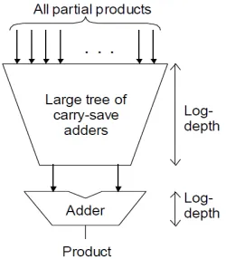
[image:3.595.130.255.521.664.2]consumption: 1.Array Multiplier 2.Tree Multiplier 3.Booth Recoded Multiplier. In terms of power dissipation, the tree-based structure is lower power than the array-based structure. [17].
Figure 3 : Full Tree Multiplier
3.1 Low Power Multiplier Structures 3.1.1 Partial Products (PP) Generation
Radix Multiplication consists of generating the product of two numbers the multiplicand and the multiplier. Accumulation is the iterative addition of
the multiplication results over all input vectors. The most efficient multiplier structure will vary depending on the throughput requirement of the application. The parallel multipliers consist of three main computational blocks namely partial product array(PPA), partial product reduction(PPR) and final addition(FA).In the binary systems, an AND gate can be used to generate partial product. The PPA bits generated via logical AND are created in parallel hence the static delay of each of the bits is equal. Also, the dimensions of the array are functions of the multiplier and multiplicand size: the height and the width of the array are proportional to the size of the multiplier, and the size of the multiplicand respectively. Finally, all the bits in a particular column are to be added together, and some columns have fewer bits than others especially high-order and low-order bit positions will require fewer additions than the middle bit positions .After the partial product generation block, the partial products will be reduced to two rows, a row of sum and a row of carry signals. The final step is the addition of the generated carry and sum signals. In full tree architectures, there is variation in i.partial product generation circuits which can be a collection of AND gates (i.e. a AND
xi)or in signed Booth multipliers, these are Booth
recoding block [17] ii. Partial Products Reduction Tree which is usually a carry-save tree (i.e. Wallace, Dadda) producing a "redundant" result (i.e. carry and save outputs) iii. Redundant-to-Binary Converter usually a fast carry-propagate adder CPA.[18], [19], [20] .
3.1.2 Partial Products (PP) Reduction:
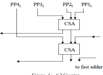
][23],[24] The reduction process is performed with either an array topology or a (Wallace) tree topology using a CSA array using the basic elements. Array structures use carry-save additions in a sequential manner, whereas Wallace trees perform carry-save addition in a parallel manner. A sequential carry-save procedure will reduce the number of bit vectors by one at each stage. A tree of carry save adders is called a “Wallace tree”. Only 2 levels of CSA are needed in the Wallace tree for 4 partial products whereas the linear structure requires 3 levels. The number of stages, and hence the delay of the sequential operation will be O (n) and a regular structure, enabling easy layout. Wallace trees employ a parallel reduction scheme and have a logic depth of O (log3/2n), but an irregular structure making it difficult to layout. A high-speed carry-propagating adder is used to produce the final result from the two rows. The horizontal lines indicate that the carry out must be passed to the next most significant bit slice. Since we make each bit slice the same, there will also be a corresponding carry in. Fig 4
Figure 4 : 4:2 Counter
3.1.2.1 Wallace tree versus Dadda tree:
Wallace introduced a scheme for fast multiplication based on using parallel “pseudo adders which is (3,2) counter. The main advantage of the (3,2) counter is that it avoids carry propagation. (3,2) and (2,2) counters are then employed within each three row set. During the reduction process, each (3,2) counter takes three inputs from a given column and outputs a sum bit which remains in that column and a carry bit which enters the next more significant column. Dadda later refined Wallace’s method by defining a counter placement strategy that required fewer counters in the partial product reduction stage at the cost of a larger carry-propagate adder. For both methods, the total delay is proportional to the
logarithm of the operand word-length.In Wallace
tree after partial products are created, they are summed together to reduce number of operands as
[image:4.595.351.458.375.507.2]soon as possible, 4 x 4 example Fig 5 below .The first step is to rearrange the partial products according to bit positions as shown in Figure The longest path consists of 4 terms at bit position 3. The final step is to determine the number of half and full adders required to complete the addition operation. In Dadda tree combine the pps as late as possible while maintaining same number of carry-save levels (tree height) Fig 6 .
Figure 5 : Wallace tree reduction
Figure 6 :Dadda Tree Reduction
[image:4.595.92.273.393.525.2]Figure 7 : 9-Input CSA Reduction Tree
3.1.2.2 Compressors :
A p:q compressor consolidates N input bits in the kth column to 2 output bits, with one bit output in
the kth column and one bit for each of the next q-1
columns. Additionally, there are L carry-in bits
[image:5.595.92.304.105.352.2]entering the compressor at different levels and also L carry-out bits leaving the compressor at different levels as shown in Fig 8.In the MAC design, for high throughput operation, the result of partial product reduction can be fed back directly to the next cycle in a carry-save form. In this case, a new method can be used to eliminate one row of the partial product matrix before the actual reduction process begins, which can eliminate one 3:2 counter delay for some specific operand sizes. Overall, the new design is 14.3% faster in terms of XOR delays for the partial product reduction. [26].
Figure 8: Simple Compressor
[image:5.595.307.505.307.458.2]A [4:2] compressor can also be designed using two [3:2] compressors as shown in Figure 9.
Figure 9 :4 : 2 Compressor
Complex compressors or binary trees can be built by using basic compressors like [3:2] and [4:2] compressors which makes the layout problem much easier. Fig 10.
Figure 10: 8:2 Compressor
If we decompose each (4,2) block into (3,2) elements, there are 2 stages of (3,2) elements in each (4,2) block. This gives a total of 4 stages for 8 partial products in both designs (same delay) which is much better than the 7 required for the linear structure. The layout for the tree with (4,2) building blocks is probably more straightforward than using (3,2) elements directly as building blocks. Remember, each bit slice of the tree must be repeated N times. Fig 10 . The carry save adder can be regarded as the most general circuit that takes some number of inputs and represents the sum of the inputs in 2 binary weighted output bits. We can extend this idea into larger building blocks that represent binary weighted sums in 3, 4 or more bits. (3,2): most inputs in 2 output bits
(7,3): most inputs in 3 output bits (15,4): most inputs in 4 output bits
[image:5.595.98.280.570.702.2]more efficient even if the (7,3) block is constructed from (3,2) blocks. [28] . A similar organization is obtained using (15,4) as a building block. But it is difficult to easily route the 15 inputs to this single block. It requires numerous feed throughs in the partial product generator. Likewise a [11:2] compressor can be built using three [3:2] , two [5:3] and one [4:2] compressors Fig 9.Based on property of counter, a 15-4 compressor is constructed using eleven full adders.
[image:6.595.120.271.246.464.2]Figure 11 :11: 2 Compressor
Figure 12: 16:2 Out Of 7:3 And 4:2
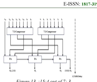
A 15:4 reduction tree obtained using two 7:3 compressors, three 3:2 counters is implemented in this paper. Fig 13
Figure 13 :15:4 out of 7: 3
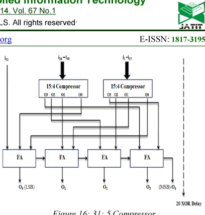
In this paper, a new fast 31:5 compressor is
proposed for high-performance multiplier
implementation using the 15: 4 blocks. The new fast compressor is obtained by applying adder cells in parallel and a new logical decomposition is used for fast implementation of the 1 bit adder. In hybrid CMOS implementations, a 3:2 counter is implemented with 1-stage modified SERF logic [29] In the new logical decomposition, the 1-bit adder cell has 2 XOR delays on the critical path.
[image:6.595.323.482.398.694.2]Figure 14: Schematic Of Proposed Full Adder
Figure. 15: Proposed 3: 2 Counter
3. 3 Final Addition
The two 2n-1-bit reduced partial product vectors
[image:6.595.89.281.469.643.2]reduction stage in order to exploit the tree’s logarithmic compression depth. A number of alternatives exist for the final CPA, varying in the speed, area and complexity. There exist many architectural choices for final addition like Block Carry Look ahead Adders which use a parallel tree structure for rapid addition with a gate depth of
O(log2n), and is one of the most popular choices
for high-speed/low-power final adders. Alternative solutions are parallel prefix adders, which offer close to logarithmic delay. An RCA or a Manchester adder has the area and worst case delay
proportional to the adder’s length. The ripple adder
is the slowest yet lowest power adder
implementation. Therefore the speed and power properties of the ripple adder determine the overall performance of a wide range of adder designs. As can be seen, the delay is linear in the number of addition stages.[30] .
4. 32-BIT × 32-BIT MAC DESIGN:
4 .1Architecture of a MAC Using the New 31:5 Compressor
To reduce the number of partial products, high-throughput operation, the accumulator stores an intermediate result in a carry-save form and the accumulator output is fed back for the next accumulation operation. In this manner, carry propagating addition is separated from the critical path in MAC operation. The partial products and accumulator output are combined to form a partial
product matrix and undergo 15:4reduction
processes. In the 32-bit by 32-bit MAC design, the new 31:5 compressor block is used and it was shown that it effectively eliminates one XOR in the partial product reduction. A 31:5 Compressor is a combinational logic circuit that accepts 31 inputs and gives out 5 outputs. Where i1-i31are inputs of counter and the three outputs are O4, O3, O2, O1 and O0 where O0 is the LSB and O4 is the MSB. Based on property of counter, a 31-5 compressor is as shown in is constructed using eleven full adders.
It takes 20XOR instead of 21XOR delays in a
[image:7.595.303.507.76.290.2]conventional design, which is 14.3% speed improvement.
Figure 16: 31: 5 Compressor
[image:7.595.305.507.327.477.2]A 4:2 compressor is implemented with two cascaded full adders.
Figure 17 : 4:2 Compressor Hybrid CMOS Logic
Table 1 PDP Comparison For Low Power Full Adders [30]
Table 1 shows the circuit simulation result of power and delay using highly customized hybrid CMOS
circuit implementation in 0.180 µm bulk CMOS
technology for the proposed adder. The parameters of power dissipation and delay are compared with
Full Adder Designs
Power in uW
Delay in pS
PDP in Fj
EDP(10 -2 4
J-sec)
CMOS 28T FA 46.43 208.70 9.6914 2.0225.
Optimized TG FA 46.91 51.46 2.4142 0.1242
SERF FA 39.12 39.02 1.5264 0.0595
the Static and hybrid CMOS adders existing in literature. [31] [32] .An early analysis on power Performance of the multiplier identifies that adder levels have the major portion of power consumption. Approximately 400 input patterns are applied to the proposed adder to verify its functionality. Simulation results using CADENCE SPECTRE show that our adder can operate at 100 MHz in 0.18 μ CMOS technology under the supply voltage of 1.8 V.
Figure 17 : Input And Output Test Patterns
In this paper, a new 31:5 compressor is implemented to achieve 32-bit by 32-bit MAC design. In general, the 31:5 compressors can be used for other multiplication or multiply-addition applications. For maximum performance, 3:2 counters are used whenever 3 or 4 rows are left even after the application of 7:3 compressors. The performance is mainly determined by compressor cell design. In addition, the performance can be different depending on specific operand sizes because the use of a specific compressor leads to a specific sequence of maximum numbers of rows to be handled. The Wallace tree performs especially well when the number of rows is 6, 9, 37–42 and 59–63. The binary tree is good when the number of rows is 4, 14–16 and 59–64. In these methods, the reduction architecture and its delay is determined by the tallest vertical bit slice in a PPM (partial product matrix). The logic elements and their interconnections in the vertical slice is replicated to different bit positions. This approach has been
widely used in fully customized circuit
implementations of large multipliers where interconnection complexity and design modularity are major design bottlenecks. One of recent works
[image:8.595.309.487.254.435.2]on partial product reduction is to use an algorithmic approach utilizing delay difference of carry and sum outputs to attain maximal performance. The 7:3 compressor is a combinational logic circuit that accepts 7 inputs and gives out 3 outputs. It uses four full adders in its design. The full custom Layout design for the 7:3 Compressor was done using Virtuoso XL editor. Post Layout Simulation (stimuli test bench) is performed on the extracted layout, and the results were verified to be working satisfactorily.
Figure 18 : Full Custom Layout Of 7:3 Compressor
Figure 19 : 15: 4 Compressor Using Proposed Adder
[image:8.595.314.498.461.616.2]Table 2 : Low Power Compressors
5.0 MAC LOGIC IMPLEMENTATION
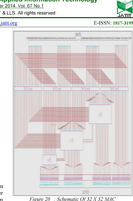
Using 16x16 multipliers, 32x32 multiplications can be executed. The 64 bit output of 32x32 multiplier is interpreted as W X Y Z, with each of them exhibiting 16 bits output. We now perform 16 bit multiplication in the form: A = A31-A16, (MSB1) A15- A0, (LSB1) ,B31-B16,(MSB2),B15-B0 (LSB2).Now using 16x16 multiplication outputs, we compute W, X, Y and Z .
Finally the 64 bit output (S63 to S0) of 16x16 multiplier is represented by WXYZ each of them
have 16 bit length.
Figure 20 : Schematic Of 32 X 32 MAC
Only after passing the DRC check with no errors and matching perfectly with LVS pass, the parasitic of a layout is extracted.
6. ANALYSIS AND DISCUSSION
This paper described a design of an efficient 32 X 32-bit MAC unit. An early analysis on power performance of the multiplier identifies that adder levels have the major portion of power consumption. Approximately 400 input patterns are applied to the multiplier to verify its functionality. Simulation results using CADENCE SPECTRE show that our multiplier can operate at 100 MHz in 0.18 μ CMOS technology under the supply voltage of 1.8 V. Approximately 400 input patterns are applied to the multiplier to verify its functionality. All 3 MACs have been simulated using a common test setup in Cadence®. A variety of test vectors are applied at the input ports and the resulting outputs are analyzed using SPECTRE waveform window. The power is calculated by finding the average current and multiplying it with the supply voltage. Compressors Power
in uW
Delay in pS
PDP in fJ
EDP( 10 -24
J-sec) 4:3
Compressor 28.16 464.7 13.0859 6.0810
5:3
Compressor 32.81 475.9
5
15.6159 7.4323
6:3
Compressor 43.14 606.4
5
26.1622 15.8660
7:3
Compressor 44.80 689 30.8672 21.2675
15:4
Compressor 248.78 1205 299.779
9
361.2347
31:5
Compressor 322.6 2015 650.039 1309.8285
LSB2 x LSB1
LSB1 x MSB2
MSB2 x MSB1
MSB1 x LSB2
W1 W2
W3 W4
W7 W8
[image:9.595.92.235.473.558.2]Figure 20 : Simulation Set Up
[image:10.595.84.514.483.761.2]The conventional 32 x 32 bit MAC using static CMOS has a delay of 39.81 ns with 43.88 mwpower dissipation at nominal power supply (1.8 V). The proposed structure with its more complex PPG resulted in 7.25ns delay and 28.49mW power dissipation at nominal supply with 35.07% power savings.Calculating the power delay-product (PDP) for the two architectures at nominal supply gives 1747.9pJ and 206.55pJ for the conventional and proposed, respectively. The 32 bit MAC designed using proposed full adder, is compared against 32 bit MAC units designed, using conventional 28T full adder as its basic building block and using SERF full adder as its basic building block for performance. (Table4). The 32x32 bit MAC unit designed using proposed full adder as the basic building block gave a power saving of 24.27% over 32 bit MAC designed using SERF full adder and 35.07% power savings over 32 bit MAC designed using conventional 28T static CMOS full adder.
Table 4 : Proposed Mac Performance
Table 5 : Mac Comparison
7 .0 CONCLUSION
In this paper, energy-efficient 32 bit multiply and accumulator (MAC) unit architecture has been presented. The architecture is based on reduced complexity modified Wallace tree architecture for optimal performance. In this paper, a new fast 31:5 compression method is derived from a fast 1-bit adder cell. The 1-bit adder cell has better delay of performance when new logical decompositions used. In addition, its hybrid CMOS circuit is
proposed for highly customized design
methodology. For the partial product reduction of a 32-bit by 32-bit MAC, the use of the new compressor cell leads to 14.3% speed improvement in terms of XOR delay.The 32x32 bit MAC unit designed using proposed full adder as the basic building block gave a power saving of 24.27% over 32 bit MAC designed using SERF full adder and 35.07% power savings over 32 bit MAC designed using conventional 28T full adder. The MAC unit designed in this work can be used in FIR filter realizations for High speed DSP applications, in ALU of high speed microprocessors and can be a very useful block in ASICs and DSPs designed for many hand held devices such as Digital Hearing aid devices etc.
REFRENCES:
[1] P. Mooch, G. Van Merle, S. Mensal, N. Rougnonlasson, K. Van Nieuwenhove, and M. Wezelenburg. "a 720 mW 50 MOPs 1V DSP for a Hearing Aid Chip Set".In Proceedings ISSCC 2000, pages 238–239, February 2000.
[2] S. Mutoh and et al. "A 1-V Multi threshold-Voltage CMOS Digital Signal Processor for Mobile Phone Application". IEEE Journal of
Solid State Circuits,31(11):1795–1802,
November 1996.
[3] Phd thesis “DSP Algorithms for digital hearing aid www.audilogic.com
[4] F.Møller,N. Bisgaard, and J.
Melanson."Algorithm and Architecture of a 1V Low Power Hearing Instrument DSP".In International Symposium on Low Power
Electronics and Design, pages 7–11,
August 1999.
[5]. D. Booth, “A Signed Binary Multiplication
Technique”, Quarterly J. Mechanical
Applications in Math., vol. 4,part 2, pp. 236-240, 1951. MAC unit Powe r in mW Delay in nS PDP in pJ EDP(10-21 J-ec). 8x8 MAC
2.167 2.178 4.7212 10.2828
16x16 MAC
6.66 3.393 22.597 76.6729
32x32 MAC
28.49 7.25 206.55 1497.50
MAC unit Power in mW Delay in nS PDP in nJ EDP (10-18 J-sec) 32x32 MAC (Using proposed FA)
28.49 7.25 0.2065 1.4975
32x32 MAC (Using SERF FA)
37.62 7.23 0.2720 1.9674
32x32 MAC (Using CMOS 28T FA)
[6]. Q.L.Macsorley,“High Speed Arithmetic in Binary Computers”, IRE Proc., vol. 49, pp. 67-91, Jan.1961.
[7] C.S.Wallace, “A Suggestion for a Fast Multiplier”, IEEE Trans. Computers, vol. 13, no. 2, pp. 14-17, Feb. 1964.
[8] L.Dadda, “Some schemes for Parallel
Multipliers”, Alta Frequenza, vol. 34, pp. 349-356, Mar. 1965.
[9] F.Elguibaly, “A fast parallel
multiplieraccumulator using themodified Booth algorithm,” IEEE Trans. Circuits and
Systems II:Analog and Digital Signal
Processing, vol. 47,pp. 902-098, Sept.2000. [10] H. Murakami, et al.” A multiplier-accumulator macro for a 45 MIPS embedded RISC
processor,” PIEEE J. Solid- State Circuits ,vol.31, pp.1067-1071, July 1996.
[11] Li-Hsun Chen; Chen, O.T.C., "A
multiplication-Accumulation computation unit
with optimized compressors and
inimizedswitching activities" Circuits and
Systems, 48th Midwest Symposium
,MWSCAS.2005, Page(s):1223 - 1226, 2005 [12] hsang Kwon, K. Nowka and E. E.
Swartzlander, “A 16-bitx16-bitMAC design using fast 5:2 compressors,” Proc.Of IEEE International Conference on Application-Specific Systems, Architectures, and Processors, pp.235–243, 2000.
[13] Ayman Fayed, WalidElgharbawy, and
MagdyBayoumi,“A merged multiply
accumulate for hight-speed signal processing application,”ICASSP IEEE 2004.
[14]Ayman Fayed, Walid Elgharbawy,Magdy
Bayoumi, “A data merging technique for high-speed low-power multiply accumulate units,” IEEE 2002
[15] K’Andrea C. Bickerstaff, Earl E. Swartzlander, Jr,and Michael J. Schulte, “Analysis of
Column Compression Multipliers,”
Proceedings of the 15th IEEE Symposium on Computer Arithmetic, pp. 33-39, 2001. [16] Thomas K. Callaway and Earl E. Swartzlander,
Jr.,Optimizing Multipliers for WSI,”
Proceedings of the 1993 International
Conference on Wafer Scale Integration, pp. 85-94, 1993.
[17] N. Vansantha, M. Satyam, and K. SubbaRao, “Technique for Minimizing Power onsumption in Array Multipliers through Input Vector
Ordering,” Proceedings of the International
Conferenceon Signal Processing,
Communications, and Networking, pp. 162-167,
February, 2007
[18] V.G. Oklobdzija, D. Villeger, and S.S. Liu, “A Method for Speed Optimized Partial Product Reduction and Generation of Fast Parallel \ Multipliers Using an Algorithmic Approach,”
IEEETrans.on Computers, vol. 45,1996,
pp294– 305.
[19] E. E. Swartzlander, Jr., “Merged Arithmetic,” IEEE Trans. Computers,Vol. C-29, pp. 946-50, 1980
[20] P. R. Cappello and K. Steiglitz, “A VLSI Layout for a Pipelined Dadda Multiplier,” ACM Transactions on Computer Systems,vol. 1, pp. 157-174, 1983.
[21] Neil H. Weste and Kamran Eshraghian, Principles of CMOS VLSI Design: A Systems
Perspective, 2nd Edition, Reading, MA:
Addison-Wesley Publishing Co., 1993.
[22] BehroozParhami, Computer Arithmetic:
Algorithms and Hardware Designs, New York: Oxford University Press, 2000.
[23].V. G. Oklobdzija and D. Villeger, “Improving Multiplier Design Using Improved Column
Compression Tree and Optimized Final Adder in CMOS Technology”, IEEE Trans. VLSI, vol. 3, no.2, pp. 292-301, June 1995.
[24] .A. Dandapat, S. Ghosal, P. Sarkar, D. Mukhopadhyay "A 1.2-ns16×16-Bit Binary Multiplier Using High Speed Compressors",
International Journal of Electrical and
Electronics Engineering 2010
[25] Sreehari Veeramachaneni, Lingamneni
Avinash, "Novel Architectures for Efficient (m, n) Parallel Counters",Centre for VLSI and Embedded System Technologies(CVEST)IIIth ,India 2007.
[26] SumeerGoel, Ashok Kumar, and Magdy A. Bayoumi, “Design of Robust, Energy-Efficient Full Adders for Deep-Submicrometer Design Using Hybrid-CMOS Logic Style,” IEEE Transactions on VLSI Systems, vol. 14, pp. 1309-1321, 2006.
[27].RShalem, "A NOVEL LOW POWER
ENERGY RECOVERY FULL ADDER
CELL", IEEE transon VLSI 1999
[28] Farad, Dag, Hamid, Snorre, Ultra Low Power Full Adder Topologies”,UniversityOf Oslo, IEEE Transactions on VLSI Systems 2009