Area Delay Efficient Novel Adder By QCA Technology
1
Mohammad Mahad
,
2Manisha Waje 1Research Student, Department of ETC, G.H.Raisoni College of Engineering, Pune, India 2
Assistant Professor, Department of ETC, G.H.Raisoni College of Engineering, Pune, India
Abstract-
Today we have complex circuits to implement over a small area. As the transistor cannot go much smaller than their present size, we have come up with QCA Technology. This is emerging technology is much faster, low area and power consumption. Computation is based on the position of electrons (“0”and “1”). The majority gates together realize any logic design as required. In this paper, we make design to overcome complexity, area, delay and power utilization than any other design. This design uses 64 bit adder and provides better trade off than other type of adder using Xilinx &FPGA.Index terms- quantum-dot cellular; adder; carry look-ahead, parallel prefix adder;
I.INTRODUCTION
Quantum-dot cellular automata (QCA) is an attractive emerging technology better than CMOS suitable for the development of ultra-dense low-power high performance digital circuits. This is the reason QCA has received a great deal of attention in the last few years. In QCA emphasis on the arithmetic circuits by all the state of art of design to make the same calculus. The architecture reference considered in QCA is from traditional CMOS designs for new design environment. In literature we have different adders like Ripple-carry (RCA), carry look-ahead (CLA), and conditional sum adders but these adders have to wait until carry is passed from one after the other i.e. Serially. Now here comes parallel type of adders known as parallel prefix adders. Based on the architecture, these are Brent–Kung (BKA), Kogge–Stone, Ladner–Fischer, and Han–Carlson adders. These were analyzed and implemented in QCA. Recently, more efficient designs were proposed in for the CLA and the BKA, and in for the CLA and the CFA.
The rest of the paper is organized as follows. In Section II, we introduce some background material on QCA technology. In Section III We discussed some of the existing adders available in literature Ripple-carry (RCA), carry look-ahead (CLA), Brent–Kung (BKA), Kogge– Stone, Ladner–Fischer, and Han–Carlson adders. In Section IV we propose a new QCA addition algorithm and the corresponding one-bit QCA adder structure that reduces the number of majority gates and inverters required by existing designs. Then we demonstrate that, using this structure, we can obtain efficient n-bit CLA QCA adders. In Section V we use simulation results obtained from Xilinx to compare our new adder design with previously published designs. Finally, we conclude the paper in Section VI.
II.BACKGROUND
A quantum dot cellular automaton (QCA) is a promising alternative of the CMOS VLSI technology at a nanoscale designing. A QCA is a cell has four quantum dots with two free electrons for tunneling action. The quantum dot cellular automaton is a novel computing paradigm in nanotechnology that can implement digital circuits with faster speed, smaller size and low power consumption. Quantum cell have one of two states logic 0 or logic 1.logic state 0 is the polarized P=-1 and logic state 1 is the polarized P=+1shown in figure 1.
Fig.1 Quantum Cell
The basic building block of QCA Technology is majority voter gate. One majority gate has three inputs and a output. Majority logic is a way of implementing digital operations based on the principles of majority decision. Output will be logical 1 from majority when majority at input is logic 1 and vice-versa. Design Implementation of any circuit is realized by using majority gate and inverter shown in figure 2 and 3.
Fig.2 Majority Gate
The equation for Majority gate is given as: M (A, B, C) =AB+BC+AC
We can realize AND and OR gate by fixing any one input of majority gate. If we fix one input to logic 1 the gate will act as a AND gate, similarly for logic 0 it will act as OR gate which is shown below.
M (a, b, 0) =ab
M (a, b, 1) =a+b
Clocking in QCA:
For controllable data flow, we have a different clock zones for quantum cells. There are four clock signals in QCA each is phase shifted to 90degree (1/4th the clock signal time) which is shown in figure 4.
Fig.4 Clock Zone scheme in QCA
For each clock zone we have four clock phases. These clock phases correspond to switch, hold, and release and relax shown in figure 5. When cells is at
clock phase 0,that is switching state, quantum cell have low potential barriers but are raised during this phase i.e. it takes logic 0 or logic 1 from the input cell or neighbor cell. In the next phase (phase 1) next cell goes in switch state (). At the same time, previous phase cells goes to hold state which is high level period and hold its polarity. In release state, the QCA cell releases its polarity and it’s not affected by the input signals or neighbor cells. Next clock phase is relax state the QCA cell go to the relax state. In the relax state the QCA cell has no polarity and can’t be affected by neighbor cells.
Fig.5 Clock Phase in QCA
III.EXISTING SYSTEM:
The novel n-bit adder carry chain block and the novel n-bit adder sum block which were implemented for designing the 64-bit adder are shown in figure 6(a) and 6(b).
Fig.6 (b) Sum Block
The 64-bit QCA full adder as designed previously runs in the RCA fashion. However, it also exhibits some drawbacks. The design fails to compute the input combination (a0 b0 cin) = (010) for 1-bit operation as the computed sum gives S0=0 instead of 1. The drawback of this adder design is also modified for correctness in the new proposed method.
Literature Review:
The adders in existence which have the sum structure and architecture as that of ripple carry adder with only a difference of optimized layout .These optimized circuit gives rise to very high delays knows as carry flow adders. In Carry Flow Adder number of gate counts and more delay.
The n-bit operands can be processed in RCA and the CFA by cascading n full-adders. Even though FAs use different fashion of architecture, these adders have only one MG as carry-in to carry-out path and carry-in to sum bit path contains two MGs plus one inverter. The worst case computational paths of the n-bit RCA and n-n-bit CFA made of (n+2) MGs and one inverter.
A CLA architecture made up of 4-bit slices was also presented. The first stages propagate and generate signals of n-bit operand slices are computed for each bit of the operands and then they are grouped four by four. This design of n-bit CLA has a worst case computational path containing of 7+4×(log4n) cascaded MGs and one inverter , Which can be easily verified by observing design.
For computing grouped propagate and grouped generate, cascaded structure of four MGs is introduced in worst case computational path. In
addition, one level of the CLA logic is required, to compute the carry signal for each factor of four in the operands word-length. It clearly shows to process n bit addends, levels of CLA logic are required, each contributing to the computational path with four cascaded MGs. For Final sum computation two further cascaded MGs and one inverter needed. The basic CLA are less efficient than parallel prefix adders. One of parallel prefix adder BKA can achieve lower computational delay over the previously described adders; the BKA can achieve lower computational delay. For n-bit operands the worst case computational path consists of 4×log2n-3 cascaded MGs and one inverter. Rather than propagate and generate signals, the prefix tree has 2 ×log2n-2 stages. From logic equations, it can be easily seen that the first stage of the tree introduces in the computational path just one MG. In the last stage of adder the tree contributes with only one MG provided that the intermediate stages introduce in the critical path two cascaded MG each.
Final computation of sum stage requires two cascaded MGs and one inverter. Our prime objective is to tradeoff area and delay, the hybrid adder (HYBA) described combines a parallel prefix adder with the RCA. The worst computational path for n-bit architecture consisting of 2 × cascaded MGs and one inverter. When method of proposed architecture was exploited, the worst case path of the CLA is reduced to 4 × [log4n] + 2 × [log4n]− 1 MGs and one inverter. The abovementioned approach can be applied also to design the BKA. In this case the overall area is reduced with respect to, but maintaining the same computational path.
Straightforward realization of parallel prefix QCA adders would implement the group generate, propagate, and carry signals, based on QCA AND and OR gates, with total of two majority gates per parallel prefix node.
Pi = ai + bi……… (1) Gi = ai .bi……… (2)
The PG block has a generate output, Gi that indicates that a carry is “generated” at bit position and a propagate output Pi that indicates that a carry entering bit position will “propagate” to the next bit position. They are used to produce all the carries in parallel at the successive blocks. The block PG section produces and transfers block generate/propagate signals to the next higher level. The CLA and block CLA sections are virtually identical except for the different hierarchy of their positions and additional bypassing
signals. Their outputs and PG outputs are used to calculate the final sum at each bit position. Due to the pipeline design, all sum signals are available at the same clock period.
Carry Generation Stage:
Here carry is generated separately for the entire incoming bit. These carries are the small pieces of all the process carried out in parallel fashion. These intermediate signals carry generate and carry propagate are used in the final stage of sum and carry out.
CP= Pi and Piprev………..……….(3) CG = Gi or (Pi and Giprev)………..(4)
Post Processing Stage:
This is the final step or stage of the KSA which is common for all types of adders, i.e. calculation of summation of the bits given by the logical Equations (5) and (6):
Ci = (Pi and Cin) or Gi……..…..…. (5) Si= Pi xor Ci-1………... (6)
IV.PROPOSED METHOD:
For realization of novel 2-bit addition slice formulations demonstrated in for CLA and parallel-prefix adders. The carry propagates through two subsequent bit-positions which have a delay of only one majority gate (MG). The top level module leads to avoid unnecessary clock phases due to long interconnections, hence , very compact layouts. Proposed RCA fashion exploited design have delay lower than all state of art competitors and achieves the lowest area-delay product (ADP).
The novel architecture can be implemented by using ripple carry adder in QCA. Consider two n-bit operands A=an−1. . . a0 and B=bn−1. . . b0 and suppose that for the ith bit position (with i = n − 1. . . 0) .As we are going to make calculation faster, we are going to use parallel prefix method(Kogge-Stone) . In this we make the auxiliary propagate and generate signals
also known as pre-processing stage. The equation for propagate and generate can be given as:
Ci+2=gi+1+ pi+1.gi +pi+1.pi.ci
Ci+2=M (M (ai+1, bi+1, gi) M (ai+1, bi+1, pi) ci)
The n –bit adder is implemented by cascading n/2 2-bit modules as shown in figure 7.
Fig.7 Novel 2 bit module
For carry we proceed with this assumption cin=0, the adder does not require p0 signal and work with a least significant bit so novel 2 bit design goes simpler.
For sum here we have to note down that the time critical addition is performed when a carry is generated at the least significant bit position(i.e., g0 = 1) and then only it is propagated through the subsequent bit positions to the most significant one. In this case, the first 2-bit module computes c2,with worst case computational path of cascaded 2 MG.The subsequent 2-bit modules require only one MG each, this shows us a total number of cascaded MGs equal to (n − 2)are needed . The two MGs and one inverter are required to compute the sum bits which has the worst case path of the novel adder consists of (n/2) + 3 MGs and one inverter.
V.EXPERIMENTAL RESULT
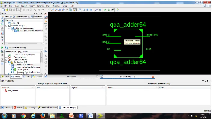
Fig.8 64-bit QCA adder
Figure 8 shows the internal RTL Schematic of novel 64-bit QCA Adder. As stated above, this can be obtained by using Xilinx.
Fig.9 basic modules used in adder
The figure 9 shows the technology schematic of novel 64-bit QCA adder obtained by using Xilinx. The operation of this can be explained with the help of above RTL schematic. As this is structure based design of Adder, some of its basic elementary blocks are given above in RTL view.
Fig.10 Simulation Result
The simulation output result is shown in figure 10 for 64 bit adder. The simulation result shows that the 64 bit QCA adder calculates the amount of delays and it reduces the number of cell count as well
In this paper we propose new design approach oriented to the implementation of full adders in QCA majority gates. We try to reduce the optimization parameters like complexity, area delay and power consumption.
we achieved better performance based on the above mentioned criteria, it is shown in the below table-1 And the output of both adders is simulated in Xilinx and model simulator and implement by using FPGA. Advantage:
An emerging computational nanotechnology called QCA has been a great help in learning more about the
primitive. Characterizing the three variable Boolean functions to a simplifying majority illustration using the Karnaugh maps (Kamp’s) is one of the easiest applications of majority gates.
The fundamental logic primitive gate is three inputs majority gate. Majority logic helps in the implementation of digital operations based on the principles of majority decisions. The logic elements a majority gate has an odd number of binary inputs and binary output. The output we get from majority gate is logical 1 when the majority of input is logic 1 and logical 0 when the majority of input is logic 0. We can implement any function or logical design as per requirement using a majority gates along with inverter.
Reference
[1] Stefania Perri cirsonello, and Giuseppe cocorullo,“Area-Delay Efficient Binary Adders in QCA” ,IEEE Trans. On very large scale integration systems, vol.22, no.5, 5May 2014
[2] H. Cho and E.E. Swartzlander, Jr., “Adder Designs and Analyses for Quantum-Dot Cellular Automata”, IEEE Trans. Nanotechnology, vol. 6, no. 3, pp. 374-383, May 2007
[3] H. Cho and E. E. Swartzlander, “Adder and multiplier design in quantum-dot cellular automata”, IEEE Trans. Comput., vol. 58, no. 6, pp. 721–727, Jun. 2009.
[4] S.Perri and P.Corsonello, “New methodology for the design of efficient binary addition in QCA”, IEEE Trans. Nanotechnol., vol. 11, no. 6, pp. 1192–1200, Nov. 2012.
[5] Kodam Latha,M.NandaMaharshi,“Design Of Adders Using QCA” ,International Journal of Advances in Engineering & Technology, Sept. 2013. ©IJAET ISSN: 22311963
[6] Bhuvaneswaran M,Shankar N.K.,“Efficient Design of MAC Hybrid Adder in Quantum-Dot Cellular Automata’’,International Journal of Advanced Research in Electrical, Electronics and Instrumentation EngineeringVol. 2, Issue 4, April 2013
[7] K.Walus, T. Dysart, G. Jullien, and R. Budiman, “QCADesigner: A rapid design and simulation tool for quantum-dot cellular automata,”IEEE Trans. Nanotechnol., vol. 3, no. 1, pp. 26–29, Jan. 2004
[8] R. Zhang, K.Walus, W. Wang, and G. Jullien, “ Performance comparison of quantum-dot cellular automata adders”, In IEEE International Symposium on Circuits and Systems, 2005, pages 2522–2526, 2005
[9 ] L. Lu, W. Liu, M. O’Neill, and E. E. Swartzlander, Jr., “QCA systolic array design,” IEEE Trans. Comput., vol. 62, no. 3, pp. 548–560, Mar.2013
[10] J. Huang and F. Lombardi, Design and Test of Digital Circuits by Quantum-Dot Cellular Automata. Norwood, MA, USA: Artech House, 2007.
[11] K Kong, Y. Shang, and R. Lu, “An optimized majority logic synthesis methology for quantum-dot cellular automata,”IEEE Trans. Nanotechnol., vol. 9, no. 2, pp. 170–183, Mar. 2010