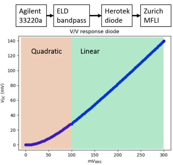
Diode based RF detector for STM
THESIS
submitted in partial fulfillment of the requirements for the degree of
MASTER OF SCIENCE
in PHYSICS
Author : L.K. Visscher
Student ID : 1284967
Supervisor : Dr. M.P. Allan
2ndcorrector : Prof.dr. J.M. van Ruitenbeek
Diode based RF detector for STM
L.K. Visscher
Huygens-Kamerlingh Onnes Laboratory, Leiden University P.O. Box 9500, 2300 RA Leiden, The Netherlands
February 21, 2018
Abstract
Currently the shot noise signal from the STM is measured with the Zurich MFLI lock in amplifier, which has measuring times on the order of
10 seconds. In this research we will build a RF diode detector. Starting out with the Herotek DZM020BB RF diode, we add additional components to increase its performance at measuring small signals. Then we compare its accuracy and measuring times with the Zurich MFLI. The detector had 1/f noise, which was eliminated with the ”tic toc” method.
Contents
1 Introduction 7
1.1 7
1.2 Scanning tunneling microscopy 7
1.3 Sources of noise in Scanning Tunneling Microscopy 9
1.4 The signal to be measured 11
1.5 Lock in amplifiers and diode detectors 12
1.5.1 Lock in amplifiers 12
1.5.2 Diode detectors 15
1.6 Outline of thesis 15
2 Creating a diode RF detector 19
2.1 Benchmarking the Herotek DZM020BB RF diode 19
2.2 Benchmarking the diode detector 20
3 Performance comparison of the diode detector with the Zurich
lock in 27
3.1 Sine signal 28
3.2 Noise signal 28
3.3 Measuring times and accuracy 30
4 Shift in the signal over time 33
4.1 Characterizing the shift 33
4.2 Heatsinks for the amplifiers 36
4.3 The tic toc method 39
5 Conclusion and recommendations 43
5.1 Conclusion 43
Chapter
1
Introduction
1.1
1.2
Scanning tunneling microscopy
In classical mechanics it is impossible for a particle to penetrate a potential barrier higher than its own energy. For example, a ball with insufficient initial energy will never roll over a hill but rolls back down instead. On the of scale of electrons, where particles behave according to the laws of quantum mechanics, this is not the case. Particles can end up on the other side of the barrier even if their energy is too low to penetrate it. This phe-nomenon is called ”quantum tunneling” and is important in a wide range of topics varying from nuclear fusion in stars [1] to mutations in DNA [2] and scanning tunneling microscopy [4].
Quantum tunneling can be modeled by the following one-dimensional potential given by Eqn. 1.1. In this case there is a potential barrier of height V0and depthd. A plot of this potential is shown in Fig. 1.1.
V(x) =
V0 for 0<x <d
0 elsewhere (1.1)
Transition rates can be calculated by solving the Schrodinger equation for this potential. For a derivation, see Griffiths [3].
T=
"
1+ V
2 0 4E(V0−E)
sinh2(κd)
#−1
(1.2)
ap-Figure 1.1:A plot of an idealized potential barrier.
proximate the transmission amplitude by:
T ≈16
E1−VE
0
V0 e
−2κd
(1.3)
The most important conclusion that can be drawn from Eqn. 1.3 is the fact that the transmission amplitude is exponentially dependent on the depth of the potential. Therefore the transmission amplitude is very sensitive for changes in this depth.
A technology that exploits this exponential relationship is called Scan-ning Tunneling Microscopy (STM) [4] and netted its inventors, Gerd Bin-nig and Heinrich Rohrer, the 1986 Nobel prize [5]. In STM experiments a metal tip is brought close to a sample surface and a bias voltage is ampli-fied. Even though there is no physical contact between the two materials current will still flow due to the quantum tunneling effect. In this context the height of the potential barrier is called the work functionφand is usu-ally on the order of 5 eV [6]. For this work function κ−1 will be on the order of 1 ˚A and therefore the STM is able to measure differences in dis-tance between tip and sample accurately down to fractions of an ˚A. When piezo-electrical motors are coupled to the set up to allow the tip to move around the surface a high resolution height map, a so called topograph, of the sample can be created.
1.3 Sources of noise in Scanning Tunneling Microscopy 9
Nowadays STMs are used to probe the microscopic physics of a di-verse range of phenomena. One example is research on superconducting materials, where their very high resolution has allowed the experimental verification of the theory of classical superconductors [16]. The precision of the STM can also be used in the other direction to deposit individual atoms on a sample [17].
1.3
Sources of noise in Scanning Tunneling
Mi-croscopy
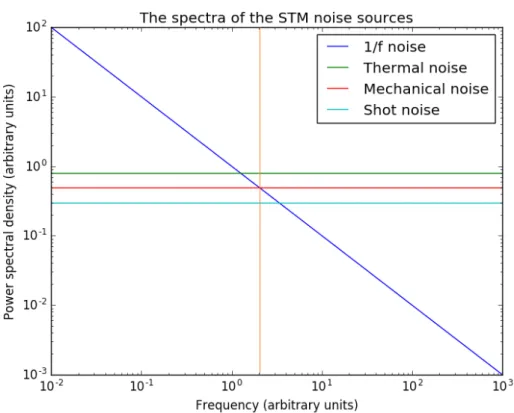
There is always an amount of noise present in STM, despite the efforts to minimize it as described in the previous section. Four types of noise are relevant for STM. The first one is the 1/f or pink noise. Its power spectrum is inversely proportional to the frequency. The universal mechanism that produces this types of noise remains elusive [7], but this type of noise is ubiquitous in widely varying systems such as networks of neurons, the financial markets and ecosystems [8]. In electronic systems it can be due to thermal fluctuations [9]. Its power spectral density is given by Eqn. 1.4 .
Spink = αI2
f (1.4)
In this equation I is the current and α is an empirical parameter that de-pends on temperature, applied voltage and the specific system. In STMs it typically varies between 10−3and 10−6[10].
The second type is Johnson-Nyquist or thermal noise and is due to the thermal excitation of charge carriers inside a conductor. Its power spectral densitySthermal does not vary with respect to the frequency and is given by Eqn. 1.5 [11].
S=4kBTR (1.5)
WherekB is Boltzmanns constant, Tis the temperature and Ris the resis-tance of the conductor.
The third type is mechanical noise, which like thermal noise, has a power spectral density independent of frequency.
root of the total DC current ¯I carried by carriers of charge q, as shown in Eqn. 1.6 [13].
Sshot =2q|I¯| (1.6)
when the temperature T is non-zero and an arbitrary voltageU is ap-plied on the tunnel junction, the power spectral density is given by Eqn. 1.7 [10].
Sshot =2qI¯coth
qRI¯ 2kBT
(1.7)
In the so called thermalization limit whereqU kBTEqn. 1.7 reduces to Eqn. 1.5 and the power spectral density will equal that of thermal noise., while ifqU kBTthe power spectral density is approximately given by Eqn. 1.6 and will be Poissonian.
In the low temperature limit the noise power will be linearly propor-tional to the charge transferred. This property allows the Fano factor Fto be calculated, which is defined in Eqn. 1.8.
F= Sshot
2e|I¯| (1.8)
Whereeis the elementary charge quantum.
The Fano factor is the ratio between the smallest unit of charge trans-ferred and the elementary charge quantum. In metals charge is carried by electrons and thus the Fano factor equals one, however in superconduc-tors, where the carriers are Cooper pairs, it is equal to two. Therefore the shot noise tells a lot about the material, but often it is orders of magnitude weaker than 1/f and thermal noise. To measure shot noise the experiment needs to be set up in such a way that shot noise is maximized and the other kinds of noise are minimized.
From Eqn. 1.4 and Eqn. 1.6 it can be derived thatSshot S1/f is true if
1.4 The signal to be measured 11
Figure 1.2: The spectral densities of the relevant noise sources for STM. On the x-axis is the frequency and on the y-axis the power spectral density. Both axes are on a logarithmic scale. When the frequency is lower than the critical frequency (the orange line), 1/f noise will dominate the noise.
1.4
The signal to be measured
The goal is to measure shot noise. To achieve this the Tamagotchi, the STM we are designing a detector for, has a double RLC tank combined with a high electron mobility transistor to amplify the signal. These were added to allow the measurement of shot noise, and its theoretical resonance fre-quency is around 2.8 MHz. This is high enough to filter out 1/f noise [14] [15].
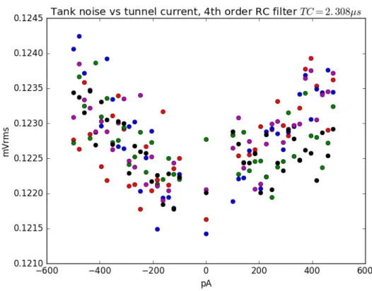
Fig. 1.3 is an noise vs current curve from this setup. The shot noise is linearly dependent on the current, while the thermal noise is independent. The difference in incoming root mean squared voltage between a current at the tip of 0 pA and 500 pA is about 3 % of the total signal. This means that the detector needs to have have a signal over noise ratio of at least 33. The RMS value of the signal is around 0.12 mV.
Figure 1.3: An noise vs current curve from Allan STM. On the x-axis is the cur-rent through the tunnel junction inpA, while on the y-axis gives the root mean squared voltage inmV of the signal detected at the lock in amplifier. Different colors correspond to different locations on the sample.
around 3 MHz with a width of 10 kHz.
1.5
Lock in amplifiers and diode detectors
1.5.1
Lock in amplifiers
1.5 Lock in amplifiers and diode detectors 13
sin(ωit)sin(ωrt) = 1
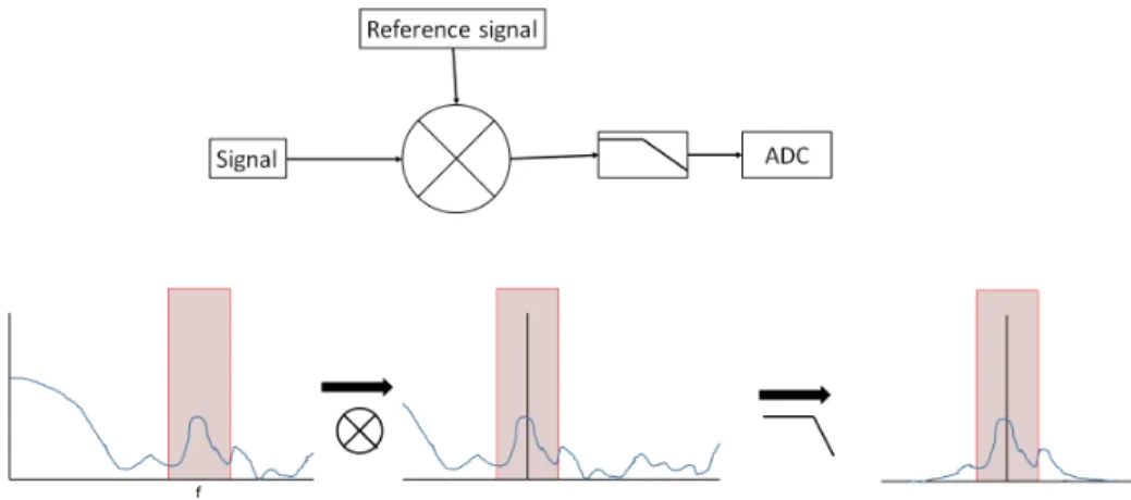
2[cos((ωi−ωr)t)−cos((ωi+ωr)t)] (1.9) Eqn. 1.9 shows that in general the result of this mixing will be two AC signals. However, the component of the signal with a frequency equal to that of reference signal will be shifted to DC. By placing a low-pass filter after the mixed signal, or by averaging the mixed signal over time, only the part of the spectrum close to the reference signal remains. This scheme is shown in Fig. 1.5. A Fourier transform of the mixed signal is called a zoomfftin Zurich MFLI terminology, because it is a zoom in on the part of the spectrum around the reference frequency.
Figure 1.5: Lock in operation. The upper picture is a schematic depiction of the lock in and the lower shows the effect of a lock in on the spectrum of the signal.A signal (red part of the spectra) is shifted to DC by mixing it with a reference signal (symbolized by the encircled ’x’). Then the higher frequencies are filtered out (symbolized by the l-shape) such that only the part of the spectrum close to the reference signal remains. The mixed filtered signal is then read by a analog digital converter (ADC).
This mixing to DC makes a lock in amplifier very capable in detecting narrow bandwidth signals buried in large bandwidth noise. In that case the signal to noise ratio can be improved by lowering the cut-off frequency or increasing the averaging time, which will filter out all the noise from frequencies outside the signal band.
1.6 Outline of thesis 15
increases the measuring time. A quicker way of measuring signal ampli-tudes are diode RF detectors.
1.5.2
Diode detectors
A diode is a semiconductor device that conducts current in one direction, the forward direction, and blocks it in the other, reverse, direction. This property is called rectification. A rectified AC signal has a nonzero av-erage voltage can convert AC to DC in this way. A rectifier can be built out of a single diode, but the DC output will have a significant ripple. By constructing more complicated rectifiers using multiple diodes and/or ca-pacitors this ripple can be mitigated. A demonstration of rectification is shown in Fig. 1.6. An ideal rectifier would output a constant DC signal proportional to the amplitude of the AC signal.
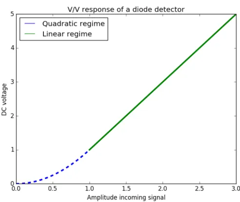
An ideal diode will have no resistance in the forward direction and infinite resistance in the reverse direction, but in a real diode current will only flow if the applied voltage (in the forward direction) is equal to or higher than the so called forward voltage. The forward resistance is also nonzero. This implies that when rectifying an AC signal the amplitude of the signal should be larger than the forward voltage of the diode to convert it into DC.
The relation between incoming AC amplitude and outgoing DC volt-age is called the V/V response of the diode. At low incoming voltvolt-ages the V/V response is quadratic, while at higher the response will be linear. An example of such a V/V curve is shown in Fig. 1.7.
The slope of the V/V curve is steepest in the linear regime. The goal of the detector is to measure small differences in signal amplitude, which translate into differences in DC voltage proportional to the slope. Thus the performance of the detector is best if the slope is maximal, which is in the linear regime. Therefore we want to measure in the linear regime of the diode.
1.6
Outline of thesis
Figure 1.6: The principle of diode rectification. The upper signal is AC. When passed through a diode the signal in the middle remains. Although the average voltage is nonzero, it is not a constant signal. The lower signal is a diode with a capacitor. The capacitor smooths out the signal, although there is still a ripple present.
1.6 Outline of thesis 17
Chapter
2
Creating a diode RF detector
In this chapter we will benchmark the Herotek DZM020BB RF diode by measuring its V/V response. Then we will add electrical components to improve its capacity in measuring low amplitude signals. The V/V re-sponses of those improved detectors and their performances at detecting low amplitude signals will also be measured.
2.1
Benchmarking the Herotek DZM020BB RF diode
It is best if the diode is measuring in its linear regime, as mentioned in the previous section. Therefore we characterize the V/V response of the diode to find the linear regime. The power of the STM signal is known, so finding the transition point between the quadratic and linear regime of the response will give the amount of amplification required in the detector.
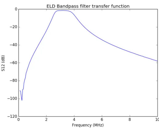
To measure the V/V response white noise was generated with the Ag-ilent 33120 function generator. This noise was filtered by an Elektronische Dienst (ELD) constructed band-pass filter to simulate the signal from the STM. The transfer function of this filter is shown in Fig. 2.1. Its bandwidth is larger than the PSD of the STM signal (shown in Fig. 1.4). The result-ing DC voltage was measured with Zurich MFLI. The input root mean squared voltages ranged from 0 mV to 300 mV. The sampling rate of the lock in was 100 Hz, the averaging time per data point was 1 s and the low pass filter was set to a cut-off frequency of 10.4 Hz.
Figure 2.1: The transfer function of the ELD constructed bandpass filter as mea-sured by the VNA. On the x-axis is the frequency inMHzand on the y-axis the S12 parameter indB. The −3 dB points are at2.7 MHz and3.8 MHz. Note that even in the frequency band there is a slight attenuation of−1.5 dB.
signal we want to measure has a root mean squared amplitude of around 120 µV, so an amplification of around 1000x is required.
2.2
Benchmarking the diode detector
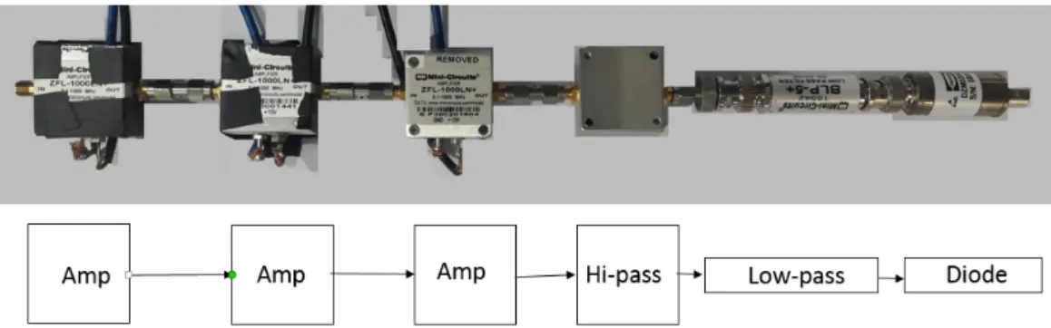
The 1000x amplication required is achieved by putting three Minicircuits ZFL-1000LN+ with a nominal gain of 23.5 dB before the diode. Amplifiers generate some white noise, therefore a low pass (Minicircuits BLP-5+) and high pass (Minicircuits ZFHP-1R2-S+) filter where placed behind the am-plifiers to filter out the parts of the noise spectrum outside the band of the signal. A photograph of the the detector is shown in Fig. 2.3.
2.2 Benchmarking the diode detector 21
Figure 2.2: The setup for measuring the V/V response of the diode (upper) and a plot of the V/V response of the diode (lower). On the x-axis is theVrms of the
incoming noise signal and on the y-axis is the DC output in volt. The red area is the quadratic regime, the green area the linear regime.
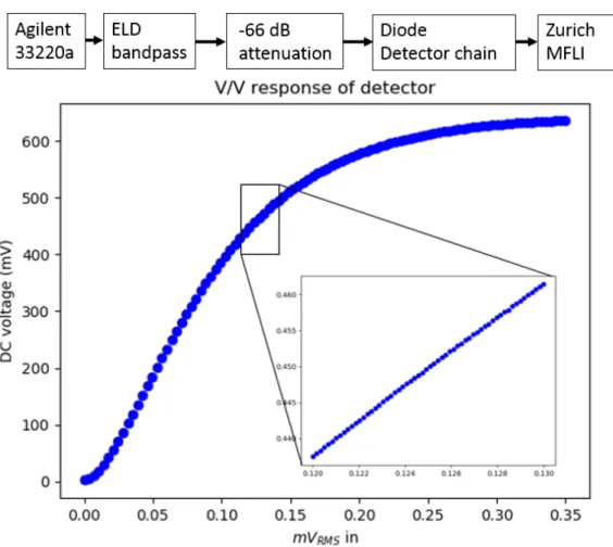
noise signals with a root mean squared voltage less than1.1 mV. This setup for measuring the V/V response and the V/V response itself is shown in Fig. 2.4. The attenuation allows generation of signals with a power of the same magnitude as that of the STM signal. The range of the input voltage for the detector ranged from 0 µV to 350 µV.
Figure 2.3:A photograph of the first version of the detector. The input is left, the output is right. From left to right: three Minicircuits ZFL-1000LN+ amplifiers, a Minicircuits BLP-5+ low pass filtes, a Minicircuits ZFHP-1R2-S+ high pass filter and the Herotek DZM020BB diode.
but these amplifiers are for small signals and their gain might diminish with higher voltage inputs.
The purpose of the complete detector setup is to measure small vari-ations in the signal and therefore a large slope in the detecting range is preferable, because the larger the slope, the larger the difference in DC output for small differences in input amplitude. To achieve this 6 dB atten-uation was placed between the first and second amplifier in the detector. The V/V response of this attenuated detector is shown in Fig. 2.5.
If attenuators are added between the first two amplifiers the curve be-comes linear at a root mean squared voltage in of 50 µV. The slope of the curve starts slightly decreasing at 200 µV, which is higher than the ampli-tude of the STM signal.
The attenuators were added to put the range of STM output in the range of maximum slope. However, the slope of the unattenuated de-tector (2397mVDC/mVRMS) is larger than that of the attenuated one (2316 mVDC/mVRMS) in the range of STM signal amplitudes (120 µV to 130 µV). This is due to the fact that the DC voltage of the attenuated detector is lower than that of the unattenuated one and thus the slope of the first is lower as well.
The detector will translate the root mean squared amplitude VRMS of an AC signal into a DC voltageVDC. In the measurement regime the V/V response can be fitted by a linear function as shown in Eqn. 2.1.
VDC =V0+αVRMS (2.1)
2.2 Benchmarking the diode detector 23
Figure 2.4: The measurement setup for the V/V response (upper) and a plot of the V/V response (lower) of the detector. On the x-axis of the graph is theVrms
of the incoming signal and on the y-axis is the measured DC voltage inmV. The inset figure is in the range of STM signal amplitudes. A linear fit for this part is also shown. The Zurich Lock In had a sampling rate of100 Hzand a sample time of1 s. Its 4th order low pass filter was set to10 Hz.
inverted to find the amplitude of the STM signal:
VRMS=
VDC−V0
α (2.2)
Figure 2.5: The measurement setup for the V/V response (upper) and a plot of the V/V response (lower) of the improved detector . On the x-axis of the graph is theVrms of the incoming signal and on the y-axis is the measured DC voltage in
mV. The inset figure is in the range of STM signal amplitudes. The Zurich Lock In had a sampling rate of100 Hzand a sample time of1 s. Its 4th order low pass filter was set to10 Hz.
2.2 Benchmarking the diode detector 25
Figure 2.6:A plot of the V/V curves of the unattenuated detector (upper) and the detector with 2 attenuators (lower). The data is represented by the blue dots and the fits by the red lines. On the x-axis is the incoming root mean squared voltage inmVand on the y-axis is the measured DC voltage inmV.
Chapter
3
Performance comparison of the
diode detector with the Zurich lock
in
Now that we have constructed a detector we will compare its performance with the lock in. The accuracy of the MFLI and the diode detector chain in measuring signal amplitudes will be compared by measuring the res-olution R for a 3 MHz pure sine signal and for the filtered noise signal from the previous section. Both signals will be attenuated by−66 dB us-ing Minicircuits VAT series attenuators to simulate the low amplitudes of the STM signal.
The signal from the STM has a narrower bandwidth but is not a pure sine signal and is phase incoherent. The STM signal is therefore in be-tween the wide bandwith filtered noise or a pure 3 MHz sine signal. In this test the input root mean squared voltage at the lock in or diode de-tector will vary from 125.5 µV to 128.5 µV in steps of 0.1 µV. The setup for these comparisons is shown in Fig. 3.1.
Figure 3.1: The scheme for comparing the performance of the lock in and the diode detector chain. The function generator will either output white noise or a3 MHzsine. The output then passes through the ELD bandpass filter (see Fig. 2.1) and−66 dBMinicircuits VAT attenuators. The detector is just the MFLI when quantifying the performance of the MFLI, or the diode detector chain followed by the MFLI measuring the output DC.
3.1
Sine signal
The sine signal was generated by the Agilent 33120 function generator and was attenuated by 66 dB and the ELD bandpass filter (see Fig. 2.1) to put it in the same voltage range as the typical signal coming from the STM. The results for the Lock In and the diode detector are shown in Fig. 3.2.
We find values for Rof 0.0193 µV for the lock in and 0.0226 µV for the detector. The lock in is more precise in this case. Note that the measured VRMS and the input are not the same for the lock in. This is probably caused by the attenuators not attenuating precisely 66 dB and the error in the signal generated by the function generator. The goal is to compare the precision of the diode detector with that of the lock in and both will still measure the same signal, so the comparison is still valid.
3.2
Noise signal
3.2 Noise signal 29
Figure 3.2:The VV curves of the lock in (upper) and diode detector (lower) for the
3 MHzsignal. On the x-axis the root mean squared amplitude of the signal in mil-livolts and on the y-axis is the root mean squared voltage in milmil-livolts measured by the lock in and DC voltage in millivolts respectively. The blue dots represent the measured amplitude and the red lines correspond to the linear fit.
Fig. 2.1). The results for the lock in and the diode detector are shown in Fig. 3.3. The measuring time was equal to 10 seconds (60 spectra per point for the lock in).
Figure 3.3:The VV curves of the lock in (upper) and diode detector (lower) for the filtered noise signal. On the x-axis the root mean squared amplitude of the signal in millivolts and on the y-axis is the root mean squared voltage in millivolts as measured by the lock In and DC voltage in millivolts respectively. The blue dots represent the measured amplitude and the red lines correspond to the linear fit.
rates than 107.1 kHz were also tried, but those resulted in errors when transferring data from the lock in to the measurement PC.
3.3
Measuring times and accuracy
3.3 Measuring times and accuracy 31
1 to 10 seconds in steps of 1 second) and the sampling times for the diode detector were 1 s to 10 s increasing in steps of 1 s. The results are shown in Fig. 3.4.
(a)Noise signal (b)3 MHzsignal
Figure 3.4: The resolution in µV(y-axis) plotted against the sampling time per point in seconds (x-axis) for the noise signal (left) and the 3 MHzsignal (right). The blue dots correspond to the diode and the red dots to the Lock In.
In case of a noisy signal the resolution for the diode equals around 0.02 µV for all sampling times except for a small peak at 2.5 s of 0.04 µV. The resolution of the Lock In improves with higher sampling times, from 0.16 µV at 1 s to 0.06 µV at 12 s.
With the sine signal the resolution for both the Lock In and the diode detector remains constant for different sampling times at 0.019 µV with exception of a few peaks. We suspect that these peaks are due to external interference. For example the setup is very sensitive to movement and these peaks might be due to someone touching the setup while doing the measurements.
Chapter
4
Shift in the signal over time
In the previous chapter we showed that the resolution of the diode detec-tor is better than that of the lock in. With Eqn. 2.2 the amplitude at the detector of the incoming signal can be calculated. It seemed the detector could be added to the STM setup. However, when we fitted the parame-ters in Eqn. 2.2 from a single curve and later used those to calculate the signal amplitudes we noticed that after a while the measured amplitudes were not correct anymore. There is a shift in the DC signal over time.
In this chapter we will first characterize this shift. After the shift is characterized two methods of mitigating its effect will be tested: heatsinks for the amplifiers and the ”tic toc” method.
4.1
Characterizing the shift
To understand why this happens several V/V curves were measured. The input signal was filtered noise with root mean squared amplitudes ranging from 125.5 µV to 128.5 µV subdivided into 30 points. These curves are shown in Fig. 4.1.
The fitted parameters of the curve vary over time. In Fig. ?? it can be seen that the slope increases, starting at 0.0014 VDC
µVRMS at 5 minutes to 0.0022 VDC
µVRMS at 50 minutes.
Figure 4.1:V/V curves taken at different times. On the x-axis is the amplitude of the signal inµVand on the y-axis is the DC voltage in V. The time of each curve is indicated in the lower left corner and is the time when the measurement of the curve was finished. The zero time was the time of switching on the power supply of the amplifiers.
The previous measurements were taken over the course of less than an hour and the rate of change for both the slope and the offset decreases with time. Therefore we want to take a longer measurement to characterize the changing behavior of the diode detector.
To characterize the shift in DC voltage over time V/V responses of the diode detector, the amplifiers and the diode on its own were measured over 8 hours. The type of signal was a 3 MHz sine instead of the noisy signal, because the am and the signal amplitude range was from 125.5 µV to 128.5 µV subdivided into 30 points.
4.1 Characterizing the shift 35
own. For just the diode the range was 125.5 mV to 128.5 mV subdivided into 30 points. Note that this amplitude is in the linear regime of the V/V curve. The sampling time of each point was 10 s and the sample rate was 100 Hz for DC measurements. For the amplifier measurements 60 spec-tra were measured per point. The amplitude range was the same as the completed detector measurement. The setups are shown in Fig. 4.2.
Figure 4.2:The setups for measuring the shift in output over time for the complete detector (upper), amplifiers (middle) and the diode (lower). The same equipment was used as in the previous sections.
To compare the shift in measured amplitude for the different compo-nents of the detectors we define the relative deviation:
VR = V−V¯
¯
V ∗100% (4.1)
The relative deviation of the output is shown in 4.3.
There is a steep decrease inVRfor the complete detector over the first hour, from 4.5% to 0.5%. From 1 hour to 6 hours it slowly decreases, from 0.5% to -0.5%, after which it starts increasing again to -0.2% at 8 hours.
TheVRof the diode increases from -1.5% to around 0% in the first hour, and then starts fluctuating around 0, with a root mean square amplitude of 0.14%.
With the amplifierVR decreases from 2.4% at the start to -0.1% at one hour. Then it slowly increases to 0.1% at 8 hours.
We believe the sharp decrease and increase for the amplifier respec-tively diode to be caused by a warming up of the components. After one hour the device reaches equilibrium temperature, and while there is still some shift it is not as dramatic as in the first hour. These shifts might be caused by changes in ambient temperature which will also shift the equi-librium temperatures slightly. The effect of heating on the V/V responses of the components can also be seen in Fig. 4.4.
Figure 4.3:The shift in output voltage over time. On the x-axis the time in hours, on the y-axis the relative deviation from the mean VR = V−V¯V¯. The blue, green
and red lines correspond to the complete detector, the diode on its own and the amplifiers on their own respectively.
the detector will be at its equilibrium temperature when measuring STM signals. The Fourier transform and fit are shown in Fig. 4.5.
The fit has an exponentα of -0.98, which is approximately equal to -1. This means that the shift of the signal over time is due to 1/f noise. Since the signal is DC this noise can not be eliminated by a low pass filter. There-fore we will try two methods of eliminating it, heatsinks for the amplifiers and the ”tic toc” method.
4.2
Heatsinks for the amplifiers
de-4.2 Heatsinks for the amplifiers 37
(a) Heating of the amplifier over time.
(b)Heating of the diode over time.
Figure 4.4: The effect of heating on the amplifiers (left) and diode (right). The components were heated with a heatgun starting around the300 smark. The
Figure 4.5:The Fourier transform of the complete detector signal (blue dots) and the fit (red line).
Figure 4.6:The shift in output voltage for the detector with heatsinks on the am-plifiers (green line) compared to that of the original detector (blue line). On the x-axis is the time in hours and on the y-axis the relative deviation from the mean.
There is still the initial drop in voltage for both the original detector and the detector with heatsinks. For the the original detector this drop is from 4.5% to 0.5% and for the detector with heatsinks it is from 2.5% to 0.0%. Thus this initial drop is smaller when heatsinks are installed. This is because the heatsinks decrease the equilibrium temperature, and thus the difference between initial temperature and heated up temperature is smaller for the detector with heatsinks. This also decreases the size of the drop.
4.3 The tic toc method 39
4.3
The tic toc method
Although the heatsinks improve performance the shift in DC voltage is still present. To reduce the effect of this shift we will introduce the ”tic toc” method, which is similar to the ”tic toc” method devised by Lafe Spietz in his PhD thesis [18].
The V/V response of the diode detector is linear in the signal ampli-tude range of 125.5 µV to 128.5 µV and given by Eqn. 2.1. This can be rewritten as:
VDC =α(t) (VRMS−V0) +Voffset(t) (4.2) Here V0 is a reference input amplitude. α(t) is the slope of the curve andVoffset(t)is an offset. To find the root mean squared amplitude of the signal we take the inverse of this function:
VRMS =
VDC−Voffset(t)
α(t) +V0 (4.3)
We expect bothαandVoffsetto be time dependent. To test this we mea-sured these parameters for 144 V/V curves taken over 12 hours, as shown in Fig. 4.7.
The difference between lowest and highest value of the slope is around 0.12 mVDC/µVRMS. The range is 3 µV wide, which means a variation of around 0.36 mV in DC voltage from the detector. The difference between lowest and highest value of the offset equals 5 mV. Thus the largest part of the shift in the signal is due to the shift in the offset. This variation in time can also be characterized by its Fourier transform. This is shown in Fig.??.
There seems to be no clear trend in the Fourier transform of the slopes. This is not the case with the offsets, however. The Fourier transform of the offset can be fitted to the function xab. This results in a = 3.4·1)6and b =0.98. This shows that the noise in the offset is 1/f noise. But there is a way to correct for this.
WhenVRMS =V0the output DC voltage will equalVoffset(t). Therefore the offset can be recalibrated regularly and we can mitigate the effect of its shift. We call this the ”tictoc” method, as it is similar to the ”tictoc” method devised by Lafe Spietz in his PhD thesis [18].
Figure 4.7: The slopes (upper) and offsets (lower) over time. On the x-axis is the time in minutes and on the y-axis is the slope inmVDC/µVRMS respectively the
offset inmVDC.
(at VRMS = 125.5µV) as the calibration point. The slope of the fit is de-termined from the first V/V curve from Fig. 4.1. In this way we can plot the resolution over time. This can be compared to the resolution over time without tictoc from the same datasets. The results are shown in Fig. 4.9.
With tic toc the resolution never becomes higher than 0.06 µV for both data sets. The mean of the resolution equals 0.3 µV while without it in-creases to 2 µV for the data from Fig. ??. For the second data set the reso-lution is maximally 0.3 µV without tic toc.
4.3 The tic toc method 41
Chapter
5
Conclusion and recommendations
5.1
Conclusion
The diode on its own is not sensitive enough to measure signals with am-plitudes on the order of 100 µV. When amplifiers are added before the diode in the detector chain the detector can detect these signals. The mea-suring time in this case is 1 s.
The V/V response of the detector changes with time due to among other things the temperature. However, this problem can be mitigated by using the tictoc method.
The diode detector can detect signals in the range of 125 µV to 129 µV root mean squared amplitude with a resolution of 0.06 µV with a measur-ing time of 1 second. This should be sufficient to do measurements of the STM signal, provided there is a way of regularly calibrating the detector.
5.2
Recommendations
The performance of the detector is not tested in other ranges than 125 µV to 129 µV. Additionally the frequency of calibrating for the tic toc method was not optimized. A follow up research could explore these topics.
5.3
Acknowledgements
Bibliography
[1] Newton J.R. et al. (2007)Gamow peak in thermonuclear reactions at high temperatures.Physics Review C 75 045801.
[2] Lowdin P-E (1963)Proton tunneling in DNA and its Biological Implica-tions.Reviews of Modern Physics Vol. 35–3 pp. 724–731.
[3] Griffiths D. (1995) Introduction to quantum mechanics Upper Saddle River, New Jersey, Prentice Hall Inc.
[4] Binnig G. & Rohrer H. (1983)Scanning Tunneling Microscopy. Surface Science Vol. 126 pp. 236–244.
[5] The Royal Swedish Academy (1986) The Nobel Prize in Physics 1986 [press release]. Retrieved from https://www.nobelprize.org/
nobel_prizes/physics/laureates/1986/press.html.
[6] Chen C.J. (1993)Introduction to Scanning Tunneling Microscopy.Oxford: Oxford University Press.
[7] Weissman M.B. (1988)1/f noise and other slow, nonexponential kinetics in condensed matter.Rev. Mod. Phys. Vol. 60, pp. 537.
[8] Bosman G. (2001) Noise in Physical Systems and 1/f Fluctuations. Pro-ceedings of the 16th International Conference.
[9] Hooge F.N., Kleinpenning T.G.M. and Vandamme L.K.J. (1981) Ex-perimental studies on 1/f noiseReports on Progress in Physics Vol. 44, 1981
Review Vol. 32 pp. 97–109.
[12] Schottky W. (1918)Uber spontane Stromschwankungen in verschiedenen Elektrizitatsleitern.Annalen der Physik Vol. 326–23 pp. 541–567.
[13] Blanter Ya. M. & Buttiker M. (2000)Shot noise in mesoscopic conductors. Physics Reports Vol. 336 pp. 1–166
[14] Benschop T. (2016) Developing a high frequency current amplifier for Scanning Tunnelling Microscopy.Bachelor thesis
[15] Leemker M. (2017)High frequency amplifier for the detection of shot noise in Scanning Tunneling MicroscopyBachelor thesis
[16] Fischer Ø. (2007) Scanning tunneling spectroscopy of high-temperature superconductorsReviews of Modern Physics Vol. 79–353
[17] Stroscio J. & Celotta R. (2004)Controlling the Dynamics of a Single Atom in Lateral Atom ManipulationScience Vol. 306–5694