An Analytic Model for Kink Effect in I-V Characteristics of
Single Electron Transistors
A. Shahhoseini*, K. Saghafi**, M. K. Moravvej-Farshi*** and R. Faez****
Abstract: In this paper, we have investigated the effects of asymmetry in the source and
drain capacitance of metallic island single electron transistors. By comparing the source and drain Fermi levels, in the ground and source referenced biasing configurations, with the island’s discrete charging energy levels for various gate voltages, we have derived a set of closed form equations for the device threshold voltage. Extending our technique, for the first time, we have also modeled the “kink effect” appearing in the device ID-VDS characteristic, next to the threshold voltage. To demonstrate how accurate the calculated values of the threshold and kink voltages obtained from the analytically derived formulas are, next, we have used the master equation based on the orthodox theory to simulate the device parameters, numerically. Comparisons of the numerical results, obtained from both techniques, have demonstrated the tolerances in our analytical calculations, for the worst case, are less than 1%.
Keywords: Single Electron Transistor, Coulomb Blockade, Master Equation, Kink Effect.
1 Introduction1
Breathtaking progress in modern CMOS technologies has pushed the device dimensions toward a certain limit, causing complications in device scalability and power consumption issues. A promising alternative device that could overwhelm such problems is the single electron transistor (SET) [1-3]. SETs operation is based on Coulomb blockade and single-electron tunneling processes. Although, at first glance, it might seem favorable to have a symmetric single electron transistor (SSET), experimental and theoretical studies of SETs with asymmetric source/drain junction resistances and capacitances have drawn much attention [4-6]. While Inokawa et al [4] and Mahapatra et al [5] have modeled asymmetric single electron transistors (ASETs) analytically; Doiron et al [6] have studied the electron
Iranian Journal of Electrical & Electronic Engineering, 2009. Paper first received 13 April 2009 and in revised form 12 Sep. 2009. * The Author is with the Department of Electrical Engineering, Sciences & Research Branch, Islamic Azad University, Tehran 1477893855, Iran.
E-mail: [email protected]
** The Author is with the Department of Electrical Engineering, Shahed University, P. O. Box 18155-159, Tehran 3319118651, Iran. E-mail: [email protected]
*** The Author is with the Advanced Device Simulation Lab (ADSL), Department of Electrical and Computer Engineering, Tarbiat Modares University, P. O. box 14115-143, Tehran 1411713116, Iran. E-mail: [email protected]
**** The Author is with the Department of Electrical Engineering, Sharif University of Technology, Tehran, Iran.
E-mail: [email protected]
transport in an ASET coupled to an oscillator. Recent developments have shown the advantages of an ASET in designing a quantum computer [7] and also fabricating a quantum amplifier [8]. Furthermore, Mizugaki et al. in their most recent report [9] have presented a technique for optimizing such transistors. Using the Coulomb Blockade Stability Diagram, they have derived a relation for the difference between positive and negative threshold voltages. Our focus, in this paper, ASETs, whose asymmetry is due to inequality in S/D capacitances, and we call them CASETs.
Rest of the paper is organized as follows. After presenting the modeling backgrounds in Section 2, we demonstrate a graphical scheme to compare source/drain Fermi levels (SFL/DFL) with the island charging energy levels (CEL), in Section 3, where we present closed form formulas for both SSETs and CASETs threshold voltages. The graphs used in this scheme enable us to demonstrate conditions at which an electron can tunnel into (out of) the island. In Section 4, we present an analytic method for analyzing the “kink effect” in both SSETs’ and CASETs’ I-V characteristics. We also demonstrate that by applying a suitable gate voltage, the kink effect disappears. In Section 5, we compare the numerical results obtained for various CASETs with those obtained from closed form formulas. Finally, we close this paper by conclusion, in Section 6.
2 Modeling Backgrounds
A SET consists of a conductive island surrounded by two tunnel junctions, known as source (S) and drain (D). These tunneling junctions contribute resistances, RS/D, and capacitances CS/D, to the device. In the theory of single electron tunneling, the tunneling resistance of the island should be larger than the quantum resistance, RQ=25.8 kΩ. This condition ensures a reasonably long lifetime of an excess electron on an island [3]. Therefore, we can ignore the effect of electrons lifetime in the island. The island is coupled to the gate voltage, VG, via a gate capacitance, CG. Therefore, the total capacitance of the island is CΣ=CS+CD+CG. The models that we have used are based on the orthodox theory, in which the discrete charging energy levels inside the island are considered and quantum size effects may be ignored [10]. On the other hand, when the metallic island size is about 10nm, the alteration of EF is negligible in compare to electroestatic energy e2/2C
Σ
[11]. We have used the Master equations in steady state to obtain device current-voltage, ID-VDS, characteristics [12]. Solving such equations, we have calculated the probability, P(n), of finding a state in which the nth electron either enters or exits the island.
The existing biasing configurations for SETs are either the ground referenced (GR) or the source referenced (SR) models. Schematics of such biasing configurations are illustrated in Fig. 1. For the GR-SET, as shown in Fig. 1(a), it is assumed VD=−VS=(VD−VS)/2≡VDS/2, with VD and VS as the drain and source biases, respectively. Although the simulation results obtained for such a biasing configuration are simpler, the SR model of Fig. 1(b) is more suitable for circuit level simulations.
In general, we assume that in equilibrium the island contains n electrons, with electrostatic energy, Ech(n), and the nth charging energy level, CELn, are expressed as [3]:
2
( ) (= − + ) 2 Σ
ch ext
E n ne Q C (1)
and
( 1) ( )
( 1/ 2) Σ
= + −
= ⎡⎣ + − ⎤⎦
n ch ch
ext
CEL E n E n
e n e Q C (2)
respectively, where e is the electronic charge and
= + +
ext S S D D G G
Q C V C V C V (3a)
is the charge induced on the island by external voltages. For the ground-referenced (GR) and source-referenced (SR) models, (3a) reduces to,
(
)
(GR) 2
2
Δ
= − +
≡ +
ext D S DS G G
DS G G
Q C C V C V
CV C V (3b)
(SR)= +
ext D DS G GS
Q C V C V (3c)
(a)
(b)
Fig. 1 Biasing configurations for a SET as (a) Ground
referenced (GR); (b) Source referenced (SR)
From (2), one can see that the neighboring CELs, for all SETs in general, are equally spaced; i.e.
2 1 Σ, −
− =
n n
CEL CEL e C (4)
which corresponds to the charging energy of an electron. Furthermore, a change of ΔVG=±e/CG, in the gate voltage results in a change of ΔQext=±e in (3a)-(3c). This, in turn, is equivalent to lowering or raising CELn, in (2), by one level; i.e.
2
1
( / ) ( )
( ).
Σ
± =
≡ m
m
n G G n G
n G
CEL V e C CEL V e C
CEL V (5)
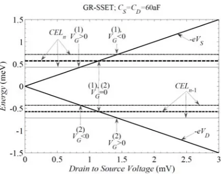
For a SSET, the term ΔC≡(CD−CS) vanishes and (3b) reduces to Qext(GR)=CGVG, while (3c) is unaffected. Hence, for a GR-SSET, CELn is independent of VDS. Whereas, for a SR-SSET Qext and hence CELn vary linearly with VDS. Furthermore, as one can see from (2) and (3), CELs of an island in a SET are independent of RS/D. On the other hand, for a CASET in which ΔC≠0, one can see the linear dependence of CELn, on VDS, regardless of the biasing configuration.
3 Tunneling Conditions and Threshold Voltages
When a SET is biased by applying external voltages an electron may tunnel in or out of its island. Fundamental conditions for electron to tunnel across a tunneling junction depend upon the relative position of
SFL and DFL with respect to CEL). By definition, the threshold voltage, VTH, in a SET, is the minimum VDS for which such condition is satisfied.
Consider an island, subject to VG=0, containing n electrons at equilibrium. In order to enable (n+1)th electron tunnels into the island, from either source or drain, an appropriate biasing condition is needed to increase the corresponding Fermi level beyond the island CELn. On the other hand, to enable nth electron to tunnel from island out to either source or drain regions, an appropriate biasing condition is required to lower the corresponding Fermi level below CELn−1. A sufficient increase in VDS, increases the separation between SFL and DFL, surrounding one or more CELs in between. This enables electrons to tunnel into and out of the island, increasing the drain current, ID, as a result.
Now, we use a graphical scheme to demonstrate the conditions by which an electron may tunnel into/out of the island, for both SSETs and CASETs, in more details. Fig. 2 illustrates VDS dependence of the SFL, DFL, and the island CELs of a SSET with CS=CD=60aF, CG=20aF, and RS=RD=160kΩ, biased in GR configuration. These variations are associated with tunneling of the first electron from the source to the island (S/I) or from the island to the drain (I/D). To avoid complications, in drawing such figures, we have assumed an offset in, by setting n=0.
As shown in Fig. 2, due to symmetry that exists in the relative positions of CELn and CELn−1 with respect to SFL an DFLof the GR-SSET biased at VG=0, they intersect SFL and DFL for the same VDS. As shown in Fig. 2, for VG=0, VDS1=VDS2. On the other hand, in a GR-CASET in general, the threshold voltage required for an electron to tunnel across S/I, VDS1-GR, can be obtained from CELn=−eVS=eVDS/2,
1 GR
2 (2 1)
Σ Δ −
− + +
=
+ G G DS
C V e n
V
C C (6)
while the threshold voltage, required for an electron to tunnel across I/D, VDS2-GR, for the same device, can be obtained from CELn−1=−eVD=−eVDS/2,
2 GR
2 (2 1)
Σ Δ −
− −
=
− G G DS
C V e n
V
C C (7)
The general condition for simultaneous tunneling across S/I and I/D junction is obtained by equating (6) and (7), which results in,
(
)
0 GR− = −Δ 2 Σ
G
G
e
V n C C
C (8)
otherwise, the threshold voltage is determined by minimum of absolute values of Eqs. (6) and (7),
Fig. 2 VDS dependence of SFL, DFL, CELn, and CELn−1 a GR-SSET with CS=CD=60aF, CG=20aF, and RS=RD=160kΩ, illustrating the junctions tunneling conditions
(
)
(
)
GR-CASET
2 GR 0 GR
1 GR 0 GR
for 1 2
for 1 2
−
− −
− −
=
⎧ − < ≤
⎪ ⎨
≤ < +
⎪⎩
TH
DS G G G
DS G G G
V
V e n C V V
V V V e n C
(9a)
As one can realize from Eqs. (6) and (7), only for gate voltages satisfying the condition (n−1/2)e/CG<VG< (n+1/2)e/CG, both VDS1-GR and VDS2-GR and hence (9a) become positive. Note that, 0<|ΔC|/CΣ<1. For our
examples, the defined region is −4mV<VG<4mV.
For a GR-SSET, however, ΔC=0 and the denominators of both (6) and (7) become equal to CΣ,
and hence, the simultaneous tunneling across the two neighboring junctions of a SSET sustains only for VG0-GRSSET=en/CG, and (9a) reduces to
(
)
(
)
GR-SSET
DS2 GR
DS1 GR
( ) for 1 2
( ) for 1 2
− − −
= =
⎧ − < ≤
⎪
⎨ =
≤ < +
⎪⎩
TH
S D G G G
S D G G G
V
V C C e n C V en C
V C C en C V e n C
(9b)
Fig. 3 illustrates the threshold conditions for electron tunneling across S/I and I/D junctions for a SR-SSET with the same capacitances and resistances as those of Fig. 2.
As seen from this figure, for VG=0, VDS1≠VDS2. To find the condition for simultaneous tunneling across S/I and I/D junctions, for the SR biasing configuration, one should set CELn=0 and CELn−1=−eVDS. In general, this leads us to
(
)
1 SR
1 2
−
− + +
= G GS
DS
D
C V e n
V
C (10)
and
Fig. 3 VDS dependence of SFL, DFL, CELn, and CELn−1 a SR-SSET with CS=CD=60 aF, CG=20 aF, and RS=RD=160 kΩ, illustrating the junctions tunneling conditions
(
)
2 SR
1 2
Σ −
− −
=
− G GS DS
D
C V e n
V
C C (11)
The conditions for which both (10) and (11) become positive are exactly the same as those for (6) and (7). By equating (10) and (11), the gate bias condition for simultaneous tunneling across two neighboring junctions of a SR-CASET becomes
(
)
0 SR− = +1 2− Σ
GS D
G
e
V n C C
C (12)
In general, the threshold voltage for a SR-CASET is determined by the minimum of the absolute values of (10) and (11),
(
)
(
)
SR-CASET
2 SR 0 SR
1 SR 0 SR
for 1 2
for 1 2
−
− −
− −
=
⎧ − < ≤
⎪ ⎨
≤ < +
⎪⎩
TH
DS G G GS
DS GS G G
V
V e n C V V
V V V e n C
(13)
Note that 0<CD/CΣ<1.
For a SR-SSET, however, the threshold voltage is simply obtained by substituting CD=CS (or CΣ=2CD+CG) into (10)-(13). As indicated in the example illustrated in Fig. 3, for this particular case, simultaneous tunneling occurs at VGS0≈0.571 mV for which VDS1=VDS2≈1.143 mV.
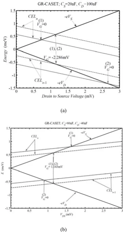
Fig. 4 illustrates two graphical examples for tunneling conditions in GR-CASETs. All physical parameters, used in these two examples, are the same as those used in Fig. 2, except for CS and CD.
The charging energy levels, for each example, are drawn for VG=0 and another one, obtained from (8), which satisfies the condition for simultaneous tunneling across S/I and I/D. That is, VG=−2.286 mV, for the
GR-CASET with CS=20 aF and CD=100 aF, as illustrated in Fig. 4(a), and VG=1.143 mV, for GR-CASET of Fig. 4(b) with CS=80 aF and CD=40 aF. As one can observe, by comparing these two examples, for an asymmetry with CD>CS the slope of the CELs are negative, while for the case with CD>CS the slopes become positive. Hence, for VG biases that do not satisfy (8), the tunneling sequence across two neighboring junctions, for these two cases, alters.
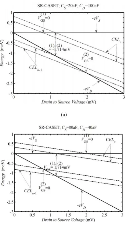
Fig. 5 illustrates the tunneling conditions for the two SR-CASETs with physical parameters same as those of Fig. 4. CELs, for each example in this case, are drawn for VGS=0 and the one (12). That is, VGS1=−1.714 mV, for the SR-CASET with CS=20 aF and CD=100 aF, as illustrated in Fig. 5(a), and VGS1=+1.714 mV, for SR-CASET of Fig. 5(b) with CS=80 aF and CD=40 aF.
(a)
(b)
Fig. 4 VDS dependence of the SFL, DFL, CELn, and CELn−1 of a GR-CASET with (a) CD=100 aF and CS=20 aF, for VG=0 and −2.286 mV, and (b) CD=40 aF and CS=80 aF, for VG=0 and +1.143 mV. RS=RD=160 kΩ, CG=20 aF, for both CASETs
(a)
(b)
Fig. 5 VDS dependence of SFL, DFL, CELn, and CELn−1 of a SR-CASET with (a) CD=100 aF and CS=20 aF, for VGS=0 and −1.714 mV, and (b) CD=40 aF and CS=80 aF, for VGS=0 and +1.714 mV. RS=RD=160 kΩ, CG=20 aF, for both CASETs
Although, as illustrated in this figure, the charging energy levels slopes, for both cases, are negative, those of the SR-CASET with CS>CD are more positive than the corresponding slopes for SR-CASET with CS>CD. Hence the threshold condition for S/I tunneling, in the former device, prevails before that for the tunneling across I/D junction, contrary to the tunneling sequence in the latter device.
4 Kink Effect
As VDS increases beyond VTH, large enough to bring the second charging energy level between the SFL and DFL, one may see a “kink” in the device ID-VDS characteristics of SETs, biased in both GR and SR. Appearance of such an effect not only depends on the biasing conditions but also on the sign of ΔC and size of CD/CΣ for GR and SR configurations, respectively.
Although VTHis found from the minimum of either (6) and (7) or (10) and (11), their maximum might not be the kink voltage, Vkink. In fact, to find the VDSfor which the second charging energy level enters between the SFL and DFL, we need to compare the source to drain voltages found from equating CELn and CELn+1 with SFL=−eVS and CELn−1 and CELn−2 with DFL=−eVD.
For a GR-CASET, CELn+1=−eVS=eVDS/2 results in
3 GR
2 (2 3)
Σ Δ −
− + +
=
+ G G DS
C V e n
V
C C (14)
and CELn−2=−eVD=−eVDS/2 gives
4 GR
2 (2 3)
Σ Δ −
− −
=
− G G DS
C V e n
V
C C (15)
Note that for (n−1/2)e/CG<VG<(n+1/2)e/CG, Eqs. (14) and (15) are both positive. For gate biases satisfying the simultaneous tunneling conditions, defined in Eq. (8), Vkink is determined from the minimum of Eqs. (14) and (15). Otherwise, Vkink is the second lowest VDS among Eqs. (6), (7), (14), and (15). Comparing these four equations, at the first glance, one realizes that VDS3-GR>VDS1-GR and, VDS4-GR>VDS2-GR, for any arbitrary condition. Since we have already compared VDS1-GR andVDS1-GR, to find the Vkink and its corresponding VGrange, we need to compare VDS3 with VDS2 and VDS4 with VDS1. For example, when VDS2-GR >VDS3-GR then VTH=VDS1−GR and Vkink=VDS3-GR, while for VDS1-GR>VDS4-GR, VTH=VDS2−GR and Vkink=VDS4-GR. For a more general analysis, we should consider two cases depending on the sign of ΔC.
Case 1 (ΔC>0): In this case, Vkink is found to be
(
)
(
)
GR-CASET
1 GR 0 GR
3 GR 0 GR
2 GR 0 GR 1 GR
3 GR 1 GR
for 1 2
for
for 0
for
for 1 2
Δ −
− −
− −
− − −
− −
=
⎧ − < <
⎪
= ⎪
>
⎨ < <
⎪
⎪ < < +
⎩
kink
DS G G G
DS G G
DS G G G
DS G G G
V
V e n C V V
V V V
C
V V V V
V V V e n C
(16)
where
(
)
1 GR− = +1 2−Δ Σ for Δ >0
G
G
e
V n C C C
C (17)
Case 2 (ΔC<0): In this case, Vkink is found to be
(
)
(
)
GR-CASET
4 GR 2 GR
1 GR 2 GR 0 GR
4 GR 0 GR
2 GR 0 GR
for 1 2 for
for 0
for
for 1 2
Δ −
− −
− − −
− −
− −
=
⎧ − < <
⎪ < <
⎪
<
⎨ =
⎪
⎪ < < +
⎩
kink
DS G G G
DS G G G
DS G G
DS G G G
V
V e n C V V
V V V V
C
V V V
V V V e n C
(18)
where
(
)
2 GR− = −1 2−Δ Σ for Δ <0
G G
V e n C C C C (19)
For a GR-SSET (ΔC=0), for the whole range of e(n−1/2)<VG<e(n+1/2), VDS2-GR<VDS3-GR and VDS 1-GR<VDS4-GR, and for VG0-GR<en/CG not only VDS1-GR=VDS 2-GR. but also we should set VDS4-GR=VDS3-GR=3e/CΣ. Hence
for ΔC=0, the kink voltage becomes:
(
)
(
)
GR SSET
1 GR
2 GR
( ) for 1 2
3 for
( ) for 1 2
Σ − −
−
− =
⎧ = − < <
⎪⎪ =
⎨
⎪ = < < +
⎪⎩
kink
DS S D G G G
G G
DS S D G G G
V
V C C e n C V en C
e C V en C
V C C en C V e n C
(20)
For a SR-CASET, CELn+1=−eVS=0 results in
3 S
( 3 2)
−
− + +
= G GS
DS R
D
C V e n
V
C (21)
and CELn−2=−eVD=−eVDS gives
4 SR
( 3 2)
Σ − − − = − G GS DS D
C V e n
V
C C (22)
In a similar manner to that for the GR configuration, we can find Vkink for the SR-CASET. For this configuration we perform our general analysis for three cases, which is defined by the size of CDin comparison to that of CΣ.
Case 1 (CD<CΣ/2or CD<CS+CG): In this case Vkink-SR is found to be
( )
( )
SR-CASET
4 SR 1 SR
1 SR 1 SR 0 SR
4 SR 0 SR
2 SR 0 SR
for 1 2
for
for for
for 1 2
− − − − − − − − − − =
⎧ − < <
⎪ < <
⎪ < +
⎨ =
⎪
⎪ < < +
⎩
kink
DS G GS GS DS GS GS GS
D S G DS GS GS
DS GS GS G
V
V e n C V V
V V V V
C C C
V V V
V V V e n C
(23)
where,
(
)
1 SR− = +1 2 2− Σ for 2 < Σ
GS D G D
V e n C C C C C (24)
Case 2 (CD>CΣ/2orCD>CS+CG): In this case Vkink-SR is found to be
( )
( )
SR-CASET
1 SR 0 SR
3 SR 0 SR
2 SR 0 SR 2 SR
3 SR 2 SR
for 1 2
for
for for
for 1 2
− − − − − − − − − − =
⎧ − < <
⎪ =
⎪ > +
⎨ < <
⎪
⎪ < < +
⎩
kink
DS G GS GS DS GS GS
D S G DS GS GS GS
DS GS GS G
V
V e n C V V
V V V
C C C
V V V V
V V V e n C
(25)
where,
(
)
2 SR− = +3 2 2− Σ for 2 > Σ
GS D G D
V e n C C C C C (26)
Case 3 (CΣ=2CD or CD=CS+CG): For this specific SR-CASET, Eqs. (23) and (25) are simplified to
(
)
(
)
SR-CASET
1 SR
2 SR
( 2 ) for 1 2
3 2 for
( 2 ) for 1 2
Σ Σ − − − =
⎧ = − < <
⎪⎪ =
⎨
⎪ = < < +
⎪⎩
kink
DS D G GS G
D GS G
DS D G GS G
V
V C C e n C V en C
e C V en C
V C C en C V e n C
(27)
For a SR-SSET (CD=CS), CD<CΣ/2=(CD+CG/2) is always satisfied. Hence the kink voltage is simply obtained by inserting CD=CS into Eq. (23).
5 Simulation Results
In this section, using master equation based on orthodox theory, we have simulated the effects of asymmetry in CS and CD on the device I-V characteristics, under various biasing conditions. Then, we have compared numerical results obtained from the simulation with those calculated from the analytic formulas we have already derived, in Sections 3 and 4.
First, we make an overview of our numerical method. In metallic islands or large semiconductor quantum dots, the states of charge energies can be considered continuous and according to the orthodox theory, the closed form of tunnel rate from source/drain to the island is given by [3]
1
/ 2
/ 1
exp 1
n n n
S D
S D n
B
CEL
e R CEL
k T
Γ→ + =
⎛ ⎞
−
⎜ ⎟
⎝ ⎠
(28)
where 1 /
n n S D
Γ→ + is tunneling rate from state n to state n+1,
e is the charge of an electron, RS D/ is the tunnel resistance of source/drain and kBT is the thermal energy.
The state probabilities can be achieved by solving the Master Equation given by [12]
(
)
(
)
1 1
1 1
( )
( 1) ( 1)
( )
n n n n
n n n n
dP n
P n P n
dt P n Γ Γ Γ Γ + → − → → + → − = + + −
− + (29)
where P(n) is the occupation of state n. The drain current is defined by
(
1 1)
( ) n n n n
D D D
n
I =e
∑
P n Γ→ − −Γ→ +(30)
where n n1
D
Γ→ − denotes the tunneling rate through island
to drain, while n n1
D
Γ→ + denotes the tunneling rate through
drain to island.
The validity of numerical method is shown in Fig. 6, by drawing diamond diagram, which has good agreement with experimental contour plots for metallic SET, as an example an aluminum SET[13], with Ech= 100 meV at T = 4.2 K [14]. In our numerical simulation, we have assumed the temperature to be T=20 mK, and taken 19 charging states into account; i.e., n−9 to n+9. Hence, our model is only valid for the bias voltages in the range of −9e/CΣ <VDS<+9e/CΣ.
Since threshold and kink voltages, whose effects can be observed in the device I-V characteristics, depend on the transistor asymmetry and its biasing conditions, we have performed our simulations for all five cases, explained in Section 4. In Table 1, we compare the numerical values of VTH and VK for CASETs under various biasing conditions, obtained from both simulation and analytic formulas. Values of gate/gate-source voltages are chosen such that all regions defined in each case in (18), (20), (23), (25), and (27) are covered. Comparisons of the numerical values, obtained from both techniques, show that the accuracy of our derived analytic formulas, in worst case, are better than 1%.
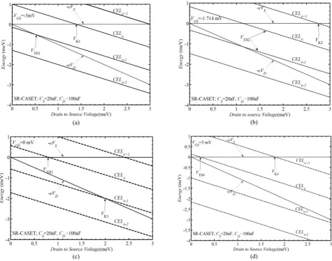
As an example, we have illustrated the I-V characteristics of a SR-CASET with CS=20 aF, CD=100 aF, and CG=20 aF (Case 2), for a more detailed discussion. Fig. 7 illustrates these I-V characteristics. The characteristics are drawn for the VGS values taken in all four regions defined in (25).
Fig. 6 Diamond diagram of an Al SET with Ech=100 meV at
T=4.2 K, which has good agreement with [14]
Fig. 7 I-V Characteristics of SR-CASET with RS=RD=160
kΩ, CG=20 aF, CS=20 aF and, CD=100 aF for VGS=–3mV, –1.714 mV, 0 mV and 3 mV
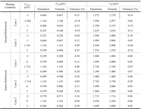
As seen from this figure, the threshold and kink voltages vary with the applied VGS, in a random fashion. Corresponding to VGSi for each case, designated by a positive integer i=1, 2, 3, or 4, there is a VTHi and a VKi, which can be explained by situation of the corresponding charging energy levels with respect to the source and drain Fermi levels. Figs. 8(a)-(d) illustrate four charging energy levels (CELn+1 , CELn , CELn-1, and CELn−2) corresponding to VGS1=−3 mV, VGS2=−1.714 mV, VGS3=0 mV, and VGS4=+3 mV, respectively. In each case, these four levels are compared with both SFL and DFL. As indicated in each case, there are at least two points at which two neighboring CELs cross over DFL and/or SFL. The point corresponding to smallest VDS, as we have mentioned earlier in Section 3, is the threshold voltage, and the next one is the kink voltage, as discussed in Section 4. Fig. 8 shows that as VGS increases from–3mV to +3 mV all four CELs are move towards lower energies. Since SFL and DFL in all four cases shown are the same, as CELs move towards lower energies their intercepts with the zero slope SFL move toward smaller values of VDS, while their intercepts with the negative slope DFL move in opposite direction. As illustrated in Fig. 8(a), the threshold, VTH1, and kink, VK1, voltages are the VDSvalues for which CELn−1 and
CELn cross over DFL and SFL, respectively.
The former corresponds to the situation in which an electron tunnels across the I/D junction, as also discussed in Section 3. Whereas, the latter corresponds to the situation in which an electron tunnels across the S/I junction, as also explained in Section 4. Fig. 8(a) also shows the next intercepting point is where CELn+1 and SFL cross over just at far end of the VDS window. Fig. 8(b) illustrates a case in which the first intercept shown in Fig. 8(a) has moved toward the right direction while the other two have moved toward the left direction. At the given VGS, the first and the second crossovers now occur at the same VDS=VTH2 that corresponds to the occurrence of the simultaneous tunneling across S/I and I/D junctions.
Meanwhile, the third point now represents the new kink voltage, VK2, which corresponds to tunneling of the next electron that occurs across the S/I junction. Increasing VGS beyond that of Fig. 8(b), as shown in Fig. 8(c), the alternates the roles of the crossovers, such that VTH3 and VK3 now correspond to VDS values for which CELn crosses SFL and CELn−1 intercepts DFL,
respectively. This means, under new biasing condition, tunneling across S/I junctions occurs before occurrence of tunneling across I/D junction. As also seen from this figure, the third point at which CELn+1 crosses SFL now corresponds to the second kink seen in the corresponding I-V characteristic of Fig. 7, near VDS=2.4 mV, which is related to the occurrence of the second tunneling across S/I junction, By increasing VGS, even further, a situation like that shown in Fig. 8(d) can occur in which the crossover between CELn−1 and DFL moves
beyond VDS=3 mV, and VTH4 and VK4 corresponds to the tunneling first two electrons both across S/I junction.
(a)
(c)
(b)
(d)
Fig. 8 VDS dependence of SFL, DFL, CELn+1 , CELn , CELn-1, and CELn−2 of a SR-CASET with RS=RD=160 kΩ, CG=20 aF, CS=20 aF and, CD=100 aF for (a) VGS=–3 mV, (b) –1.714 mV, (c) 0 mV and (d) 3 mV
6 Conclusion
In this paper, for the first time, we have derived a set of closed form equations for both threshold and kink voltages of single electron transistors with asymmetric source and drain capacitances, under various biasing conditions. By comparing the calculated values for both VTH and VK, obtained from the analytic formulas with those obtained from numerical simulation master equation based on orthodox theory, we have demonstrated the accuracy of our analytically derived formulas, in worst case, are better than 1%. We have also demonstrated the effect of the size and sign of inequality (i.e. ΔC=CS −CD) on the transistor ID-VDS characteristics under various biasing conditions.
References
[1] Waser R., Ed., Nanoelectronics and Information Technology-Advanced Electronic Materials and Novel Devices, 1st ed. Berlin :Wiley-VCH , 2003.
[2] Heinzel T., Mesoscopic Electronics in Solid State Nanostructures, WILEY-VCH Verlag GmbH & Co. KGaA,Weinheim, 2007.
[3] Grabert H. and Devoret M., Single Charge Tunneling, New York: Plenum, 1992.
[4] Inokawa H., Takahashi Y., “A Compact Analytical Model for Asymmetric Single-Electron Tunneling Transistors,” IEEE Trans.on Electron Dev., Vol. 50, pp. 455-461, 2003.
[5] Mahapatra S., Vaish V., Wasshuber C. and Banerjee K., “Analytical modeling of single electron transistor for hybrid CMOS-SET analog IC design,” IEEE Trans. on Electron Dev., Vol. 51, pp. 1772-83, 2004.
[6] Doiron C. B., Belzig W. and Bruder C., “Electrical transport through a single-electron transistor strongly coupled to an oscillator,” Phys. Rev. B, Vol. 74, pp. 205336, 2006.
Table 1 Comparison of threshold and kink voltages calculated from simulation with those obtained from our analytical derived
formulas for GR- and SR-CASETs at various VG/GS values
VTH (mV) VK (mV)
Biasing
Condition V(mV) G/GS
Simulation Formula Tolerance (%) Simulation Formula Tolerance (%)
–3 0.666 0.667 0.15 1.272 1.270 -0.16
–2.286 1.142 1.140 -0.18 2.596 2.597 0.04
–1 0.908 0.910 0.22 2.350 2.333 -0.72
Case 1
3 0.181 0.180 -0.55 1.635 1.630 -0.31
–3 0.221 0.220 -0.45 1.998 2.000 0.10
–1 0.666 0.667 0.15 1.999 2.000 0.05
1.143 1.142 1.143 0.09 2.920 2.900 -0.68
Ground Refer
en
ced
Case 2
3 0.399 0.400 0.25 1.555 1.550 -0.32
–3 0.199 0.200 0.50 1.800 1.800 0.00
0 0.799 0.800 0.13 1.999 2.000 0.05
1.714 1.142 1.143 0.09 2.742 2.740 -0.07
Case 1
3 0.499 0.500 0.20 1.399 1.400 0.07
–3 0.499 0.500 0.20 1.400 1.400 0.00
–1.714 1.142 1.143 0.09 2.742 2.750 0.29
0 0.799 0.800 0.13 1.999 2.000 0.05
Case 2
3 0.199 0.200 0.50 1.800 1.800 0.00
–2 0.570 0.571 0.18 1.713 1.714 0.06
0 1.142 1.143 0.09 3.428 3.430 0.06
Source Ref
eren
ced
Case 3
3 0.284 0.286 0.70 1.999 2.000 0.05
[7] Tanamoto T., “Quantum gates by coupled asymmetric quantum dots and controlled-NOT-gate operation,” Phys. Rev. A., Vol.61. pp. 022305, 2000.
[8] Gurvitz S. A. and Berman G. P., “Single qubit measurements with an asymmetric single-electron transistor,” Phys. Rev. B, Vol. 72, pp. 073303, 2005.
[9] Mizugaki Y., Kawai A., Moriya M., Usami K., Kobayashi T. and Shimada H., “Optimization of asymmetric single-electron transistor generating ac-induced dc current,” IEICE Electronic Express, Vol. 4, No. 11, pp. 345-350, 2007.
[10]Averin D. and Likharev K., “Coulomb blockade of single-electron tunneling and coherent oscillations in small tunnel junctions,” J. Low-Temp. Phys., Vol. 62, pp. 345–373, 1986.
[11]Wasshuber Ch., About Single Electron Devices and Circuits, Dissertation, Wien University, 1997. [12]Wasshuber Ch., Kosina H. and Selberherr S.,
“SIMON-A simulator for single-electron tunnel
devices and circuits,” IEEE Trans. On Computer-Aided Design, Vol. 16, pp. 937–944, Sep. 1997. [13] Wagner T., Krech W., Frank B. and Muhlig H.,
“Fabrication and Measurement of Metallic Single Electron Transistors,” IEEE Trans on Applied Superconductivity, Vol. 9, pp. 4277-4280, 1999. [14] Pashkin Y. A., Nakamura Y. and Tsai J. S.,“Room
temperature al single electron transistor made by electron beam lithography,” Appl. Phys. Lett., Vol. 76, pp. 2256-2258, 2000.
Ali Shahhoseini was born in February, 1967
in Iran, Tehran. He received his B.Sc. degree in Electrical Engineering from Isfahan Technology University in 1989, and his M.Sc. degree from Tarbiat Modarres University in 1995, respectively. Mr. Shahhoseini is currently Ph.D. candidate in the Department of Electrical Engineer-ing at the Islamic Azad University - Science and Research Branch, Tehran, Iran. His current research interests are in the area of Simulation of nanoelectronic Devices.
Kamyar Saghafi was born in Tehran, Iran, on
December 19, 1963. He received the B.Sc. degree in electrical engineering in 1991, from Iran University of Science and Technology, and the MS degree in 1994 and Ph.D. degree in 1999 in electrical engineering both from Tarbiat Modares University, Iran. In 1999 he joined the department of Electronic Engineering of Shahed University, Iran. He has been working on simulation of submicron semiconductor devices. He is presently working on numerical modeling and simulation of nano devices such as carbon nanotube field effect transistors, single electron transistors and nanowire transistors.
Mohammad Kazem Moravvej-Farshi was
born in Yazd, Iran, in 1952. He received the B. Sc. and the M. A. degrees in physics from Sharif University of Technology (SUT), Tehran, Iran, in 1976, and the University of Southern California (USC), Los Angeles, California, in 1978, respectively, the M. Sc. and the Ph. D degrees in electronics from the University of California at Santa Barbara (UCSB), in 1980, and the University of New South Wales (UNSW), Sydney, Australia, in 1987, respectively. From 1980 to 1984, he was a member of research staff with the Division of Microwave, Iran Telecommunication Research Center (ITRC). He joined Tarbiat Modares University (TMU) in 1987, where he is currently a Professor of Electronics. He has translated from English to Farsi four books in the field of semiconductor devices and one in laser electronics. His last translation in 2004 was selected as the best translation of the year in the field of engineering and applied sciences. M. K. Moravvej-Farshi was elected as one of the two most prominent professors of 2002 in the field of electrical engineering, nationwide. From October 1993 to June 1994, he was a Visiting Professor with the School of Electrical Engineering and Computer Science, University of Nottingham; Nottingham, U.K. Professor Moravvej Farshi is currently a senior member of IEEE, and also a member of OSA. He is also one of the founders of the Optics and Photonics Society of Iran (OPSI). He has been elected IEEE Iran Section Vice president for the period 2009-2011.
Rahim Faez received B.S. degree from
Sharif University of Technology in 1977 and the M.S. and Ph.D. degrees from UCLA in 1979 and 1985 respectively. Then he joined Sharif University of Technology and currently he is Associate professor in there. His research interests include design and simulation of advanced semiconductor nano and quantum devices.

![Fig. 6 Diamond diagram of an Al SET with TEch=100 meV at =4.2 K, which has good agreement with [14]](https://thumb-us.123doks.com/thumbv2/123dok_us/216760.2016152/7.595.61.274.544.708/fig-diamond-diagram-al-set-tech-good-agreement.webp)