Design and Analysis of 5-T SRAM Cell in 32nm
CMOS and CNTFET Technologies
G. Boopathi Raja
Department of ECE, Velalar College of Engineering and Technology, Erode, TN, India Email: [email protected]
M. Madheswaran
Mahendra Engineering College, Namakkal Dt, TN, India Email: [email protected]
Abstract—MOS transistor play a vital role in today VLSI technology. In CMOS based design, symmetry should be followed in circuit operation. Most of the complex circuits are allowed to design in CMOS, however, there are several drawbacks present in this complementary based design. CMOS has lost its credentiality during scaling beyond 32nm. Scaling down causes severe short channel effects which are difficult to suppress. As a result of these effects, many researchers are undergone to find suitable alternate devices. Therefore, it is necessary to find alternative way suitable for particular design, instead of CMOS. Some of the research includes Multi Gate Field Effect Transistor (MuGFET) like FinFET, Nano tubes, Nano wires etc. In most of the modern design is based on Carbon nanotube because of its superior properties interms of power consumption, leakage power, delay etc. In this paper, we mainly focus on designing SRAM cell in CMOS, CNFET. In this work, 6T SRAM (symmetric structure) and 5T SRAM (asymmetric) cell in 32nm CMOS as well as CNTFET technologies and its performance has to be compared.
Index Terms—carbon nanotube, CMOS, data retention, read disturb, static RAM, write-ability
I. INTRODUCTION
In a 6 transistor Static RAM cell, the two cross-coupled PMOS pull-up devices retain the value written into a cell, in [1], [2] and [3]. These cross-coupled p-devices are designed to be strong enough to retain a value in the cell indefinitely without any external refresh mechanism. However, if the p-devices are too weak due to a fabrication defect or a connection to either of the p devices is missing, the static RAM (cell will no longer be able to hold its data indefinitely, in [4], [5] and [6]. The resulting fault in defective cell is referred to as a data retention fault (DRF) or a cell stability fault, depending its on severity. Thus all static RAMS require some form of data retention and cell stability testing.
Traditionally, testing large static CMOS memory arrays for data retention faults (DRFs) and cell stability faults has been a time consuming and expensive effort. Existing test methods have also been partial in their test coverage.
Manuscript received April 14, 2013; revised October 5, 2013
The algorithmic test methods currently used for detecting these faults are primarily functional in nature; that is they check the cell stability or retention in a functional manner.
These methods are time consuming and require extensive characterization of silicon to determine the worst case test conditions. The following functional tests are commonly used by memory manufacturers, [4]:
Pause (Data Retention): Write a background to the array, then after a pause on the order of 100 ms read the array to determine if any cell has changed state;
Read disturb: Write a background to the array, then read the array at a lower or higher Vcc but ignore the data (i.e. tester strobe disabled), thereafter read the array to determine if any cell has changed state;
Long Write: Write a background to the array, then perform a long write on a row, then read all other rows of the array to determine if any cell has changed state. Repeat for all rows in the array.
II. READ STABILITY AND WRITEABILITY OF THESRAM CELL
A. The SRAM Cell Read Stability
Data retention of the SRAM cell, both in standby mode and during a read access, is an important functional constraint in advanced technology nodes. The cell becomes less stable with lower supply voltage (Vdd), increasing leakage currents and increasing variability, all resulting from technology scaling. The stability is usually defined by the SNM as the maximum value of DC noise voltage(Vn) that can be tolerated by the SRAM cell without changing the stored bit. The two DC noise voltage sources (Vn) are placed in series with the cross-coupled inverters and with worst-case polarity at the internal nodes of the cell.
The Write-Ability of the SRAM Cell
much energy in pulling down the bit-line voltage to 0 V. The write-trip point defines the maximum voltage on the bit-line, needed to flip the cell content. The write-trip point is mainly determined by the pull-up ratio of the cell while the read stability is determined by the cell ratio of cell; this results in the well-known conflicting design criteria. The SRAM N-curve can also be used as alternative for the write-ability of the cell, since it gives indications on how difficult or easy it is to write the cell.
III.CNTFETDEVICES
As one of the promising new devices, CNTFET (Carbon Nanotube Field Effect Transistor) avoid most of the fundamental limitations for traditional silicon devices, in [4], [7] and [8]. All the carbon atoms in CNT are bonded to each other with sp2 hybridization and there is no dangling bond which enables the integration with high-k dielectric materials.
A. Carbon Nano-Tube (CNT)
A single-walled carbon nanotube (SWCNT) can be visualized as a sheet of graphite which is rolled up and joined together along a wrapping vector Ch=na1 + ma2 , where [a1; a2 ] are lattice unit vectors, and the indices (n, m) are positive integers that specify the chirality of the tube. The length of Ch is thus the circumference of the CNT, which is given by equation (1),
Ch = a√ (1) Single-walled CNTs are classified into one of their groups, depends on the chiral number (n, m):
(1) armchair (n1 = n2),
(2) zigzag (n1 = 0 or n2 = 0), and (3) chiral (all other indices).
The different ways for rolling graphene sheet to make carbon nanotube is to be shown below (Fig. 1 & Fig. 2):
Figure 1.Different ways for rolling graphene sheet
The diameter of the CNT is given by the formula
DCNT= Ch/π
The electrons in CNT are confined within the atomic plane of graphene. Due to the quasi- 1D structure of CNT, the motion of the electrons in the nanotubes is strictly
restricted. Electrons may only move freely along the tube axis direction. As a result, all wide angle scatterings are prohibited. Only forward scattering and back scattering due to electron phonon interactions are possible for the carriers in nanotubes. The experimentally observed ultra long elastic scattering mean-free-path (MFP) (approximately 1µm) implies ballistic or near-ballistic carrier transport. High mobility, typical in the range of 103 (approx. 104cm2=V/s˙) which are derived from conductance experiments in transistors. Theoretical study also predicts a mobility of approx. 104cm2=V·s for semiconducting CNTs.
Figure 2. CNT (Carbon-nanotube) types
The current carrying capacity of multi-walled CNTs are demonstrated to be more than 109A=cm2 about 3 orders higher than the maximum current carrying capacity of copper which is limited by the electron migration effect, without performance degradation during operation well above room temperature. The superior carrier transport and conduction characteristic makes CNTs desirable for nanoelectronics applications, e.g. interconnect and nanoscale devices.
B. CNTFET Technology
CNTs are sheets of graphene rolled into tubes; depending on the chirality (i.e., the direction in which the grapheme sheet is rolled), a single-walled CNT can be either metallic or semiconducting, in [9]. It is clearly shown in Fig. 2. Semiconducting carbon nano-tubes have attracted widespread attention of device/circuit designers as an alternative possible channel implementation for high-performance transistors.
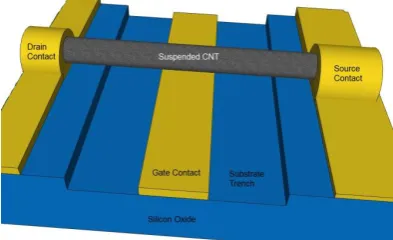
The CNT channel region is undoped, while the other regions are heavily doped, thus acting as the source/drain extended region and/or interconnects between two adjacent devices. Carbon nanotubes are high-aspect-ratio cylinders of carbon atoms. The electrical properties of a single wall carbon nanotube (SWNT) offer the potential for molecular-scale electronics; a typical semiconducting single-wall carbon nanotube is 1.4nm in diameter with a 0.6eV bandgap (the bandgap is inversely proportional to the diameter). Recent carbon nanotube field effect transistors (CNTFETs) have a metal carbide source/drain contact and a top gated structure (Fig. 3) with thin gate dielectrics.
The contact resistance and the subthreshold slope of a CNTFET are comparable to those of a silicon MOSFET. While a silicon FETs current drive is typically measured in current per unit device width (e.g. µA=µm), the CNTFETs current is measured in current per tube (as reflecting the structure of the CNTFET as an array of equal carbon nanotubes with constant spacing and fixed diameter).
C. CNTFET-Characteristics and Operation
The operation principle of carbon nanotube field-effect transistor (CNTFET) is similar to that of traditional silicon devices. This three (or four) terminal device consists of a semiconducting nanotube, acting as conducting channel, bridging the source and drain contacts. The device is turned on or off electrostatically via the gate. The quasi-1D device structure provides better gate electrostatic control over the channel region than 3D device (e.g. bulk CMOS) and 2D device (e.g. fully depleted SOI) structures. In terms of the device operation mechanism,
(a) SB-CNTFET
Figure 4.The energy-band diagram for (a) SB-CNTFET (b) MOSFET- like CNTFET
CNTFET can be categorized as either Schottky Barrier (SB) controlled FET (SBCNTFET) or MOSFET-like FET.
The conductivity of SB-CNTFET is governed by the majority carriers tunneling through the SBs at the end contacts. The on-current and thereby device performance of SB-CNTFET is determined by the contact resistance due to the presence of tunneling barriers at both or one of the source and drain contacts, instead of the channel conductance, as shown by Fig. 4(a).
The SBs at source/drain contacts are due to the Fermi level alignment at the metal-semiconductor interface. Both the height and the width of the SBs, and therefore the conductivity, are modulated by the gate electrostatically. SB-CNTFET shows ambipolar transport behavior.
The work function induced barriers at the end contacts can be made to enhance either electron or hole transport. Thus both the device polarity (n-type FET or p-type FET) and the device bias point can be adjusted by choosing the appropriate work function of source/drain contacts. On the other hand, MOSFET like CNTFET exhibits unipolar behavior by suppressing either electron (pFET) or hole (nFET) transport with heavily doped source/drain. The non tunneling potential barrier in the channel region, and thereby the conductivity, is modulated by the gate-source bias (Fig. 4(b)).
IV. 6TSRAMCELL
The schematic diagram of 6T SRAM cell is shown in Fig. 5. During read, the WL voltage VWL is raised, and the memory cell discharges either BL (bit line true) or BLB (bit line complement), depending on the stored data on nodes Q and BQ, in [4], [10], [11] and [12]. A sense amplifier converts the differential signal to a logic-level output. Then, at the end of the read cycle, the BLs returns to the positive supply rail. During write, VWL is raised and the BLs are forced to either VDD (depending on the data), overpowering the contents of the memory cell.
Figure 5. Schematic of 6T SRAM Cell
During hold, VWL is held low and the BLs are left floating or driven to VDD. Each bit in an SRAM is stored on four transistors that form two cross-coupled inverters. This storage cell has two stable states, which are used to denote 0 and 1.
typical SRAM uses six MOSFETs to store each memory bit and the explanation here is based on the same. Access to the cell is enabled by the word line which controls the two access transistor M5 and M6 which, in turn, control whether the cell should be connected to the bit lines: BL and BLB. They are used to transfer data for both read and write operations. Although it is not strictly necessary to have two bit lines, both the signal and its inverse are typically provided to improve noise margins. During read accesses, the bit lines are actively driven high and low by the inverters in the SRAM cell. This improves SRAM bandwidth compared to DRAMs. A SRAM cell has three different states it can be in: standby where the circuit is idle, reading when the data has been requested and writing when updating the contents.
V. 5TSRAMCELL
The 5T cell has only one access transistor ‘N3’ and a single bitline ‘BL’, which is shown in Figure 6. Writing of ‘1’ or ‘0’ into the 5T cell is performed by driving the bitline to Vcc or Vss respectively, while the wordline is asserted at Vcc. The writability of the cell is ensured by a different cell sizing strategy. The trip-point of the inverter P2-N2 has been decreased, while the trip-point of the inverter P1-N1 has been increased. Further, the pass-transistor N3 is sized to support both write and read operation. The sizes of transistors are normally selected based on Table I.
Since the 5T SRAM cell is writable at Ver=Vwr=Vcc, a non-deshuctive read operation requires a bitlineprecharge voltage, Vpc, where Vss < Vpc < Vcc. This isin contrast to the conventional 6T SRAM bitlines, whichare precharged at Vcc before a read operation.
The static noise margin is defined as the maximum noise that can be tolerated at the input of the SRAM without changing its status, in [13]. It is given by the size of the
smallest square that can be inscribed in the butterfly curve of the SRAM.
Figure 6. Asymmetric 5T SRAM Cell TABLE I. NORMALIZED BITCELL SIZING
P1 P2 N1 N2 N3 Objective
1.27/1 1.27/1 7.67/1 1.27/1 2.91/1.04 Max RSNM
1.27/1.35 1.27/1 6.73/1 4/1 2.91/1.04 Balanced
1.27/1 4.95/1 4/1 1.27/1 2.91/1.04 Max HSNM
1.27/1 1.27/1 5.45/1 2.54/1.35 2.91/1.04 Max WSNM 1.27/1 1.27/1 7.67/1 1.27/1 3.64/1.04 Min leakage
Write margin is found as the maximum bit line voltage at which the write operation is obtained when the bit line voltage is changed from VDD to 0V.
The read delay is defined as time delay between 50% level change in the word line signal to 50% level change in the output of the sense amplifier. Generally the differential type of sense amplifier results in less delay compared to single ended buffer.
However, the delay in the single ended buffer is improved by choosing inverters with sizes in the increasing order reduced bit line capacitance.
VI.SIMULATION RESULTS
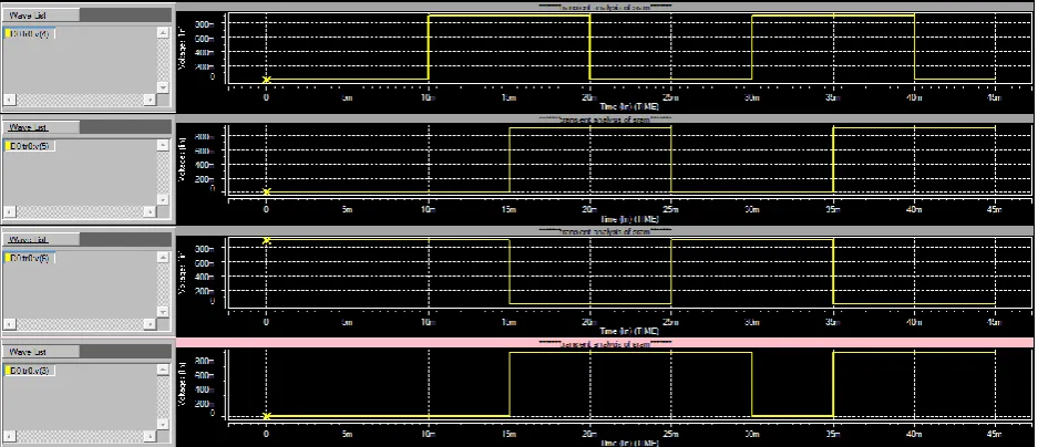
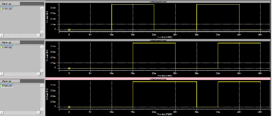
Simulation waveform for 5-T as well as 6-T SRAM Cell based on 32nm CMOS and CNTFET is shown in below:
Figure 8.Simulation waveform for 5-T SRAM cell in 32nm CMOS technology
Figure 9.Simulation waveform for 6-T SRAM cell in 32nm CNTFET technology
TABLE II. PERFORMANCE COMPARISON OF 6T AND 5TSRAMCELL IN CMOS AND CNTFETTECHNOLOGY
Parameters 6T-SRAM Cell 5T-SRAM Cell
Technology used CMOS based design CNTFET based
design CMOS based design
CNTFET based design
Average power consumption 16.605nW 6.211 pW 12.43 uW 4.3912nW
Total voltage source power dissipation 5.5079 nW 32.90 pW 2.0965nW 1.617nW
Average delay 0.2964 us 2.5049 ns 7.21 us 0.91 s
CMOS and CNFET based 6-T as well as 5-T SRAM cell is designed at 32nm scale range and allowed to simulate by using HSPICE tool, using model files from [14], [15] and [16]. Simulation waveforms are shown in above figures (Fig. 7, Fig. 8, Fig. 9, Fig. 10) respectively. Performance of 6T and 5T SRAM cell is compared based on average power consumption, average power dissipation and average delay is shown in Table II.
VII. CONCLUSION
From the above table, it is clear that CNTFET based design is more efficient than CMOS based design in all aspects such as cost, power consumption, power dissipation and average delay. CNTFET based 6T SRAM cell consumes more power, dissipates large amount of power than that of CNTFET based 5T SRAM cell. However, delay is more in asymmetric based 5T SRAM cell. This can be reduced by proper symmetric or balanced design.
REFERENCES
[1] B. Raj, A. K. Saxena, and S. Dasgupta, "Nanoscale FinFET based SRAM cell design: Analysis of performance metric, process variation, underlapped FinFET and temperature effect," IEEE Circuits and Systems Magazine, pp. 38-50, Aug. 2011.
[2] N. K. Jha and D. Chen, Nanoelectronic Circuit Design, Springer, 2011.
[3] T. P. Haraszti, CMOS Memory Circuits, Kluwer Academic Publishers, 2002.
[4] G. B. Raja and M. Madheswaran, "Design and performance comparison of 6-T SRAM cell in 32nm CMOS, FinFET and CNTFET technologies," International Journal of Computer Applications, vol. 70, no. 21, May 2013.
[5] S. M. (Steve) Kang, Y. Leblebigi, CMOS Digital Integrated Circuits: Analysis and Design, McGraw-Hill, 2rd Ed, 1998. [6] K. S. Yeo and K. Roy, Low-Voltage, Low- Power VLSI Subsystems,
McGraw-Hill, New York, 2005.
[7] J. Deng and H. S. P. Wong, "A compact SPICE model for carbon nanotube field-effect transistors including nonidealities and its application-part I: Model of the intrinsic channel region," IEEE Transactions on Electron Devices, vol. 54, no. 12, pp. 3I86-3194, Dec. 2007.
[8] J. Deng and H. S. P. Wong, "A compact SPICE model for carbon nanotube field-effect transistors including nonidealities and its application-part II: Full device model and circuit performance benchmarking," IEEE Transactions on Electron Devices, vol. 54, no. 12, pp. 3195-3205, Dec. 2007.
[9] J. Deng, H.-S. P. Wong, “A circuit-compatible SPICE model for enhancement mode carbon nanotube field effect transistors,”
Simulation of Semiconductor Processes and Devices, 2006.
[10] J. Y. S. Balasubramanium, “Design of sub-50 nm FinFET based low power SRAMs,” Semicond. Sci. Technol., vol. 23, p. 13, 2008. [11] Z. Guo, S. Balasubramanian, R. Zlatanovici, T. J. King, and B.
Nikolic, “FinFET based SRAM design,” in Proc. Int. Symp. Low Power Electronicsand Design, 2005, pp. 2–7.
[12] H. Pilo, “SRAM design in the nanoscale era,” in Proc. Int. Solid State Circuits Conf., 2005, pp. 366–367.
[13] E. Seevinck, F. J. List, and J. Lohstoh, Static-Noise Margin Analysis of MOS SRAM Cells. JSSC, 1987, pp. 366-167.
[14] International Technology Roadmap for Semiconductors (ITRS). San Jose, CA: Semiconductor Industry Association, 2007. [15] Predictive technology model for 32 nm CMOS technologies.
[Online]. Available: http://www.eas.asu.edu/~ptm
[16] Stanford University CNFET Model Website. [Online]. Available : http://nano.stanford.edu/model.php?id=23
Dr. M. Madheswaran has obtained his Ph.D. degree in
Electronics Engineering from Institute of Technology, Banaras Hindu University, Varanasi (now it is named as IIT-BHU) in 1999 and, at present, pursuing his second Ph.D in Human Resource Management (Emotional Intelligence) from Anna University, Chennai, Tamil Nadu. He completed his M.E degree in Microwave Engineering from Birla Institute of Technology, Ranchi, India and B.E. degree in ECE from Mohammed Sathak Engineering College, Kilakarai. He has started his teaching profession in the year 1991 to serve his parent Institution Mohd. Sathak Engineering College, Kilakarai. Currently, he served as the principal of Mahendra Engineering College, Namakkal. Before that he served as the Professor and Principal in Muthayammal Engineering College, Rasipuram and Professor in KSR College of Technology, from 1999 to 2001 and PSNA College of Engineering and Technology, Dindigul from 2001 to 2006. He has been awarded “Young Scientist Fellowship”, “Senior Research Fellowship” and “Best citizen of India”. He has visited many countries like USA, Japan, Singapore, Malaysia, Egypt, Taiwan, China, Thailand, Dubai, and Hong Kong for his professional research in electronic engineering. He has flourished around 115 journal publications and 51 conferences. Dr. Madheswaran is an Senior Member of IEEE, fellow of IETE and IE India, Life Member of Indian Society for Technical Education (ISTE) and Member in VLSI Society of India. His field of interest includes semiconductor devices, m ed i c a l i ma gi n g, n a n o e l ec t r on i c s , mi c r o wa v e e l ec t r on i c s , optoelectronics and signal processing. Also, He is the Chairman of IEEE India EDS Chapter and Vice-Chairman of IEEE India SSCS Chapter.
G. Boopathi Raja has obtained his B.E. degree in