Available Online at www.ijpret.com 112
INTERNATIONAL JOURNAL OF PURE AND
APPLIED RESEARCH IN ENGINEERING AND
TECHNOLOGY
A PATH FOR HORIZING YOUR INNOVATIVE WORK
PERFORMANCE ANALYSIS OF 64-BIT HYBRID ADDER DESIGN BASED ON
RADIX-4 PREFIX TREE STRUCTURE
S. MURTHY1, A. GANGADHARAM2
1.M. Tech Student, DSCE 2nd DEPT OF ECE, KMM Institute of Technology and Science, Ramireddipalle, Chandragiri, Mandal, Tirupati,
Chittoor, Andhra Pradesh.
2.Asst. Professor, DEPT OF ECE, KMM Institute of Technology and Science, Ramireddipalle, Chandragiri, Mandal, Tirupati, Chittoor, Andhra
Pradesh.
Accepted Date: 27/08/2015; Published Date: 01/10/2015
\
Abstract: - Addition is important in many of data path subsystems. The primary factor for any design is to reduce the power dissipation and to increase the performance. To achieve the performance and to reduce the power dissipation, selection of adder topology is an important thing. The use of parallel prefix adders (PPA’s) increases the performance by reducing the power dissipation. A 64-bit hybrid adder design is proposed by using both radix-4 prefix tree structure and carry select adder for low voltage and low powe r applications. In order to optimize the features of this adder, some design issues are concerned including optimal layout for CMOS group generate/propagate circuit to reduce area, design of carry bypass adder (CBA) without conflict to boost speed, carry s elect adder (CSA) design with speed and area efficiency, and so on.
Keywords:Low Voltage; Low Power; Hybrid Adder; Carry Select Adder; Prefix Tree Structure
Corresponding Author: MR. S. MURTHY
Access Online On:
www.ijpret.com
How to Cite This Article:
Available Online at www.ijpret.com 113
INTRODUCTION
Addition is the most fundamental operation of arithmetic logic unit (ALU) and floating point unit (FPU) in microprocessors. With the rapid growth in portable electronic equipments and mobile communication devices, demand to low voltage and low power technology for VLSI applications is great increasing. In general, high speed adder includes carry lookahead adder (CLA), carry select adder (CSA), carry bypass adder (CBA), conditional sum adder and later developed parallel prefix adder (PPA).
Different prefix algorithms and tree topologies of PPAs have been implemented for solving delay, area, and power efficiencies. Design of an appropriate tree topology is a trade-off among the fan-out, the wiring count and the logic level. Recently, several high-performance 64-bit adders have been reported. The high-speed 64-bit adder was hybrid sparse redix-4 prefix tree and CSA based on energy-delay optimization methodology, however its implementation by using domino CMOS logic consumes higher power dissipation. Branch-based logic (BBL) is applied in another high-performance 64-bit CSA to minimize power-delay product. The drawback of such a design is that the speed and area are still limited. In this paper, a 64-bit hybrid adder is proposed to combine both prefix tree structure (PTS) and CSA for fetching low voltage and low power features. The three stages prefix tree of the 64-bit hybrid adder computes carries, and then the CSA with add-one circuit selects sums by these carries. Otherwise, the CBA has been added at the third stage of the PTS to diminish fan-ins, fan-outs, wiring counts and transistor counts. With respect to low voltage low power method, complementary metal oxide semiconductor (CMOS) logic, transmission gate (TG) logic, and pass transistor logic (PTL) are applied in proposed design to fetch full swing operation at each node.
I. PARALLEL-PREFIX ADDER STRUCTURE
Parallel-prefix structures are found to be common in high performance adders because of the delay is logarithmically proportional to the adder width.
PPA’s basically consists of 3 stages
• Pre computation
• Prefix stage
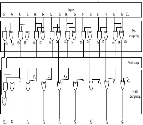
Available Online at www.ijpret.com 114 The Parallel-Prefix Structure is shown in figure 1.
Fig. 1. Parallel-Prefix Structure with carry save notation
A.Pre computation
In pre computation stage, propagates and generates are computed for the given inputs using the given equations.
B.Prefix stage
In the prefix stage, group generate/propagate signals are computed at each bit using the equations.
C.Final computation
In the final computation, the sum and carryout are the final output.
Available Online at www.ijpret.com 115 The generate/propagate signals can be grouped in different fashion to get the same correct carries. Based on different ways of grouping the generate/propagate signals, different prefix architectures can be created.
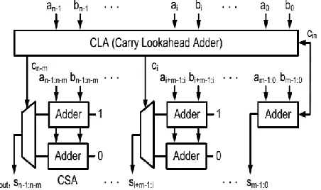
II. GENERAL HYBRID ADDER ARCHITECTURE
In the binary addition, let the two n-bit operands be denoted as A = and B = and the sum as S = . For faster adder computation, the carry generation (g) is defined as , and the carry propagation (p) is defined as . Let be the least significant bit (lsb) of the carry input, and the carry input at
the i+1-th bit position is = . And then the sum output at the i-th bit position is .
Figure 2. General hybrid adder architecture.
The CLA is the most commonly used scheme to improve speed by reducing the amount of time required to determine carries. The high performance of a CLA is gained from generating all incoming carries in parallel to prevent the need of waiting the correct incoming carries generated from corresponding lower significant bit. However, the drawback of CLA is with heavy and irregular area overhead. The CSA consists of two duplications of ripple carry adder in each stage, one performs the addition with =0, whereas the other does this with =1. Then, the final sum and carry out are selected by the real value of carry through
multiplexers (MUXs). Although CSA speeds up the addition operation, it has the drawback of increasing area overhead.
Available Online at www.ijpret.com 116 shown in Figure 2; it consists of the CLA and the CSA. The CLA generates partial carry to reduce the area complexity, and then the carry signals go through the MUXs of the CSA to select the final sum.
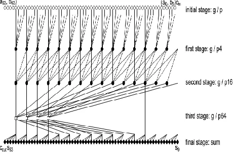
III.PROPOSED 64-BIT HYBRID ARCHITECTURE
The proposed hybrid adder, as shown in Figure 3, is made up of three modules including the generate/propagate generation (GPG), the prefix tree structure (PTS) and the CSA with add-one circuit. The initial stage of the GPG generates individual generate and propagate signals for each bit position. The middle stage of the PTS computes some specific carries to the next stage for the CSA. The final stage of the CSA with add-one circuit selects the proper sum as the output. We take advantage of the initial stage of sharing generate and propagate signals in both PTS and CSA blocks to reduce the hardware overheads and to achieve more compact area.
Figure 3. Block diagram of proposed hybrid adder architecture
A.Proposed 64-bit Hybrid Adder
For a PPA, the carry computation approach dominates the overall performance. In order to fetch faster addition, many parallel prefix tree topologies have been developed to give a good trade-offs among speed, area and power. The more efficient way is implementing parallelizable prefix computation by taking advantage of the associative operator “o”. The generate (g) and propagate (p) signals can be defined as follow:
(g, p)o(g’, p’) =(g + pg’, pp’) (1)
Giving a series of bits i…j…k, the group generate/propagate pair ( , ) can be expressed in
Available Online at www.ijpret.com 117 ( , ) = ( , o…o ( , ) o ( , )o( , )o…o( , ) (2)
Similarly, recurrence forms for group generate/propagate pair ( , ) can be derived by “o”
from two pairs as following.
( , ) = ( , ) o ( , ) (3)
Available Online at www.ijpret.com 118
Figure 4. Proposed 64-bit hybrid adder
B.The Group G/P Functions
The group generate/propagate (g/p) functions for each group of four bits, depicted as black circles of the first and the second stages in Fig. 4, are expressed as:
(4)
(5)
IV.SIMULATION RESULTS
Available Online at www.ijpret.com 119
RTL Schematic diagram
Available Online at www.ijpret.com 120
Simulation output waveform
V. CONCLUSIONS
A transistor-level based method for designing low voltage and low power 64-bit hybrid adder has been presented. The proposed hybrid adder is composed of the redix-4 prefix tree structure and the CSA to benefit the high speed. In design issues, reduced area overhead is used to diminish power dissipation, and all full voltage swing operations is considered to lower supply voltage needed.
REFERENCES
1. Harris, “A Taxonomy of Parallel Prefix Networks,” Conference Record of the Thirty-Seventh Asilomar Conference on Signals, Systems and Computers, vol. 2, pp. 2213-2217, 9-12 Nov. 2003. 2. R. Zlatanovici, S. Kao and B. Nikolic, “Energy–Delay Optimization of 64-Bit Carry-Lookahead Adders With a 240 ps 90 nm CMOS Design Example,” IEEE Journal of Solid-State Circuits, vol. 44, no. 2, pp. 569-583, Feb. 2009.
3. A. Neve, H. Schettler, T. Ludwig and D. Flandre, “Power-Delay Product Minimization in High-Performance 64-bit Carry-Select Adders,” IEEE Transactions on Very Large Scale Integration (VLSI) Systems, vol. 12, no. 3, pp. 235-244, Mar. 2004.
4. R. P. Brent and H. T. Kung, “A Regular Layout for Parallel Adders,” IEEE Transactions on Computers, vol. C-31, no. 3, pp. 260-264, Mar. 1982.
Available Online at www.ijpret.com 121 6. J. M. Rabaey, A. Chandrakasan and B. Nikolic, “Digital Integrated Circuits: A Design Perspective, 2nd Edition,” Prentice Hall, 2003.
7. B. R. Zeydel, D. Baran and V. G. Oklobdzija, “Energy-Efficient Design Methodologies: High-Performance VLSI Adders,” IEEE Journal of Solid-State Circuits, vol. 45, no. 6, pp. 1220-1233, Jun. 2010.
8. T. Uehara and W. M. Vancleemput, “Optimal Layout of CMOS Functional Arrays,” IEEE Transactions on Computers, vol. C-30, no. 5, pp. 305-312, May 1981.
9. T. Sato, M. Sakate, H. Okada, T. Sukemura and G. Goto, “An 8.5- ns 112-b transmission gate adder with a conflict-free bypass circuit,” IEEE Journal of Solid-State Circuits, vo. 27, no. 4, pp. 657-659, Apr. 1992.
10.T.-Y. Chang and M.-J. Hsiao, “Carry-Select Adder Using Single Ripple-Carry Adder,” Electronics Letters, vol. 34, no. 22, pp. 2101-2103, 1998.