Annealing Effects on Structures and Morphologies of Fe
/
Si Core
Shell Clusters
Kenji Sumiyama
1,+1, Satoshi Kadowaki
2,+2, Yuichiro Kurokawa
2,+3,
Naokage Tanaka
2,+4, Ryoji Katoh
2,+5and Takehiko Hihara
21School of Science and Engineering, Tokyo Denki University, Hiki-gun, Saitama 350-0394, Japan
2Department of Materials Science and Engineering, Nagoya Institute of Technology, Nagoya 466-8555, Japan
Transmission electron microscopy, X-ray diffraction and electrical resistivity have been observed for annealed Fe/Si coreshell clusters and their assemblies in comparison with those for annealed Fe and Si clusters. Fe clusters are wholly oxidized, where voids are formed in the central regions. Si clusters are not wholly oxidized, keeping a diamond-like structure, where voids are scarcely formed in the central regions because the initially-oxidized surfaces play roles of passive layers and protect the cores from oxidations. In FeSi core/Si shell clusters, SiOX
thin layers are also formed on Si shell surfaces, protecting Si shells and FeSi cores from further oxidations. FeSi core regions maintain a bcc structure, where no ordered phase is detected probably due to the chemical heterogeneity among these clusters and the surface segregation of Si atoms. Excess vacancies are accumulated to become voids between FeSi cores and Si-shells. [doi:10.2320/matertrans.M2012383]
(Received November 16, 2012; Accepted January 29, 2013; Published March 25, 2013)
Keywords: ironsilicon nanoparticles, cluster assembly, coreshell morphology, thermal stability, oxidation behavior
1. Introduction
Nanometer size clusters are comparable to basic units of material functions and promising for building blocks of nano-scale structure-controlled materials.1,2) Using a plasma-gas-condensation-cluster-deposition (PGCCD) system with a single glow discharge source, we can obtain uniform size metal clusters by setting elemental targets,3)and alloy clusters
by setting two different metal targets face to face and supplying them different electric powers.4) Blending of two
different element clusters is a next challenge because their contact interfaces often yield novel catalytic properties. Using PGCCD systems with two glow discharge sources, we can prepare several hybrid clusters by adjusting a partition plate between two glow discharge sources: juxtaposition of two different clusters, formation of coreshell and alloy clusters, etc.510) If collision times of Fe and Si atoms are delayed with setting the partition plate, small Fe-rich clusters are randomly distributed with aggregated Si clusters. On the other hand, if their collision times are expedited without setting the partition plate, bcc Fe cores are surrounded by small amorphous Si shells.6,11,12)Their detailed structures and
morphologies are influenced by the back ground vacuum conditions of PGCCD systems. When the deposition chamber is only evacuated by a mechanical booster pump (a poor background-vacuum-condition), sputtered Si atoms and Si cluster nuclei are more easily oxidized than sputtered Fe atoms and Fe cluster nuclei. Since the affinities of SiO are much higher than those of FeSi,1315) Si and Fe nuclei neither merge nor form an alloy at their collision events. When the deposition room is evacuated by a turbo molecular
pump (a good background-vacuum-condition), Fe and Si cluster nuclei collide with each other at the growth stage and FeSi alloy cores are covered by amorphous Si shells.11,12) Since the surface energy of Si is much lower than that of Fe,16,17) Si cluster nuclei cover Fe cluster nuclei and they merge at around their contact interfaces. In the FeSi alloy cores, chemically heterogeneous bcc solid solutions are obtained, while a bcc ordered phase Fe3Si and intermetallic
compound phases, Fe5Si3, FeSi and FeSi2are not detected18)
probably because their cohesive energy of Fe and Si cluster nuclei are effectively extracted via collisions with inert gas atoms and atomic diffusions of Fe and Si atoms are depressed.
Then, it is interesting to study phase stability and morphological changes in Fe/Si hybrid clusters by heat treatments. It is also topical to study their characteristic oxidation behaviors because void formation in clusters and hollow clusters have been observed in nanoparticles and island-like films.1921)This paper briefly describes structural and morphological changes, and oxidation behaviors in annealed FeSi core/Si shell hybrid clusters in comparison with those in Fe and Si clusters.
2. Experimental Procedures
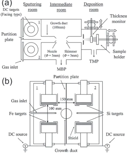
Figure 1 shows the PGCCD system with two DC glow discharge sources, whose details were described in other papers.911) Fe and Si (doped with 10¹3at%Al) disc plates
(80 mm in diameters and 5 mm in thicknesses) were set on the target holders of the sputtering rooms 1 and 2, which were evacuated down to 3©10¹4Pa. The intermediate room was evacuated down to 3©10¹5Pa by a compound molecular pump (CMP; not shown in Fig. 1) and the deposition room down to 6©10¹6Pa by a turbo molecular pump (TMP). For glow discharge sputtering, CMP was shut down and argon gas (99.9999 vol%) was introduced through a gas-inlet with a variable leak valve and the intermediate room was evacuated by a mechanical booster pump (MBP; 0.16 m3/s). The argon
gas flow rate was kept at 3.3©10¹6m3/s. It led to the
+1Corresponding author, E-mail: sumiyama@mail.dendai.ac.jp
+2Graduate Student, Nagoya Institute of Technology. Present address:
Toyota Motor Co. Ltd., Toyota 471-8571, Japan
+3Graduate Student, Nagoya Institute of Technology
+4Graduate Student, Nagoya Institute of Technology. Present address:
Hitachi Maxel Co. Ltd., Ibaraki 567-8567, Japan
+5Graduate Student, Nagoya Institute of Technology. Present address:
following argon gas pressures: 350 Pa in the sputtering room, 2.3 Pa in the intermediate room and 0.3 Pa in the deposition room. Supplying DC electric powers to the Fe and Si disc targets between 200400 W, Fe and Si atoms were sputtered out of the targets. In such a high inert gas atmosphere, Fe and Si atoms collided with Ar atoms, lost their kinetic energies and collided with each other. When FeFe, SiSi and FeSi molecules, and their cluster-nuclei released their cohesive energies to Ar atoms at the three body collision events, they grew into nanometer size clusters. After argon gas and clusters were ejected through the nozzle and skimmer, they were carried to the deposition room and deposited on a substrate. A quartz oscillation type thickness monitor was inserted to estimate deposition rates of Fe and Si clusters, being used as a sensitive microbalance. Fe and Si clusters were prepared independently by operating one glow dis-charge source, while Fe/Si hybrid clusters by operating two glow discharge sources without setting the partition plate.
Specimens of Fe, Si and Fe/Si hybrid clusters were exposed to air and set in a quartz glass tube, whose inside was evacuated by a rotary pump, then filled with 5%H2
-mixed Ar gas and kept at atmospheric pressure by using a mass flow controller to moderate oxidation of deposited clusters. These specimens were heated at 670 K for 1.8© 103s by an electric furnace and slowly cooled down to room temperature. Their morphologies, sizes and structures were investigated by a transmission electron microscope (TEM, Hitachi Co., HF-2000) operating at 200 kV. TEM images were observed for slightly deposited specimens and selected area electron diffraction (ED) patterns for heavily deposited specimens on TEM micro-grids. An energy dispersive X-ray (EDX) analyzer installed in TEM was used to determine average chemical compositions of Fe/Si hybrid clusters.
Overview images were observed for the cluster assemblies deposited on Si wafers by a scanning electron microscope (SEM, Hitachi Co., SEM-4700) operating at 20 kV. X-ray diffraction patterns were observed by an X-ray diffractometer (Rigaku 4037) in the Bragg-Bretano geometry with CuK¡ radiations monochromatized by a graphite crystal. Assem-blies of Fe clusters and Fe/Si hybrid clusters were also deposited between two Au electrodes with the 1 mm separation-distance on a Si wafer substrate and their electrical resistivity was measured by a two-probe method between 300 and 670 K in the quartz glass tube mentioned above. In order to estimate the size factor for electrical resistivity measurement the sample thickness was measured by a stylus instrument.
3. Results
Figures 2(a) and 2(b) show a TEM image and an ED pattern of Fe clusters which were deposited on TEM grids with the electric power of 250 W and annealed at 670 K for 1.8©103s. In Fig. 2(a), weak contract cores are surrounded by strong contrast regions, indicating void formation, i.e., hollow clusters.1921) As shown in Fig. 2(b), annealed Fe clusters are fully oxidized, where we cannot distinguish Fe3O4and£-Fe2O3phases because of the small difference of
their lattice constants.22)
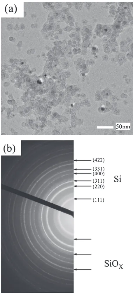
Figures 3(a) and 3(b) show a TEM image and ED patterns of Si clusters deposited on TEM grids with the electric power of 300 W and annealed at 670 K for 1.8©103s. In Fig. 3(a),
strong contrast regions are scarce and no void is observed because these Si clusters are coagulations of smaller primary Si particles.57) In Fig. 3(b), diffraction rings allotted to a
diamond-like Si phase are detected together with those to an amorphous like SiOXphase.23)
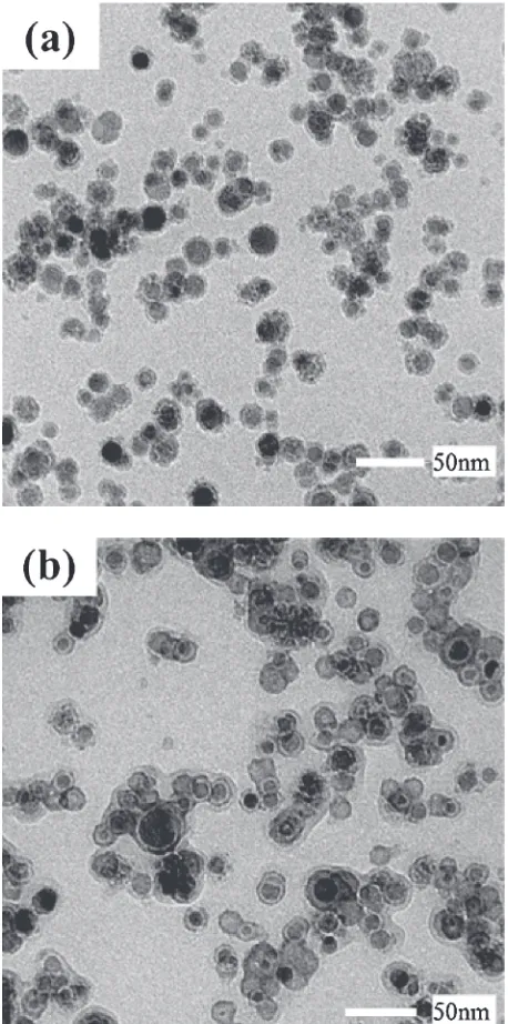
Figure 4 shows TEM images of FeSi core/Si shell clusters, whose average chemical composition is Fe 40 at%Si, prepared with 200 W without setting the partition plate: (a) as-prepared and (b) annealed at 670 K for 1.8© 103s. In the as-deposited state (Fig. 4(a)), double-layered (coreshell) clusters are predominant: dark contrast cores are surrounded by grey contrast shells. In the annealed state (Fig. 4(b)), on the other hand, the complex morphology is enhanced and multiply-layered clusters are observed. These features are attributed to heterogeneities in the structures, chemical compositions and degrees of oxidation among respective clusters. Moreover, cluster perimeters become more vague in Fig. 4(b) than in Fig. 4(a), being due to a contamination effect in the annealed specimen. In the ED patterns (see Figs. 5(a) and 5(b)) diffraction rings of a bcc phase are predominant and very weak diffraction rings of an Fe3O4or£-Fe2O3phase are detectable. The relative intensity
of the oxide to bcc phase is slightly increased by annealing, but the volume fraction of the retained bcc phase is much higher in the Fe/Si hybrid clusters than in the Fe clusters, implying that the Fe/Si hybrid clusters are not severely oxidized.
Figure 6 shows X-ray diffraction patterns of Fe/Si cluster hybrid, whose average chemical composition is Fe40 at%Si, prepared with the electric power of 200 W without setting the partition plate: (a) as-prepared and (b) annealed at 670 K
Fig. 1 Schemes of an improved double source plasma-gas-condensation system. (a) A top view of the system and (b) a side view of the sputtering room from the left hand side of Fig. 1(a).
[image:2.595.62.274.73.328.2]for 1.8©103s. In Fig. 6(a), the diffraction lines allotted to
a bcc phase are predominant and weak diffraction lines to an Fe3O4 or £-Fe2O3 phase are detectable, whereas a very
broad hill between 2030° is ascribed to the glass substrate. The diffraction lines of the bcc phase in Fig. 6(b) is clearer than those in Fig. 6(a), indicating that the crystal sizes are increased and crystalline qualities are improved after annealing. The lattice constant of the bcc phase is 0.283 nm for the as-deposited state and becomes 0.282 nm for the annealed state, roughly corresponding to the one for bulk Fe25 at%Si alloys.22)
Figures 7(a) and 7(b) show electrical resistivity, µ, as a function of temperature for assemblies of Fe clusters and Fe
Si core/Si shell clusters prepared with the electric power of 200 W, where the average chemical composition of the latter is Fe43 at%Si. In these experiments, the specimens were heated with the rate of 0.6 K/s from 300 to 670 K, kept at 670 K for 1.8©103s and cooled with the rate of 0.1 K/s. In the as-deposited Fe cluster assembly the µ value is so large as 1.5©10¹2³m because the packing density is about 30%of bulk Fe and these cluster surfaces are partly oxidized. With increasing temperature, the µvalue decreases between 300 and 500 K and slightly increases between 500 and 670 K. With decreasing temperature, it monotonically increases, revealing a marked hysteresis between the heating and cooling curves. In the FeSi core/Si shell hybrid clusters
Fig. 2 (a) A TEM image and (b) a selected area ED pattern of Fe clusters prepared using a single glow discharge source with an input electric power of 250 W and annealed at 670 K for 1.8©103s.
[image:3.595.311.539.68.571.2] [image:3.595.50.285.69.571.2]assembly, on the other hand, the µ value monotonically decreases with increasing temperature up to 670 K, then monotonically increases with decreasing temperature, indi-cating a semiconductor character. A hysteresis between the heating and cooling curves is marked at high temperatures, while the difference between the large resistivity values of the heating and cooling curves is apparently small at low temperatures.
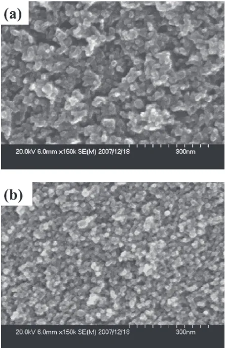
Figures 8(a) and 8(b) show the SEM images of Fe cluster and FeSi core/Si shell cluster assemblies observed after electrical resistivity measurements shown in Fig. 7. In Fig. 8(a) (the Fe cluster assembly), there are 2030 nm size clusters in contrast to the initial cluster sizes of about 16 nm by TEM observation, indicating the necking and coalescence of these clusters.2,24,25) For the FeSi core/Si shell cluster
Fig. 4 TEM images of Fe/Si cluster hybrids prepared using double glow discharge sources with the input electric powers of 200 W. (a) The as-prepared specimen (b) the same specimen after annealed at 670 K for 1.8©103s. The average composition is Fe40 at%Si.
Fig. 5 ED patterns of Fe/Si cluster hybrid heavily deposited on a TEM microgrid using double glow discharge sources with the input electric powers of 200 W. (a) The as-prepared specimen and (b) the same one after annealed at 670 K for 1.8©103s. The average composition is Fe
40 at%Si.
Fig. 6 X-ray diffraction patterns of Fe/Si cluster hybrid prepared using double glow discharge sources with the input electric powers of 200 W. (a) The as-prepared specimen and (b) the same one after annealed at 670 K for 1.8©103s. The average composition is Fe40 at%Si.
[image:4.595.55.284.70.531.2] [image:4.595.322.528.592.739.2]assembly, on the other hand, there are 1020 nm size clusters being consistent with the initial cluster size of 17 nm, indicating no marked coalescence.
4. Discussion
As described above, bcc disordered FeSi alloy cores are surrounded by amorphous Si shells in both the as-deposited and annealed Fe/Si cluster hybrids. Fe and Si atoms are mixed within the Fe-rich bcc phase field ranging the disordered primary solid solution (010 at%Si), the B2 type ordered phase (1011 at%Si) and the DO3 type ordered
phase (1125 at%Si) in the equilibrium phase diagram.18)Fe
atom diffusion is much faster and its activation energy is lower in the DO3type ordered Fe3Si alloys than in bcc Fe and
disordered Fe-rich FeSi alloys, while Si atom diffusion is slower and its activation energy is higher in the ordered alloys than in the disordered alloys26) because the high
vacancy concentrations are a consequence of the low vacancy formation energy of Fe atom sites in ordered Fe3Si alloys.
Indeed, DO3type ordered Fe3Si clusters have been grown via
a similar gas phase synthesis route where Fe and Si atoms from the Fe/Si composite target were mixed in one sputtering room.27) Such ordered Fe3Si alloy phase formation cannot
be excluded in the present Fe/Si hybrid clusters because the average lattice constant of bcc FeSi alloy phases is 0.282 nm in annealed Fe/Si hybrid clusters, being same as those of the as-prepared one and the DO3type ordered Fe3Si
phase in bulk FeSi alloys.22) However, no superstructure
line of the ordered Fe3Si phase was detected in the X-ray
diffraction pattern of annealed specimens, being attributable
to the severe chemical heterogeneity in these FeSi alloy cluster cores.
The B20-type ordered (¾-) FeSi phase, which is con-gruently stable up to the melting point of 1483 K and has a very large cohesive energy,1618)is not formed in the present Fe/Si hybrid clusters, too. When the amorphous FeSi layers on Si substrates were annealed or Fe thin films were deposited on a high temperature substrate, B20-type ordered FeSi alloy layers were formed at 570 K, and transformed to £-FeSi2 islands and ¢-FeSi2 rods at higher temperatures.28,29)
Anomalous metal-mediated crystallizations by low temper-ature annealing were also observed in amorphous semi-conductor/metal double-layered films, and ascribed to very fast grain boundary diffusion of Si (or Ge) atoms through metal layers.30,31)Since both Fe and Si diffusivities are small and their values for Fe are much smaller than that for Si in the bulk B20-type ordered FeSi alloy,32) the insufficient annealing procedures (the short period and low temperature) may hinder the growth of the ordered FeSi and FeSi2phases
in the present Fe/Si hybrid clusters.
Presumably the presence of Si shells is the most important factor to stabilize bcc FeSi alloy cores. In nanometer size clusters, the surface-to-volume ratio is so high that Si layers with the higher surface energy is maintained at the Fe/Si
Fig. 7 Electrical resistivity, µ, as a function of temperature for (a) Fe cluster and (b) Fe/Si hybrid cluster assemblies prepared using double glow discharge sources with the input electric powers of 200 W. The specimens were heated with the rate of 0.6 K/s from 300 to 670 K, kept at 670 K for 1.8©103s and cooled with the rate of 0.1 K/s. The average
composition is Fe43 at%Si.
Fig. 8 SEM images of Fe cluster and Fe/Si cluster hybrid assemblies prepared using double glow discharge sources with the input electric powers of 200 W and annealed at 670 K for 1.8©103s. (a) Fe cluster
[image:5.595.66.274.64.327.2] [image:5.595.313.541.70.422.2]hybrid cluster surfaces, i.e., a surface segregation effect. Then, the surface effect competes with the volume effect (forming abilities of ordered and intermetallic compound phases with high cohesive energies)1618) and stabilizes
disordered bcc FeSi alloy phases.33) Gradual oxidation of Si layers in the quartz glass tube suppress inward diffusion of Si atoms from Si shells to FeSi cores, leading to no Si-rich compound formation.6,11,12)
Metal surfaces are progressively oxidized in the following two stages. At first, oxygen molecules attach to the metal surface, form a thin oxide layer through which the electron tunnels and ionizes the oxygen molecules, and the electrical
field which is generated between the metal and surface of the oxide layer induces the outward diffusion of ionized metal atoms.34)After the oxide layer becomes thick, the metal
oxidation is dominated by thermal activation of ionized metal and oxygen atoms.1921)As shown in Fig. 2, voids and
hollows are formed in the central positions of oxidized Fe clusters with the average size of 10 nm annealed at 670 K for 1.8©103s. This is ascribed to the difference in diffusion speeds between metal and oxygen atoms through the oxide shell layers, i.e., Kirkendall effect.1921) As long as the outward diffusion of Fe atoms is much faster than the inward diffusion of O atoms through the oxidized shell layers formed on Fe cluster core surfaces, the excess vacancies are retained at the metal-core and oxide-shell interface. As oxidations are progressed, they form a void or a hollow at the core center to reduce the surface energies in Fe oxide clusters.
As shown in Fig. 3, Si clusters annealed at 670 K for 1.8©103s are not severely oxidized, and no void is formed
even though the chemical affinity of Si and O is rather high. This feature resembles to oxidation behaviors of Zn and Al islands deposited on TEM microgrids:35,36)no void is formed
in the large islands whose sizes are larger than 10 nm, while voids are observed in small ones whose sizes are less than 10 nm. In Zn and Al islands, the initial oxidation process is progressed very rapidly, while the thermal activation process is slowed down, i.e., self diffusions of ionized Zn and Al atoms through their oxide layers are too slow to grow their oxide layers. In particular, an amorphous or nanocrystalline oxide thin layers play a role of passive layers. Similarly SiOX
thin amorphous layers formed during the initial oxidation process interrupt further oxidation and void formation in Si clusters.
As shown in Fig. 4(b), complex morphology and multiply layered clusters are obtained in the annealed state of FeSi alloy cores/Si shell clusters, owing to chemical heterogene-ities in the Fe/Si hybrid clusters and different oxidation character of Fe and Si. No clear hollow are observed in the core centers of Fe/Si hybrid clusters though the unbalance between the fast outward diffusion of Fe atoms and slow inward diffusion of Si atoms is predictable to generate voids in the FeSi cores: the diffusion constants between 300 and 670 K extrapolated from the high temperature data are 10¹15 10¹12m2/s for Fe in Si, 10¹6010¹40m2/s for Si in Si, 10¹35 10¹23m2/s for Fe in Fe, 10¹3110¹23m2/s for Si in Fe.37)As
discussed in the above paragraph, the surfaces of Si shells are oxidized when the Fe/Si hybrid clusters are exposed to ambient atmosphere. Such SiOX thin layers are stable and
protect further oxidations of Si shells and FeSi cores. Since
SiOX do not form solid solution with Fe,1318) the heat
treatment slightly enhances Fe and Si atom diffusion in the FeSi cores. The marked drop of the contrast at around interfaces between FeSi cores and Si shells in Fig. 4(b) is presumably ascribed to the rapid density change, which is enhanced by the accumulation of voids and/or the progress of phase separation.
The temperature dependent characteristics of µshown in Fig. 7 reflect the difference in the oxidation behaviors and morphology changes between Fe cluster and Fe/Si hybrid cluster assemblies. For the Fe cluster assembly, the µvalue decreases with increasingTup to 500 K and increases withT for T>500 K, while it increases with decreasing T. These results are attributed to two phenomena: the decrease inµby coalescence of Fe clusters and the increase inµby oxidation. In the Fe/Si hybrid cluster assembly, the large µ value monotonically decreases with T up to 670 K where it originates from weakly contacted networks of semiconducting Si shells and metallic FeSi cores in the observed temperature range. Since the oxidation of FeSi cores is not so severe, the marked increase at around 670 K is attributed to the internal structure change in these clusters; i.e., void and/or hollow formations between FeSi cores and Si shells during the annealing at this temperature. With decreasingT,µ monotoni-cally increases and its value at 300 K is almost same between the as-prepared and annealed states. In the logarithmic scale
figure, the hysteresis of the µTcurve is emphasized at high temperature, while weakened at low temperature.
5. Summary
We observe TEM and X-ray diffraction of annealed Fe, Si and Fe/Si hybrid clusters, and temperature dependence of electrical resistivities for their assemblies, which have been prepared using the PGCCD systems with two glow discharge sources. In Fe clusters which are easily oxidized, the outward diffusion of Fe atoms is faster than the inward diffusion of O atoms, and the excess vacancies are accumulated to form voids in the central regions. In Si and clusters, where the surface oxidation is progressed very fast at the initial stage and decelerated by formation of stable surface oxide layers at the thermal activation stage, suppressing further oxidation and void formation in Si clusters. In Fe/Si cluster hybrids, since SiOXthin layers on Si shell surfaces are rather stable
and protect further oxidations of Si shells and FeSi cores. The diffusions of Fe and Si atoms in the core regions leave their vacancies, which are accumulated to become voids and/or hollows between FeSi cores and Si shell resulting in the complex morphology and multiply layered clusters.
Acknowledgment
The authors wish to thank Mrs. Y. Nakai for her assistance. This work was financially supported by Intellectual Cluster Project founded by the Ministry of Education, Culture, Sports, Science and Technology (MEXT), Japan, Aichi Prefecture, Nagoya City and Aichi Science and Technology Foundation, a Grant-in-Aid for Scientific Research (20246110) given by MEXT, Japan. It was also experimen-tally supported by the Nanotechnology Network Project
organized by MEXT, Japan. One of the authors (KS) appreciates the support from Nagoya Industrial Science Research Institute and Research Institute for Science and Technology of Tokyo Denki University, Japan (Grant No. 021224).
REFERENCES
1) R. P. Andres, R. S. Averback, W. L. Brown, L. E. Brus, W. A. Goddard, III, A. Kaldor, S. G. Louie, M. Moscovits, P. S. Peercy, S. J. Riley, R. W. Siegel, F. Spaepen and Y. Wang:J. Mater. Res.4(1989) 704736.
2) A. S. Edelstein and R. C. Cammarata, (ed.):Nanomaterials, Syntesis, Properties and Applications, (Institute of Physics, 1996).
3) H. Haberland, M. Karrais, M. Mall and Y. Thurner: J. Vac. Sci. Technol. A10(1992) 32663271.
4) K. Sumiyama, T. Hihara, D. L. Peng and S. Yamamuro:Encyclopedia of Nanoscience and Nanotechnology10, ed. by H. S. Nalwa (American Scientific Publishers, 2004) pp. 471507.
5) R. Katoh, T. Hihara, D. L. Peng and K. Sumiyama:Appl. Phys. Lett.82
(2003) 26882690.
6) R. Katoh, T. Hihara, D. L. Peng and K. Sumiyama:Appl. Phys. Lett.87
(2005) 252501.
7) R. Katoh, T. Hihara, D. L. Peng and K. Sumiyama:J. Appl. Phys.100
(2006) 034308.
8) R. Katoh, K. Nonaka, K. Sumiyama, D. L. Peng and T. Hihara:Mater. Trans.49(2008) 18301835.
9) A. Monden, R. Katoh, K. Sumiyama and D. L. Peng:Mater. Trans.47
(2006) 19491952.
10) K. Sumiyama, A. Monden, R. Katoh, N. Tanaka, D. L. Peng and T. Hihara:Mater. Trans.50(2009) 516522.
11) K. Sumiyama, R. Katoh, S. Kadowaki and T. Hihara:J. Nanopart. Res.
12(2010) 25892596.
12) N. Tanaka, K. Sumiyama, R. Katoh, T. Hihara, K. Sato, T. J. Konno and K. Mibu:Mater. Trans.51(2010) 19901996.
13) A. F. Wells (ed.): Structural Inorganic Chemistry, 5th edition, (Clarendon Press, Oxford, 1987) p. 551.
14) A. F. Wells (ed.): Structural Inorganic Chemistry, 5th edition, (Clarendon Press, Oxford, 1987) p. 982.
15) A. F. Wells (ed.): Structural Inorganic Chemistry, 5th edition,
(Clarendon Press, Oxford, 1987) p. 985.
16) F. R. de Boer, R. Boom, W. C. M. Mattens, A. R. Miedema and A. K. Niessen: Cohesion in Metals®Transition Metal Alloys, (North-Holland, Amsterdam, 1989) p. 231.
17) F. R. de Boer, R. Boom, W. C. M. Mattens, A. R. Miedema and A. K. Niessen: Cohesion in Metals®Transition Metal Alloys, (North-Holland, Amsterdam, 1989) pp. 662663.
18) T. B. Massalski, H. Okamoto, P. R. Subramanian and L. Kacprzak:
Binary Alloy Phase Diagrams, 2nd ed., (American Society of Metals, Metals Park, Ohio, 1990) pp. 17711772.
19) C. M. Wang, D. R. Baer, L. E. Thomas, J. E. Amonette, J. Antony, Y. Qiang and G. Duscher:J. Appl. Phys.98(2005) 094308.
20) R. Nakamura, D. Tokozakura, J.-G. Lee, H. Mori and H. Nakajima:
Materia Japan47(2008) 368374.
21) Y. Yin, R. M. Rioux, C. K. Erdonmez, S. Hughes, G. A. Somorjai and A. P. Alvisatos:Science304(2004) 711714.
22) W. B. Pearson: A Handbook of Lattice Spacings and Structures of Metals and Alloys, (Pergamon Press, New York, 1958) p. 638. 23) G. M. Kurdyumov, V. A. Molocheko and A. V. Chekunov: Inorg.
Mater.2(1966) 1539.
24) S. Sugano and H. Koizumi:Microcluster Physics, 2nd ed., (Springer-Verlag, Berlin, 1998).
25) P. Jensen:Rev. Mod. Phys.71(1999) 16951735.
26) A. Gude and H. Mehrer:Phil. Mag. A76(1997) 129.
27) Y. Jing, Y. H. Xu and J. P. Wang:J. Appl. Phys.105(2009) 07B520.
28) J. H. Won, A. Kovács, M. Naito, M. Ishimaru and Y. Hirotsu:J. Appl. Phys.102(2007) 103512.
29) J. H. Won, K. Sato, M. Ishimaru and Y. Hirotsu:J. Appl. Phys.100
(2006) 014307.
30) A. Hiraki:J. Electrochem. Soc.127(1980) 26622665.
31) F. Katsuki, K. Hanafusa, M. Yonemura, T. Koyama and M. Doi:
J. Appl. Phys.89(2001) 46434647.
32) M. Salamon and H. Mehrer:Phil. Mag. A79(1999) 21372155.
33) Y. H. Xu and J. P. Wang:Adv. Mat.20(2008) 994999.
34) N. Cabrera and N. F. Mott:Rep. Prog. Phys.12(1949) 163184.
35) R. Nakamura, J.-G. Lee, D. Tokozakura, H. Mori and H. Nakajima:
Mater. Lett.61(2007) 10601063.
36) R. Nakamura, D. Tokozakura, H. Nakajima, J.-G. Lee and H. Mori:
J. Appl. Phys.101(2007) 074303.