Printed Electronics from
Solution-Processed 2D Materials
a thesis presented by Adam G. Kelly
under the supervision of Professor Jonathan N. Coleman
for the degree of Doctor of Philosophy
in the subject of Physics
School of Physics, Trinity College Dublin
Declaration
I declare that this thesis has not been submitted as an exercise for a degree at this or any other university and it is entirely my own work.
I agree to deposit this thesis in the University’s open access institutional repository or allow the library to do so on my behalf, subject to Irish Copyright Legislation and Trinity College Library conditions of use and acknowledgement.
Elements of this work that have been carried out jointly with others or by collaborators have been duly acknowledged in the text wherever included.
Printed Electronics from Solution-Processed 2D Materials
Abstract
The fervour created in the wake of the graphene gold-rush has fuelled investigative momentum over the last decade. The maturity of liquid-phase processing has meant that solution-processed layered crystals can be now be consolidated with additive manufacturing and devices based on printed nanosheet networks are now regularly reported. There are many challenges associated with printed architecture and this work aims to address the some of the issues faced by the current generation of nanosheet-network devices.
As contemporary printed devices move from lateral to vertical geometry, it was first necessary to develop a methodology for printing continuous, pinhole-free films to prevent unwanted interlayer contact. This was undertaken through a capacitor study where the devices were printed through sequential deposition of conductive graphene and dielectric hexagonal boron nitride (h-BN) nanosheet networks. Such heterostructures will only function as capacitors once the dielectric layer is continuous and, through trial and error, the dielectric layers were found to be pinhole-free at thicknesses above 1.65 μm. Impedance spectroscopy showed that such heterostructures act as series combinations of a capacitor and a resistor, with the expected dimensional scaling of the capacitance. The areal capacitance ranged from 0.24 to 1.1 nF cm−2, with an average series resistance of 120 kΩ. The fitting of the Bode plots also provided an averageRCtime constant of 0.74 μs for these devices. This development thus paves the way toward more complex multilayer devices.
currents at relatively low drive voltages, in contrast with other devices of comparable mobility. An all-printed, vertically stacked transistor was then demonstrated with graphene source, drain, and gate electrodes, a WSe2 channel, and a BN separator—all formed from nanosheet networks. The BN network contains the electrolyte within its porous interior, which facilitates electrolytic gating in a solid-like structure. This proof-of-concept transistor performs reasonably well, with an on:off ratio of∼25 and a transconductance of 22 μS.
List of Publications
1. Kelly, A.G., Finn, D., Harvey, A., Hallam, T., & Coleman, J.N. (2016). All-printed capacitors from graphene-BN-graphene nanosheet heterostructures.*Applied Physics Letters, 109(2), 023107.
*Basis for Chapter 4
2. Backes, C., Higgins, T.M., Kelly, A.G., Boland, C., Harvey, A., Hanlon, D., & Coleman, J.N. (2016). Guidelines for exfoliation, characterization and processing of layered materials produced by liquid exfoliation. Chemistry of Materials, 29(1), 243-255.
3. Harvey, A., Boland, J.B.., Godwin, I., Kelly, A.G., Szydłowska, B.M., Murtaza, G., Thomas, A., Lewis, D.J., & Coleman, J.N. (2017). Exploring the versatility of liquid phase exfoliation: producing 2D nanosheets from talcum powder, cat litter and beach sand.2D Materials, 4(2), 025054.
4. Kelly, A.G., Hallam, T., Backes, C., Harvey, A., Esmaeily, A. S., Godwin, I., Coelho, J., Nicolosi, V., Lauth, J., Kulkani, A., Kinge, S., Siebbeles, L.,Duesberg, G., & Coleman, J.N. (2017). All-printed thin-film transistors from networks of liquid-exfoliated nanosheets.*Science, 356(6333), 69-73.
*Basis for Chapter 5
5. Kelly, A.G., Murphy, C., Vega-Mayoral, V., Harvey, A., Esmaeily, A.S., Hallam, T., McCloskey, D., & Coleman, J.N. (2017). Tuneable photoconductivity and mobility enhancement in printed MoS2/graphene composites.*2D Materials, 4(4), 041006.
*Basis for Chapter 6
6. Mondal, S., Dutta, K., Dutta, S., Jana, D., Kelly, A.G., & De, S. (2018). Efficient Flexible White-Light Photodetectors Based on BiFeO3 Nanoparticles. ACS Applied Nano Materials, 1(2), 625-631.
Acknowledgements
I would like to begin by thanking Johnny for providing me with the opportunity to work with such an amazing group. I began this PhD believing that undergrad shenanigans were over and it was time to grow up however, I felt this going out the window the fifth time The Pav was mentioned during my interview. Over the last four years, I have always left a meeting feeling better about terrible results and always appreciated the focus and clarity that Johnny could bring to frustrating research.
I want to thank Toby for mentoring me on all things electronic. When I started, he mentioned that each PhD comes with about €20k worth of breakage so, in my last month, I think I’ll take out my underspend on the Temescal. Thanks to Claudia, a patient fountain of knowledge on everything nano and for providing proper etiquette on the consumption of lab wine. A big thanks to Tom, for providing the central question of this thesis and for having no qualms about going to the pub at 11 am on the only sunny day of the year. Umar, the scientific equivalent of MacGyver from whom I learned the fine art of brute force experimentation—there is no exact science in preliminary investigation. I started my PhD paired with Graeme who taught me a bunch of things he found useful including, but not limited to, Fibbers on a Sunday. To Seb, Conor, and Dan in the office, you may brighten up five days of the week but I still feel blameless over us being told to stop using the upstairs toilet. To the rest of the group; JB, Andrew, Sonia, Aideen, Dave, Cian, Ruiyuan and Victor, I’m deeply grateful for being able to share the last four years with you. To Yash and Domhnall, you’ve landed on your feet with these guys. A big thanks as well to Niall and all in the ASIN group for providing me with relentless access to their labs and equipment.
To all my friends outside of Trinity, I’m pretty sure the last four years count as attempted murder on your behalf but I wouldn’t change a single pint with you degenerates.
To Kejt, thank you for putting up with me over the past few years and, since I couldn’t have done this without you by my side, I’ll say this; te słowa są po polsku.
Finally, the biggest thanks of all to my family for the various types of support over the last 8 years. The ups and downs would have been unnavigable and this thesis would have been unachievable without you.
Contents
1 Introduction 1
2 2D Materials and their Synthesis 5
2.1 The Electronic Characteristics of the 2D Family . . . 7
2.1.1 Semi-metals . . . 7
2.1.2 Semiconductors . . . 11
2.1.3 Insulators . . . 16
2.2 Synthesis . . . 19
2.2.1 Solution Processing of 2D Materials . . . 21
2.2.2 Liquid-Phase Exfoliation . . . 23
3 Deposition and Applications 34 3.1 Printing Technologies . . . 36
3.1.1 Inkjet Printing . . . 36
3.1.2 Spray Coating . . . 44
3.2 The Nature of Printed Networks . . . 47
3.3 Electronic Devices . . . 51
3.3.1 Capacitors . . . 51
3.3.2 Photodetectors . . . 54
3.3.3 Transistors . . . 58
3.4 The Field of Printed Electronics . . . 66
4 Insulating the Vertical Layers 72 4.1 Experimental Procedure . . . 74
4.2 Results and Discussion . . . 76
4.2.1 Material Analysis . . . 76
4.2.2 Capacitor Overview . . . 79
4.2.3 Impedance Spectra . . . 81
4.3 Conclusions . . . 85
4.4 Coda . . . 86
5 Current Modulation in 2D Networks 88 5.1 Experimental Procedure . . . 90
5.2 Results and Discussion . . . 93
5.2.1 Material Analysis . . . 93
5.2.2 Electrical Characterisation . . . 97
5.2.3 Electrochemical Characterisation . . . 101
5.2.4 Transport Characterisation . . . 103
5.2.5 Temporal Behaviour . . . 107
5.2.6 All Printed Thin-Film Transistor . . . 111
5.3 Conclusions . . . 113
5.4 Coda . . . 114
6 Improving the Network Mobility 116 6.1 Experimental Procedure . . . 118
6.2 Results and Discussion . . . 119
6.2.1 Material and Device Analysis . . . 119
6.2.2 Carrier Transport and Electrical Characterisation . . . 122
6.2.3 Percolation Analysis . . . 126
6.3 Conclusions . . . 135
6.4 Coda . . . 135
7 Conclusions and Future Work 137 Appendix A Ancillary Techniques 144 A.1 Spectroscopic Characterisation . . . 145
A.2 Microscopic Characterisation . . . 150
Appendix B Derivations 157 B.1 Current Behaviour in a Field-Effect Transistor . . . 157
B.2 Mass- and Volume-Fraction Relationships in Percolating Networks . . . 163
List of Figures
2.1 Graphene . . . 9
2.2 Transition Metal Dichalcogenides . . . 12
2.3 TMD Band Structures . . . 14
2.4 Bandgap Transition with Layer Number . . . 15
2.5 Boron Nitride . . . 18
2.6 Liquid-Phase Exfoliation . . . 24
2.7 Dispersibility Curve . . . 29
2.8 Liquid Cascade Centrifugation . . . 32
3.1 Inkjet Printhead Schematics . . . 38
3.2 Range of Printable Fluid . . . 40
3.3 Printing Artefacts . . . 42
3.4 Airbrush Schematics . . . 45
3.5 The Nature of Printed Films . . . 48
3.6 Capacitors . . . 52
3.7 Photodetectors . . . 56
3.8 Transistors . . . 59
3.9 EDLs and Ionic Liquids . . . 64
4.1 Graphene and BN TEM Images . . . 76
4.2 Inks, TEM, and Spectroscopy . . . 78
4.3 Capacitor Schematics with SEM . . . 80
4.4 Impedance Spectra . . . 81
4.5 Frequency-Dependent Permittivity . . . 82
4.6 Dimensional Scaling of Capacitance . . . 84
5.1 Inks and TEM Images . . . 94
5.2 TMD Material Analysis . . . 95
5.4 Electrical Characterisation . . . 98
5.5 On:Off Ratios and Threshold Voltages . . . 100
5.6 Electrochemical Analysis . . . 101
5.7 Transport Analysis . . . 104
5.8 Summary of TMD Network Characteristics . . . 106
5.9 Temporal Response for Various Configurations . . . 108
5.10 A Fully Printed Nanosheet-Network Transistor . . . 112
6.1 Graphene and MoS2Inks . . . 119
6.2 Imagery of a Composite Photodetector . . . 120
6.3 Raman Spectroscopy of MoS2-Graphene Composites . . . 122
6.4 Conduction in MoS2-Graphene Composites. . . 124
6.5 Illuminated Response . . . 125
6.6 Percolation Scaling of Dark Conductivity . . . 128
6.7 Percolation Scaling of Photoconductivity . . . 130
6.8 Percolation Scaling of the Fractional Photoconductivity . . . 134
A.1 Cary UV-Vis Spectrophotometer . . . 146
A.2 Various Raman Processes . . . 149
A.3 AFM Schematic . . . 151
A.4 TEM Schematic . . . 153
A.5 SEM Schematic . . . 155
To my family and friends,
A recurrent theme that luck plays a large role in every
story of success; it almost always easy to identify a small
change in the story that would have turned a remarkable
achievement into a mediocre outcome.
Daniel Kahneman
1
Introduction
T
he frenetic pace of change in the 20thcentury has caused some of thelargest paradigm shifts seen by this age of human civilisation. In the span of a
lifetime, we have gone from the first manned flight to a manned space station,
from hardback encyclopaedias to instantaneous access to the entire human archive, and from
rapidly accelerating and this acceleration maps extremely well to the emergence of the field of
nanoscience and, in particular, of 2D materials.
Nanoscience is the umbrella term covering both the materials and their technology and
has tendrils extending back thousands of years—complexity is ever built on the shoulders of
giants. The fields of nanoscience, chemistry, material science, and many fields of engineering
have a common ancestor in early metallurgy as various nanomaterials were commonplace
during classical antiquity. Swords forged from Damascus steel were fortified with carbon
nanotubes, Mesopotamian pottery and Egyptian glassware contained colloidal nanoparticles
to create iridescent patterns, and clays have long been used by indigenous tribes as medicinal,
digestive, and cosmetic aids.1
The synthesis of fullerenes and carbon nanotubes consolidated nanoscience with material
science during the 90s but it was the isolation of graphene from a graphite crystal that drove
the hype that culminated in the Nobel Prize in 2010. This has catalysed investigation to the
point where nanoscience publications now comprise > 5% of all scientific publications and,
for better or worse, the number of nanoscience journals now numbers over 300. There has
been so much certainty over the potential of these materials that an offhand comment by a
colleague has become the central question of this thesis:
“What if it turns out that 2D materials are just shit?”
This was personally startling but requires consideration given the youth of the field. The
development of silicon-based electronics has built the world around us and it is extremely
unlikely that 2D materials will be able to compete in the near- to mid-term but this is far
from the only route to application.2 The Internet of Things means we are likely to see
semi-disposable devices. This brings many challenges which could potentially be addressed
through the emergence of additive manufacturing and, in particular, its subfield of printed
electronics. Printed electronics are currently based on organic polymers and this technology
has now commercially matured. However, the performance of these materials is intrinsically
limited which means that a research space is available where 2D materials may be able to
compete within in the near future. Beyond this, the growing demand to power our world
would be greatly served through the energy generation and storage capabilities of these
materials. Thus, the field, and this thesis, are currently striving to answer the above question
and to hopefully fulfil the potential of the nanoscale platform.
With this in mind, the aim of this work is to take steps towards addressing a prevailing
challenge; effective current modulation in a semiconducting 2D network. While current
modulation was shown in a printed graphene network in 2012, it is critical to demonstrate
the same with a semiconductor, but progress here has been limited. This points to the
complexity of the problem as many material, ink, and device issues must be resolved. One
such issue concerns the nature of printed 2D networks; as they are composed of discrete
particles, the networks are prone to discontinuities, or pinholes. This is a major issue as the
device architecture pivots from planar to vertical and a protocol for vertical layering is thus
presented in Chapter 4. This is developed through a printed capacitor study as device
functionality can only be achieved once the dielectric film is continuous.
The slow progress on printed transistors can be partially attributed to the gating method.
A thick 2D network will shunt a gate field meaning current modulation is confined to a
relatively thin layer of material at the oxide interface. It it much more effective to use a
then be gated. The liquid electrolyte creates an enormous device capacitance which allows
large currents to be driven despite the long device channels. Chapter 5 presents a method for
electrolytically gating a printed 2D network and four semiconducting materials are
characterised in this manner. This, integrated with the work in Chapter 4, then facilitates
the demonstration of a fully printed, 2D-network transistor.
As the mobility of these devices is relatively low, much future work will focus on raising
the network mobility to that of its individual constituents. A simple way to achieve this
could be through a conductor/semiconductor composite where the conductive
components are only present below the percolation threshold. Chapter 6 investigates the
viability of this proposal through a percolation study of printed photodetectors with
various graphene loadings blended into an MoS2network.
This thesis will conclude by reviewing the main findings and suggesting a direction for
future investigations. It is hoped that the work presented herein will add value to the
existing literature and facilitate further development of printed 2D electronics.
*A small note on this thesis; to preserve the flow of the narrative, the traditional Methods
and Characterisation section containing descriptions of the scientific machinery has been
distributed throughout the text. The techniques fundamental to the generation of 2D
materials and their deposition are described in the introductory chapters with the secondary
characterisation techniques described in Appendix A. On nomenclature; the termgraphene
A scientist looking at non-scientific problems just
dumb the next guy.
Richard Feynman
2
2D Materials and their Synthesis
T
he class of materials known as layered crystals has been the focusof an enormous amount of research since the field’s renaissance in 2004. While
1D nanomaterials such as carbon nanotubes have been heavily investigated since
the 1980s, it was not until the unambiguous demonstration of a free-standing graphene
contemporary terms, are those in which wavefunctions experience quantum confinement
in a single dimension meaning an electron gas is free to move in an ‘infinite’ 2D plane.
These planes, when stacked upon one another, form a layered crystal characterised by strong
covalent bonding within the layer and weak van der Waals bonding between the layers. It is
this weak interlayer bonding that allows discrete layers to be exfoliated from the bulk crystal
to create free-standing monolayers. This characteristic is perhaps most commonly seen in
pencilled text as the graphite crystal is shorn from pencil to page. When so isolated, the
discrete monolayers show vastly different properties from their bulk form and it is these
monolayer properties to which the word ‘exciting’ is romantically ascribed.
Despite the global abundance of various layered crystals, the synthesis of exfoliated 2D
materials in practical quantities has been far from trivial. The seminal graphene paper used
adhesive tape to peel nanosheets from bulk crystals and this remains an excellent method for
producing high quality flakes. However, the extreme tedium and low throughput make it
impractical and thoroughly incompatible with scalable manufacturing. This generally
applies to bottom-up synthesis where bulk crystals are grown from an elemental precursor.
A research space was thus available where existing solution processing strategies could be
adapted to exfoliate large amounts of material in liquids. The liquid environment offers
many advantages as dispersed media can easily be chemically modified, sorted by mass,
formed into composites, and, importantly, refined into inks for deposition with a variety of
established techniques. This chapter will begin by describing the characteristics of the
materials, with a focus on electronic properties, and then move on to describe how layered
2.1 The Electronic Characteristics of the 2D Family
Graphene is the face that launched a thousand grant proposals but the scope of
investigation has encompassed the entire class of layered crystals in recent years. Within the
family of layered materials, there is much diversity across crystal structure and stoichiometry
leading to a variety of commensurate properties such as electrical conductors and
semiconductors, dielectrics, ferromagnetics, catalysts, and thermoelectrics. Transition metal
dichalcogenides (TMDs), transition metal oxides (TMOs), 2D compounds such as boron
nitride, and single-element 2D structures such as arsenene have all featured in the literature
with increasing regularity over the past decade. Such versatility across the electronic
properties makes 2D materials extremely attractive for electronic applications. Within the
TMDs, for example, the coordination and oxidation of the metal atoms determine whether
the material will be metallic, semi-metallic, or semiconducting. This has generated much
excitement as each part of an electronic device, such as the electrodes or active channel, can
be constructed using a network solely composed of 2D materials.
2.1.1 Semi-metals
The story of graphene contains at its heart the power of the scientific framework, where
long-standing acceptance is upended by new discovery. Beginning in the 1930s, theoretical
analyses of layered crystals argued that a monolayer could not exist in isolation due to
thermodynamic instability. The monolayer was modelled as a completely flat atomic sheet
and, under this condition, thermal vibrations create anomalously large atomic
monolayer, but this was far from an impediment to general investigation. In 1947, PR
Wallace calculated the band structure and linear dispersion relation of the monolayer limit
of graphite, noting its semi-metallicity where free electrons “are created at higher
temperatures by excitation to a band contiguous to the highest one which is normally
filled.”3 Despite the apparent impossibility of creating a free-standing monolayer, its
properties could still be probed as part of the parent graphite crystal and various
crystallographic features were experimentally confirmed using transmission electron
microscopy and x-ray diffraction.4It was in the infancy of carbon nanotube research that
the term ‘graphene’ was first used to describe a graphite monolayer but, partly due to the
newly discovered properties of carbon nanotubes, research into layered crystals had slowed.
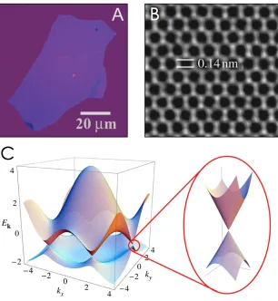
The field gained a second wind when Andre Geim and Konstantin Novoselov definitively
isolated a monolayer of graphene (shown in Figure 2.1A) and, more importantly, patterned
the samples with Hall bars to report the remarkable electronic properties.5 They also
reconciled the existential problem by showing that graphene is slightly corrugated rather
than completely flat which suppresses thermal vibrations and stabilises the monolayer.6
Graphene crystallises as a honeycomb lattice composed of sp2-hybridised carbon atoms,
shown in Figure 2.1B.7 Three electrons form deep valence bonds with the neighbouring
atoms leaving a remaining electron, corresponding to a non-hybridised p-state
perpendicular to the structure, to contribute to the conductivity of the system.8 The
strength of the hybridised sigma bonds makes the carbon atoms in the sheet extremely
robust against dislocation meaning crystallographic defects are rare in the basal plane. The
lack of lattice impurities means charge carriers can experience ballistic transport for
Figure 2.1:Graphene. A) AFM of the one of the first free-standing monolayers. Image from Ref. (5). B) A TEM image of the graphene la ce showing the 0.14 nm C-C bond length. Image from Ref. (7). C) The dispersion rela on of graphene. The linearity at the Dirac points is shown magnified. Image from Ref. (8).
Scattering artefacts pose a significant problem as ultra-thin crystals are particularly sensitive
to features such as dielectric mismatch which can significantly alter the Coulomb potential,
surface roughness which affects mobility through a sixth power law, and nanosheet edges
which can induce long-range Coulomb scattering.9
The ease in carrier transport across the basal plane is also due to to the non-negligible
extended states spanning over multiple in-plane sites.8 This does not apply to vertical
transport through the crystal however, as research into graphite has revealed over a
thousand-fold anisotropy between in-plane and out-of-plane conductivity.10This is due to
the interlayer van der Waals bond acting as a tunnelling barrier rather than an anisotropy in
the effective mass and is a feature common to all layered crystals.
Graphene’s semi-metallicity arises from the structure of its electronic bands at the vertices
of the hexagonal lattice, shown in Figure 2.1C. For small excitations at these vertices, known
as Dirac points, the dispersion relation is linear (shown expanded in Figure 2.1C). A
consequence of a linear dispersion relation is a zero effective electron mass and the Dirac
nomenclature is not simply an honorific but refers to the similarity in physical description
to quantum electrodynamics (QED) for massless fermions.6This means that QED effects
can present on a graphene sheet, albeit scaled by c/300.8These features confer an enormous
in-plane mobility; the seminal graphene paper reported a mobility of∼10,000 cm2V−1 s−1
and, using clever screening techniques, values are now often reported > 250,000 cm2V−1s−1
(cf. silicon∼3000 cm2V−1s−1).11
The wealth of publications during the graphene gold-rush strove to find where graphene
would be best suited in the short term. In Geim and Novoselov’s follow up paper in 2007,6
they point out
Despite the reigning optimism about graphene-based electronics,
‘graphenium’ microprocessors are unlikely to appear for the next 20 years. In
the meantime, many other graphene-based applications are likely to come of
age. In this respect, clear parallels with nanotubes allow a highly educated
This prediction has been mostly fulfilled as commercial graphene applications are
composite-based and polymers can be rendered conductive at less than 2% loading.12In the
much broader field of device prototyping, ease of synthesis and the wealth of global
experience has meant graphene is frequently used as an electrical conductor in 2D
electronics.
2.1.2 Semiconductors
The discovery of a stable monolayer of graphene was in many ways the keys to the kingdom.
It was immediately obvious that other layered crystals could be exfoliated in a similar
manner and a range of stable monolayers were published the following year.13Among these
was molybdenum disulphide (MoS2), an inorganic layered compound first studied in the
1920s.14 MoS
2 belongs to a subclass of layered crystals called transition metal
dichalcogenides (TMDs) which, like graphite, show an exceptional set of properties as the
crystal is scaled down to the monolayer.
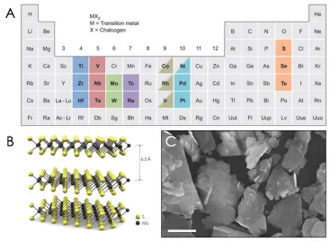
TMDs crystallise in a generalised MX2 stoichiometry, where M refers to a transition
metal and X refers to a chalcogen of sulphur, selenium, or tellurium. Forty combinations of
the elements highlighted in Figure 2.2A form layered crystals, each of which has a unique
chemistry and band structure; from insulators such as HfS2, semiconductors such as MoS2
and WS2, semi-metals such as WTe2 and TiSe2, to metals such as NbS2 and VSe2.15While
graphene is formed of a single plane of carbon atoms, a TMD monolayer consists of a
hexagonal plane of transition metal atoms contained between two offset hexagonal planes
of chalcogen atoms in the form X-M-X (Figure 2.2B). This monolayer structure is∼0.7 nm
Figure 2.2:Transi on metal dichalcogenides. A) Table of TMD elements. Image from Ref. (15). B) Schema c of a TMD crystal. Image from Ref. (16). C) An SEM image of MoS2bulk powder.
crystal. The bulk crystals themselves are typically a messy affair (Figure 2.2C) as they are
composed of a broad distribution of monolayer lengths—far from the uniformity depicted
in adjacent rendering.
Although all layered TMDs are composed of hexagonal planes, the X-M-X structure is
not isomorphic across the various metals and chalcogens; a thermodynamically-preferable
unit cell depends on the metal and chalcogen bonds leading to a variety of polymorphs.
Further, each layer in a bulk crystal can be stacked in a number of different sequences
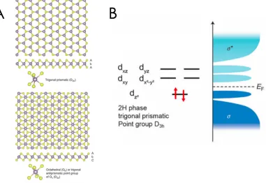
leading to a variety of polytyp . The most common polymorphs are 1T (trigonal), 2H
(hexagonal), and 3R (rhombohedral). Here, the integer refers to the number of monolayers
polytypes. The 2H polymorph of MoS2, for example, can be stacked in three different
polytypes. Monolayer TMDs show only two polymorphs—trigonal prismatic and
octahedral, shown in Figure 2.3A. MoS2 is most commonly found in the semiconducting
2H phase with AbA BaB stacking (Figure 2.3A) but a metallic 1T phase with AbC AbC
stacking can be induced at certain pressures and temperatures.17
Moving from Group IV to Group X across the transition metals corresponds to a filling
of thed-states, and it is thed-electron count that gives rise to the electronic diversity. Deep
covalent bonding between the metal and chalcogens- andp-states results in bonding (σ) and
anti-bonding (σ*) bands (Figure 2.3B) and contained between these are thed-bands whose
filling produces the semiconducting, metallic, or insulating behaviour.15When thed-bands
are partially filled, the TMD (such as 2H-NbSe2and 1T-ReS2) exhibits metallic conductivity.
The 2H phase of Group VI TMDs, such as MoS2and WS2, has a filleddz-band leaving the
Fermi level located between bands (Figure 2.3B) resulting in semiconducting behaviour.18
The band structures of the Group VI TMDs have now been heavily reported, typically
using MoS2 as a model system for the other Group VI compounds. Despite being
isoelectronic, the tungsten-based compounds contain higher energy band structures
compared to their molybdenum analogues due to the higher energy of filled 5d-state
compared to the 4d-state.19The semiconducting Group VI TMDs are of particular interest
not simply because of their abundance, in terms of both physical material and in the
academic literature, but because of their distinct transition in electronic behaviour as the
crystal is exfoliated down to the monolayer. The band structure at the Γ point of the
Brillouin zone of MoS2 contains a considerable contribution from chalcogenpz-states that
Figure 2.3:TMD band structures. A) TMD la ce structures with two different polymorphs. Image from Ref. (15). B) The band filling of Group VI TMDs. Image from Ref. (18).
has the effect of depressing the valence band maximum and raising the conduction band
minimum.20This bandgap-widening is shown for MoS2in Figure 2.4 where the bulk gap of
∼1.2 eV widens to∼1.8 eV in monolayer and this 50% increase is generally the case for other
Group VI compounds.15 Perhaps the most striking difference between the bulk and
monolayer band structures is the transition of the bandgap from indirect to direct. With
decreasing layer number, the indirect bandgap shifts upwards by ∼ 0.6 eV causing a
crossover to a direct-gap material in the monolayer limit and the enhancement in
photoluminescence is extreme; the luminescent quantum efficiency has been reported to
increase by 104.21The direct bandgaps of the Group VI monolayers are also well matched to
Figure 2.4:Bandgap transi on with layer number. The bandgap transi on from indirect to direct as the crystal is exfoliated down to the monolayer. Image from Ref. (15).
applications.22,23,24
The chalcogen atoms that terminate the surface layers are absent of dangling bonds which
confers good ambient stability but this does not imply a high electronic quality. The most
commonly reported material defects are chalcogen vacancies and anti-site substitutions (an
S atom replaced by a Mo atom in MoS2, for example) and the native n-type behaviour seen
in MoS2 has been attributed to donor states arising from such chalcogen vacancies.25 The
effect of vacancy density on charge transport is significant and this random crystallographic
disruption is the suggested cause of the discrepancy in the mobility values across seemingly
identical devices.26Furthermore, the electrical properties of Group VI devices are also known
to be highly sensitive to extrinsic effects arising from surfaces and interfaces such as metal
The mobility of TMDs is modest compared to graphene in part due to the high vacancy
density but also a far higher effective charge carrier mass. In particular, it is the intrinsic
energy bandgap that has ensured that semiconducting TMDs have featured prominently in
the device literature over the past decade. The mobility extracted from mono- to few-layer
Group VI TMDs is on the order of several hundred cm2 V−1 s−1 with the higher values
coming from heavily engineered devices.27,28,29Daset al. appear to hold the state-of-the-art
mobility of ∼ 700 cm2 V−1 s−1 with a back-gated MoS
2 transistor and an atomic-layer
deposited Al2O3dielectric.30Such benchmark devices are hardly made in a scalable manner
(yet) however there is clear value in finding the performance ceiling as the characterisation
of TMD electronics is still in its infancy.
2.1.3 Insulators
While much of the focus of investigation has been on characterising and modulating
current flow through the 2D materials, it is of critical importance to have non-conductive
regions within the electronic architecture. There are a large variety of insulating materials
available within the family of layered crystals, from everyday products such as talcum
powder and cat litter,31 to synthetically produced boron nitride (BN). It was long believed
that BN did not occur naturally as elemental boron did not form any part of an essential
mineral until the discovery of a rock fragment containing the cubic form of BN in southern
Tibet in 2009.32 The lack of natural occurrence did not preclude lab synthesis however and
the layered, hexagonal form of BN, h-BN, has been used in cosmetics since at least the
1940s.33
properties leading to much of the same physical behaviour such as large thermal
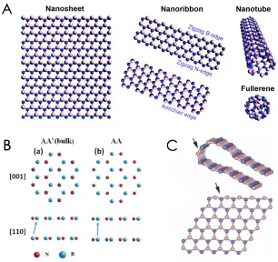
conductivity, chemical stability, and robust mechanical properties.34 Like graphite, a
monolayer of h-BN can be shaped into a range of nanoscale dimensionalities, each with
their own physical and electronic properties (Figure 2.5A). The first nanoscale investigation
of the h-BN lattice was in the form of nanotubes35and, shortly after the seminal graphene
paper, the bulk crystal was soon exfoliated into a free-standing monolayer.13
Like graphene, the h-BN monolayer is characterised by deep in-plane sigma bonds
formed by hybridisation of the 2s-, 2px-, and 2py-states leaving the non-hybridised
out-of-plane 2pz-state to weakly interact with adjacent layers. While these bonds are purely
covalent in graphene, electrons are transferred from the boron to the nitrogen sites due to
their difference in electronegativity.36 This charge transfer is an important difference as it
brings an ionic character to the bonds but also opens up a wide bandgap in the electronic
structure. Despite much study on the subject, the nature of the h-BN bandgap remained
elusive as ab initio calculations, predicting an indirect bandgap, could not be reconciled
with optical experiments which indicated a direct gap. This was only resolved in 2016 by Gil
et al.who conclusively demonstrated an indirect bandgap at 5.955 eV.37
The discrepancy in reporting on the h-BN bandgap goes beyond merely direct/indirect as
values for the gap itself typically range from 5.5–6 eV.38 The reason for this lies in the
variance of stacking orders which is influenced by the ionic bonds within the basal plane
(Figure 2.5B). Compared to graphene, the energetic landscape of a h-BN basal plane is
heavily corrugated due to the non-uniform distribution of charge across the atomic sites.36
In a bulk h-BN crystal, the van der Waals interaction will fix the interlayer distance at 0.33
Figure 2.5:Boron nitride. A) The various structures that can be formed from a boron nitride nanosheet. Image from Ref. (33). B) The stacking arrangements that can lead to the varia on in observed bandgap. C) The forma on of an interlayer bond, or lip-lip interac on. Image from Ref. (33).
governed by the ionic landscape of their basal planes. As one layer is translated across
another—at the fixed distance—the bandgap can vary by up to 0.6 eV.39
Another effect of the ionic bond is the formation of interlayer chemical bonds,
something relatively infrequent with the C-C bonds in graphene. It has been shown that
zigzag edges of two h-BN monolayers can bond (a “lip-lip” interaction) resulting in a
structure akin to a folded-over monolayer (Figure 2.5C). By decreasing the number of edge
sites, the conjoined bilayer reaches an energy minimum and greater structural stability.40It
or N-N, instead of a lower energy B-N) which leads to more pristine basal planes.38 The
anchoring of monolayers through these lip-lip interactions may also contribute to the
frustratingly low abundance of monolayer h-BN generated from top-down synthesis.
h-BN has seen its greatest value when used in conjunction with other 2D materials as an
atomically-flat dielectric interface has been vital in setting benchmarks. The absence of
dangling bonds and surface charge traps has meant a graphene device shows a roughness
decrease of ∼ two orders of magnitude leading to enormous improvements in charge
transport compared to similar devices on SiO2.41 This has allowed heterostructures of
h-BN/graphene/h-BN to exhibit mobilities of∼500,000 cm2V−1s−1.42
2.2 Synthesis
Since 2004, the renewed interest in layered crystals has brought with it a commensurate
explosion of research into monolayer production. The superlative properties demonstrated
with 2D crystals relied on high quality, pristine samples that were peeled from a bulk crystal
using adhesive tape. While mechanical exfoliation creates extremely high quality
monolayers, it suffers from low yields and production rates. This may be suitable for proof
of concept but an abundance of synthesis strategies have been developed in the intervening
years as 2D materials grow from infancy to industry. These strategies can be broadly split
into either bottom-up or top-down, depending on how one generates the monolayer.
A comparison between emergent 2D materials and silicon-based technologies was
inevitable once the extent of the electronic properties became clear. The king’s ransom
invested in fabrication units by companies such as Intel and Samsung means industry has a
bottom-up strategies such as chemical vapour deposition (CVD) have shown great promise
for monolayer growth. CVD uses a high temperature furnace to react (or decompose) a
vapour-phase precursor with a metal powder or bare substrate. MoS2, for example, can be
grown by sulphurisation of evaporated metal films, although this lacks the finesse of
modern CVD.43 While early iterations of CVD-grown materials were heavily
polycrystalline, wafer-scale single-crystal growth has now been demonstrated for monolayer
graphene,44MoS
2,45and WS2.46It is clear that CVD approaches show potential for many high-end electronic applications, however its scalability may be limited by furnace sizes,
substrate area, and substrate material.47Other bottom-up methods such as epitaxial growth
and ALD suffer from similar drawbacks. Furthermore, bottom-up synthesis is simply not
an optimal approach for generating a sufficient amount of material for use in applications
such as polymer48 or glass49 composites or energy storage applications whose properties
scale with surface area.
The top-down approach to monolayer synthesis is generally referred to as exfoliation
where a layered crystal is processed into discrete nanosheets. The early TMD work in the
1960s was often performed on nanosheets that were peeled from the parent crystal using
adhesive tape.50 While mono- or few-layer nanosheets may have then been exfoliated, the
resolution of the available instrumentation was unable to definitively identify them until
the efforts of Geim et al. in 2004. The difficulty in processing monolayers created by
mechanical exfoliation is a major bottleneck in the production rate and, like the early days of
carbon nanotube (CNT) research, generating a large quantity of material posed a significant
challenge. This issue is present in both bottom-up and top-down synthesis but can be
2.2.1 Solution Processing of 2D Materials
The large amount of processing and analysis possible on liquid-dispersed media has made
solution processing particularly attractive for the 2D platform. Techniques such as optical
spectroscopy can probe samples containing billions of nanosheets to extract statistical
information about the ensemble51, liquid-dispersed nanosheets can be easily sorted by size
and thickness,52 and, in particular, liquid samples can be deposited using well-established
techniques such as inkjet printing,53spin coating,54or spray coating.55The delamination of
layered crystals in liquids can be broadly parsed into two classes; intercalation and
exfoliation.
Layered crystals have been processed in liquids since 1859 when, in the reckless abandon
of classical science, graphite oxide was first synthesised by intercalating graphite with heavily
concentrated acids and then exfoliating with aggressive oxidisers.56 A century later,
Hummers and Offeman developed a less fatal method using potassium permanganate and
sulphuric acid to add carboxyl (-COOH), hydroxyl (-OH), and epoxide (C-O-H) groups to
the basal planes.57Such chemical modification polarises the crystal rendering it hydrophilic.
This allows water molecules to be drawn between the layers to facilitate exfoliation upon
ultrasonication and stability is then provided by the basal plane functionalisation. Using
more modern and less hazardous methods, graphene oxide dispersions with high monolayer
content can now be produced with lateral basal plane lengths of up to 50 µm.58While it is
possible to remove the functional groups using wet chemical reduction to yield reduced
graphene oxide, the basal plane contains many vacancies and defects which disrupt the
defects and reseeding vacancies pose a significant challenge. This is a fundamental problem
for device physics but the high degree of tunability bestowed by functionalisation has been
embraced by chemists59 and the number of papers published on graphene oxide is now
rapidly increasing year on year.
A parent crystal can also be dilated by intercalating other molecules between the layers
and the class of intercalation compounds is now well reported.60The interlayer widening is
a function of intercalant diameter where a wider spacing imparts a lower net cost of
exfoliation. The use of intercalants such n-butyllithium can also transfer charge to the layer
which further reduces the interlayer binding energy.61 The dilated crystal can then be
exfoliated by ultrasonication or thermal shock and discrete nanosheets are stabilised against
reaggregation by surfactants or the transferred charge from the intercalants. As one can
imagine, charge transfer to the nanosheets renders their properties distinct from their
pristine counterparts and, in general, the nanosheets tend to be negatively charged.15This
drives a reaction with water, leading again to basal plane functionalisation in the case of
graphene but TMDs are not reported to react in a similar manner. Instead,
negatively-charged Group VI TMDs now have their d-states filled causing a
semiconducting-to-metallic transition.15 This places a substantial constraint on this
technique but, as with graphene oxide, much work continues on restoring the properties of
pristine nanosheets despite limited success. It is these limitations that created a space for a
2.2.2 Liquid-Phase Exfoliation
In a testament to the speed of progress, it was just four years after the mechanical exfoliation
of graphene that liquid-phase exfoliation (LPE) was developed for exfoliating layered
crystals.62 LPE is a simple method for overcoming the interlayer forces using ultrasonic or
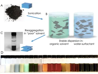
shear energy in a stabilising environment. The process proceeds as shown in Figure 2.6
where a bulk powder (Figure 2.6A) is sonicated and the resultant dispersion is stabilised
using solvent-particulate interactions or a stabiliser such as surfactant (Figure 2.6B). In the
case of a solvent with a surface energy dissimilar to the material, reaggregation will occur
(Figure 2.6C). Scalability is achieved through shear force mixing, a similar exfoliation
mechanism, where industrial-scale quantities of 2D materials can be generated.63
LPE builds on decades of chemical exfoliation research but, crucially, mono- and
few-layer nanosheets are created rather than simply nanoscale particles with bulk properties.
These nanosheets are typically defect-free and do not have molecules covalently linked to
the basal plane which makes this process especially attractive for electronic
applications.62,63,64 The technique itself is also extremely versatile; it appears the entire
family of layered crystals is exfoliable using LPE (Figure 2.6D) and a layered material has yet
to be found that cannot be exfoliated in this manner.31Furthermore, 2D dispersions can be
easily processed into inks,65pastes,66or multicomponent composites.12Post-sonication, the
dispersions are highly polydisperse with an extremely broad distribution of lateral sheet size
and thickness. This could be a fundamental issue as the bandgap is strongly layer-dependent
but centrifugal processing allows sorting by mass and therefore nanosheet dimensions.
Figure 2.6:Liquid-phase exfolia on. A) An as-bought bulk powder. B) A dispersion stabilised though solvent or surfactant interac ons. Image from Ref. (66). C) A poorly stabilised dispersion, resul ng in considerable reaggrega on. D) Various dispersed materials. Image from Ref. (67).
minimise the energetic difference between exfoliated and unexfoliated material which slows
reaggregation.67 The dispersion can also be stabilised through addition of surfactants or
polymers to the bulk powder prior to sonication. The use of such stabilisers allows
exfoliation to proceed in non-toxic solvents such as water which are clearly preferable to
solvents with a ten-page MSDS. Common ionic surfactants, such as sodium
dodecylbenzenesulfonate or sodium cholate, work by non-covalently adsorbing onto the
nanosheet surface and electrostatically repelling other dispersed nanosheets thus preventing
reaggregation. This allows high concentration dispersions to be stable for potentially
Polymer stabilisation works in a similar manner where the polymer chain non-covalently
adsorbs onto the nanosheet surface but rather than electrically repelling other nanosheets,
reaggregation is prevented by steric repulsion. This process is very well understood and the
modelling has shown good success in predicting stable combinations of nanosheets,
polymers, and solvents.69 The obvious drawback to using surfactants or polymers is their
removal. The non-covalent adsorption means these additives can be removed without
compromising the nanosheet crystallinity but the removal methods themselves tend to be
incomplete and deleterious. A film composed of a nanosheet-polymer composite may show
good mechanical properties but the polymer chains strongly affect the electrical
characteristics necessitating their removal. For example, polymers from the cellulose family
can be removed by annealing at temperatures > 300◦C70although this restricts the type of
substrate one can use and processing above∼50◦C has been shown to degrade monolayer
photoluminescence.* Similarly, films containing surfactant need to be washed causing
material loss and it is unclear how much may reside in the film’s free volume. For the
electronic applications contained within this work, we thus chose to stabilise our
dispersions using solvent interactions with the goal of minimising nanosheet
contamination.
Dispersion by Ultrasonication
Ultrasonic cleaning was first commercialised in the 1950s but the underlying mechanisms
were initially not understood. It was over a decade later that ultrasonication received wide
interest in the biological community when early SONAR technology was developed for
submarine warfare. Researchers noticed that testing was killing local marine life and, shortly
after, biologists began to concentrate their efforts on understanding the effect of acoustic
waves on microscale systems.71 Nowadays, ultrasonication is a particularly useful method
for exfoliating layered crystals as the necessary equipment is common to most labs. It can be
achieved using a sonic bath or ultrasonic probe and, during operation, requires little
attention.
Ultrasonication is the generation of high intensity acoustic waves from a mechanical
source with wave propagation proceeding through a range of phenomena such as
cavitation, radiation pressure, and acoustic streaming.72 Exfoliation driven by ultrasound
can be primarily attributed to the implosion of cavitation bubbles producing high tensile
and shear stresses along with liquid jets which cause both exfoliation and fragmentation of
the crystal.68 Bath sonication involves low intensity ultrasonic waves which set up standing
waves in a small tank. This means there are regions of constructive and destructive
interference throughout the tank and, along with damping caused by the sample container,
means reproducibility is poor. Probe (or tip) sonication is a much higher intensity process
where a region of intense ultrasonication is established directly under the probe. The
ultrasonic intensity is a strong function of probe distance73 which makes reproducibility
challenging but, as nanosheets can be characterised in aggregate, individual variation can be
statistically subsumed.
Ultrasonication is a mechanically aggressive technique but does not appear to cause basal
plane damage as reporting indicates that the exfoliated nanosheets are quite pristine.63,64,74
During early work on graphene, a D-band appeared in the Raman spectra but its intensity
the nanosheet edges.64This was confirmed by demonstrating that the ratio of Raman D- to
G-bands scaled with the nanosheet edge-to-area ratio.75There has been much further Raman
analysis performed on LPE nanosheets and, while damage may occur for longer sonication
times, the crystals appear defect free.53,76,77However, Backeset al.68note “one complication is
that, as the structural quality of the product will depend on the actual quality of the starting
crystal, some researchers observe basal plane defects while others do not.”
Solvent Stabilisation
It is not enough to merely overcome the van der Waals interaction to successfully exfoliate
a crystal as the nanosheets will reaggregate unless stably dispersed. An effective solvent will
not only stabilise the exfoliated nanosheets but will also reduce the net energy required to
exfoliate the crystal.78This was first demonstrated for CNTs in 2008 by Berginet al. where
their early modelling showed that a successful solvent is one with a surface energy close to
that of the nanotubes and this was experimentally confirmed for N-methyl-2-pyrrolidone
(NMP) and dimethylformanide (DMF).79 These data suggested that graphite, and indeed
graphene, may be stable in such solvents as its surface energy is close to that of CNTs and this
was conclusively shown to be the case for NMP later in 2008.62A more expansive solvent
study found that those with surface energies close to 70 mJ m−2 produced relatively high
concentrations of dispersed material, shown in Figure 2.7, but tended to be have high boiling
points concurrent with high toxicity.80Here we can also see that common non-toxic solvents
such as water and isopropanol were found to lie outside the range although IPA still showed
some dispersibility indicating the understanding was incomplete.
a useful solvent but some were found to be weakly dispersive despite a closely matched
surface energy.80This was interpreted through deeper modelling with the Hildebrand and
Hansen solubility parameters from solubility theory. In solvent-solute systems,
intermolecular interactions can be divided into dispersive (D), polar (P), and
hydrogen-bonding (H) components. The Hildebrand parameter,δT, is the commonly used
form of the cohesive energy density,EC,T/V, whereEC,Tis the total molar cohesive energy
andV is the molar volume of the solvent. It is this cohesive energy density that can be
divided into the D, P, and H components:
EC,T
V =
EC,D
V +
EC,P
V +
EC,H
V (2.1)
The square root of each of these components is called a Hansen solubility parameterδi(i
= D, P, or H):
δ2T=δ2D+δ2P+δ2H (2.2)
For non-polar solutes, it is sufficient for the Hildebrand parameter of the solvent and
solute to be closely matched to identify an effective solvent but all three Hansen parameters
must be closely matched if the solute is polar. This parameterisation has been very
successful in predicting stable dispersions, although Hernandezet al.62note it is surprising
“that good solvents have nonzero values of δ2P and δ2H at all. The non-polar nature of
graphene would suggest that the Hildebrand parameter or the dispersive Hansen parameter
alone would determine dispersibility.”
Figure 2.7:Dispersibility curve. A variety of solvents and their efficacy at exfolia ng graphene. 3 common solvents are highlighted. Image adapted from Ref. (80).
sonochemical degradation of NMP.81NMP has been shown to create polymer by-products
during sonication which may be desirable for a stable dispersion but indicates that solvent
stabilisation may be complemented by adsorbed polymer.81,82 There is also evidence that
NMP is a difficult molecule to remove as residual traces remainin situafter annealing at 400
◦C—well above the 202◦C boiling point.62 Further, when an NMP-exfoliated material is
redispersed in another solvent with mismatched surface energy (such as IPA), it shows
remarkably higher stability than if the material was exfoliated in that solvent alone.83This
could imply that the success of NMP as a prototypical solvent can be partially attributed to
The use of solvent interactions over surfactants to stabilise the nanomaterials also grants
advantages further down the processing line. After an ink has been deposited, residual
solvent should be minimised so the properties of the material itself can be probed without
contamination. This is achievable using low boiling point solvents which evaporate quickly
but residual surfactant or polymer are much more difficult, if not impossible, to completely
remove. Volatile solvents are highly desirable for formulating inks but are fundamentally
limited by their (generally) poor exfoliability.80 This can be overcome by solvent exchange
where exfoliation is performed in a well-matched solvent and the exfoliated material is then
transferred to a different solvent for further processing.
Size Selection
Top-down exfoliation methods delaminate layers from the bulk crystal but the bulk powders
are not neatly ordered as previously shown in Figure 2.2C. While the individual monolayers
that constitute a layered crystal will have a broad distribution of lengths, sonication can also
fragment the nanosheets across the basal plane adding to the polydispersity.68Sonication also
does not yield complete exfoliation of the crystal so the nanosheets will also have a broad range
of thicknesses. The issue of polydispersity has consequences across applications; it is not ideal
for electronics as the bandgap scales with layer number, and large nanosheets are desirable
for mechanical applications whereas small nanosheets are much more efficient for catalysis.52
Addressing this was the first major challenge for LPE and the most successful strategies sort
the nanosheets through centrifugation.
There are two techniques in popular use where nanomaterials can be sorted by density or
(DGM) wherein the nanomaterial moves along the centrifuge tube until it reaches the point
where its buoyant density matches that of the surrounding medium. The greatest success
here has been in sorting CNTs owing to density differences across nanotubes with different
diameters but the technique has also been used to sort nanosheets by thickness.52,84DGU is
generally limited by procedural complexity and low yields but monolayers and bulk layered
crystals also have the same density which makes their separation quite challenging.
Furthermore, residual DGM is undesirable for further processing and for applications that
require pristinity.
Sedimentation-based separation (SBS) isolates dispersed materials by catalysing their
sedimentation rate through a centrifugal force. The rate is described by the Svedberg
equation
s= m(1−ρV)
f (2.3)
where sis the sedimentation coefficient,mis the mass,ρis the solvent density,V is the
volume a gram of material occupies in the solvent, and f is the frictional coefficient. The
sedimentation is thus dependent on the mass of the nanosheet and the drag force that it
generates. Under centrifugation, large and thick nanosheets sediment fastest owing to a
high mass leaving small and thin nanosheets retained in the dispersion. This process has
since been refined to increase the efficiency and efficacy of the yields borrowing inspiration
from gas-separation centrifugation cascades.
Liquid cascade centrifugation (LCC) was developed to sort nanosheets sizes from a
Figure 2.8:Liquid cascade centrifuga on. The sediment discarded a er the first centrifuga on contains large unexfoliated par cles while the supernatant discarded a er the last centrifuga on step contains extremely small nanosheets. Image from Ref. (52).
a low speed, 1.5 krpm, to sediment the large unexfoliated particles which can be either
discarded or retained for future resonication. The supernatant now contains nanosheets
with a broad distribution of lengths and thicknesses, including monolayers. This
supernatant is then centrifuged at a higher speed, 2 krpm, and the sediment is collected.
This sediment, sample “1.5–2 krpm” in Figure 2.8, will contain large, thick nanosheets that,
crucially, can be redispersed by mild sonication in any desired solvent at a desired
concentration. The supernatant produced after centrifuging at 2 krpm can again be
centrifuged at a higher speed, 3 krpm, to isolate a sediment containing slightly smaller
nanosheets. The supernatant from the 3 krpm step can again be centrifuged continuing the
cascade for a many steps as are desired with each step iterating the centrifugation speed
upwards. After each step, the sediment contains progressively smaller nanosheets and the
supernatant becomes more monolayer enriched. Since the material is collected after each
iteration, this results in low wastage and relatively high masses of nanosheets of a given
nanosheets between two fixed rpm. As TMD bandgaps are strongly layer dependent, this is
particularly useful for creating dispersions with a tight distribution of bandgap.
This is a powerful technique whose strength lies in its accessibility and simplicity but
challenges remain. The primary disadvantage of LCC lies in generating monolayer-enriched
dispersions as the monolayers tend to be very small (L < 50 nm) and, depending on the
trapping speeds used, the dimensional distribution of a given sample can be quite broad.
Further, it is not currently possible to generate large area monolayers using the combination
I never trust anyone who’s more interested in success than
doing the thing they want to be successful at.
Randall Monroe
3
Deposition and Applications
T
he practice of ink deposition is at least as old as behaviourally modernhumans. Prehistoric cave art was created using pigment-based inks composed of
ochre, charcoal, and ground bone with animal fat used as a binder to adhere the
ink to a surface.85While most human cultures developed ink and writing, the foundation of
the upheaval this caused, technical progress was incremental until the invention of the
transistor and the beginning of the Age of Silicon when digital technology vastly improved
the throughput, accuracy, and resolution of deposition. With the invention of the
thermoplastic 3D printer during the 1980s, printing bifurcated into graphical and
functional deposition and the myriad ways to print functional materials now fall under the
umbrella ofadditive manufacturing. This field has been incredibly attractive to industry for
its promise of rapid prototyping, broad freedom of design, and the near-zero material
wastage.
The past fifteen years in particular have seen the emergence of the subfield of printed
electronics (PE) as the printer costs came down and the resolution went up. The field was
pioneered using conductive organic polymers which are routinely used in commercial
OLED televisions where their performance now rivals that of amorphous silicon. The
solution processability of layered crystals combined with their distinct electrical
characteristics means the carrier-transport limitations that organics appear to be reaching
could be surpassed with these new materials. As groups master exfoliation, the research has
pivoted towards digital fabrication and publications regularly feature printed
photodetectors, capacitors, transistors, and chemical sensors on many different substrates.86
With this in mind, this chapter will summarise the fundamentals of the relevant printing
techniques, the characteristics of printed films, the relevant printed devices, and end with a
3.1 Printing Technologies
A key objective of 2D ink investigations has been to create printed networks with reasonable
performance at low cost and low complexity. Many techniques exist for depositing inks in a
relatively cheap manner such as inkjet, gravure, and flexographic printing, each with their
own resolution and throughput. The choice of deposition therefore depends on the desired
outcome; inkjet printing can create high resolution features at low manufacturing speeds
whereas flexographic printing has much higher throughput albeit with increased feature
size. The various deposition methods also require bespoke inks as rheology plays a central
role in consistent deposition, ink stability, and film uniformity.68 Low viscosity and low
concentration inks are required for inkjet printing and spray coating, and are easily
generated using LPE techniques. This, combined with the ready availability of R&D inkjet
printers or the simplicity of the airbrush, has meant that inkjet and spray coating have been
particularly relevant for lab-scale prototyping of printed devices composed of 2D networks.
3.1.1 Inkjet Printing
The first inkjet printer used a continuous inkjet process where the ink is deposited
constantly until the stream of droplets is electrostatically deflected into a waste reservoir.87
This is especially well suited for devices like chart recorders, the first consumer tool in the
1950s, but it was another two decades before the much more accurate drop-on-demand
(DoD) printing was developed. DoD printing can be subcategorised into thermal inkjet
printing and piezoelectric inkjet printing and both have been industrially attractive as the
process is digital, there is near-unity material use, it is non-contact, highly scalable, and a
The late 1960s saw a wealth of patents on a wide variety of printing technologies under
the inkjet umbrella but each was a commercial failure due to a high level of complexity
coupled with unreliable performance.87 The need for fast, low-cost printing evolved
alongside the development of office computing and culminated in the 1970s with the
concurrent invention of the thermal inkjet process by teams at Canon and HP.88 Figure
3.1A shows how droplet formation proceeds in thermal DoD. The chamber inside the
printhead contains a thin-film resistor in good contact with the ink which fills the chamber.
The resistor heats at an extremely rapid rate (∼600 K µs−1) which causes superheating and
vaporisation of the thin layer of ink in contact with the resistor.89 This creates a rapidly
expanding vapour bubble which produces the fluid displacement necessary to eject a
droplet from the nozzle. The use of a vapour bubble is where Canon’s trademark Bubble Jet
originates, for those of us old enough to remember. Once the droplet has been ejected from
the nozzle, the resistor is deactivated and the bubble collapses. The drop in pressure draws
fresh ink in from the reservoir to fill the chamber and once the acoustic waves generated by
the ink flow have subsided, the cycle is ready to begin again.
The thermal DoD process has become ubiquitous across modern consumer printers as
the resistive element can be produced using common fabrication methods such as
photolithography.90 To further simplify high volume manufacturing, the printhead is
contained with the ink cartridge and separate to the printer body itself. This is important as
when the printhead becomes clogged, only the cartridge needs to be replaced rather than the
entire tool. This has, perhaps cynically, allowed the printer body to be sold at a loss and is
the reason printer ink is one of the most expensive fluids in the world. The heating and
Figure 3.1:Inkjet printhead schema cs. A) Thermal droplet forma on. The system is at equilibrium at 0 s (i). The resistor is then rapidly heated which vaporises the ink crea ng a bubble (ii). This bubble quickly expands forcing a droplet out of the nozzle (iii) and (iv). The bubble then collapses and ink fills the chamber from the reservoir (v). B) Piezoelectric droplet forma on. The PZT is at equilibrium at 0 s (i). A voltage is placed across the PZT crystal which draws more ink from the reservoir (ii). An opposite voltage then drives the PZT in the opposite direc on extruding a droplet from the nozzle (iii). The PZT returns to equilibrium and the chamber refills. Adapted from Ref (84).
be robust against degradation during vaporisation which limits the types of solvent and
particle which can be used.89This has meant that piezoelectric DoD has been favoured for
digital fabrication over thermal DoD.
The first patent on a piezoelectric printhead in the 1970s fully anticipated the coming
design space as it discusses the need for the electrode to be resilient against corrosion across
different solvents.91This is key to the practicality of piezoelectric DoD because the thermal