I
NORGANIC
M
ATERIALS
S
CIENCE
(IMS)
University of Twente
June 22, 2015
Structure and functionality
correlation in resistive random
access memory devices
Authors:
Thijs van den Berg
Michiel Hack
Abstract
Resistive random access memory (RRAM) is a form of memory. RRAM devices are able to switch between two resistance states, making it useful for data storage. RRAM devices typically consist of a metal-oxide sandwiched between two metal electrodes.
In this report the effect of the oxygen pressure during PCMO growth on de-vice performance is researched using Au/Ti/PCMO/SRO/Nb-STO/Ti/Au devices. Using AFM and XRD the influence of oxygen pressure on the structural properties of the PCMO was researched. It was found that the crystallinity of the PCMO layer increases as the oxygen pressure is increased. Devices in which PCMO was grown at low oxygen pressure seem to perform better than those in which PCMO was grown at higher oxygen pressure. The influence of the applied signal on the stability of the device was also researched. A sweep signal and a signal of which the total voltage sum is zero lead to the best device stability. While the HRS/LRS-ratio of all three devices was sufficient to compete with flash memory, the stability and retention of the devices was not.
The compatibility of PCMO-based RRAM with current CMOS technology was also researched. Two devices were grown on silicon substrates. One device (Au/Ti/PCMO/Pt/Ti/SiO2/Si) did not show resistive switching behaviour. The
Table of Contents
1 Introduction 1
2 Theoretical aspects 3
2.1 Resistive switching . . . 3
2.1.1 Filament and interface type switching . . . 4
2.2 PCMO and the role of oxygen vacancies . . . 6
3 Experimental aspects 8 3.1 Fabrication techniques . . . 8
3.1.1 Pulsed Laser Deposition . . . 8
3.1.2 Radio frequency sputtering . . . 8
3.1.3 Lift-off lithography . . . 10
3.2 Preparation of the devices . . . 11
3.3 Characterization of the devices . . . 13
3.3.1 Atomic Force Microscopy . . . 13
3.3.2 X-Ray Diffraction . . . 14
3.3.3 Keithley 4200-SCS . . . 16
4 Results 18 4.1 Switching type of PCMO-based devices . . . 18
4.2 Influence of oxygen pressure . . . 20
4.2.1 Inspection of devices . . . 22
4.2.2 Switching stability of devices 1-3 . . . 26
4.2.3 Retention . . . 31
4.3 Devices on silicon substrate . . . 32
4.3.1 Stability measurements of device 5 . . . 34
5 Conclusion 36 6 Discussion 38 6.1 Obstacles . . . 38
6.2 Proposed further research . . . 39
Acknowledgements 40
References 41
Chapter 1
Introduction
Random access memory (RAM) is an important component of computers, it is used to store (temporary) information. There is an everlasting quest to find memory devices which are denser, faster and non-volatile. Non-volatile memory retains information when it is not powered. Current RAM types, such as flash memory, are reaching their densest possible state. Flash memory cannot be created at a denser scale, as quantum-mechanical effect would occur.[1]
One proposed and promising memory type is resistive random access memory (RRAM). Ferroelectric RAM[2]and magnetoresistive RAM[3]are other proposed alternatives. RRAM makes use of resistive switching: the device can switch between two resistance states. Since RRAM devices have two states, it represents a bit. Each state is assigned a value (‘0’ or ‘1’) to store information.
Several (big) electronics corporations are participating in the race to create the first commercial RRAM. Examples are Hewlett-Packard, Panasonic, Sony and Micron.[4][5]Thus far, none of them has succeeded in making RRAM with a memory size that is comparable to current RAM technology. There are still challenges to overcome.
Commercially viable RRAM should be compatible with current complementary metal-oxide-semiconductor (CMOS) technology. CMOS technology is used in most computer circuitry, and is produced (mainly) on silicon wafers. Hence, RRAM has to function on silicon wafers for it to be compatible with current CMOS technology. Furthermore, the optimal production conditions of RRAM devices should be determined. Several aspects, such as layer thickness, deposi-tion temperature[6]and oxygen pressure[7]may be of great influence on RRAM performance. There are several other important factors, but these (along with some of the previously noted aspects) will not be discussed in this report.
PCMO is a commonly used metal-oxide in RRAM devices. An advantage of PCMO-based devices is that their mechanism is interface-type, which leads to scalability advantages.
Chapter 1. Introduction
RRAM compatible with current CMOS technology? The compatibility of RRAM with CMOS technology was researched by growing two silicon-based devices and is discussed in chapter 4.
Furthermore, the influence of oxygen pressure on RRAM device performance was researched. The ratio of the two resistance values, switching stability and reten-tion are measures of device performance. Other aspects of device performance will not be discussed in this report. The influence of oxygen pressure during PCMO growth is discussed in the first part of chapter 4. Three PCMO-based devices were grown at varying oxygen pressures for this research.
The mechanisms involved with resistive switching are explained in chapter 2. The techniques involved in the fabrication of RRAM devices –pulsed laser deposi-tion, sputtering and lift-off lithography– and characterization of RRAM devices –atomic force microscopy, X-ray diffraction and current-voltage sweeps– are
Chapter 2
Theoretical aspects
2.1
Resistive switching
Resistive random access memory (RRAM) is a technique that makes use of the phenomenon of resistive switching. Resistive switching allows a device to switch between two (or more) resistance states. Generally a resistive switching device consists of a metal-oxide (MO) sandwiched between two electrodes (the top electrode, TE, and bottom electrode, BE). Generally the BE is grounded and the voltage is applied to the TE.
For the purpose of simplicity, consider a device that has two resistance states1: the high resistance state (HRS) and low resistance state (LRS). These two states are often associated with the binary numbers: ‘0’ and ‘1’. The LRS is defined as ‘1’ and the HRS is defined as ‘0’.
There are several operations that can be performed with such a device: the SET operation, the RESET operation and the READ operation. The SET operation sets the device from ‘0’ to ‘1’, the RESET operation does the opposite: it resets the device from ‘1’ to ’0’. The READ operation determines in which state the device currently is.
The current-voltage curve of a RRAM device has the shape of a hysteresis, see figure 2.1 for an example. To determine the resistance,R, a well-known formula –Ohm’s Law– is used:
R=U
I (2.1)
where U is the voltage and I is the current. Combined with the hysteresis –multiple current values for each voltage value– this results in two resistance
values for each voltage value: the LRS and the HRS.
2.1. Resistive switching Chapter 2. Theoretical aspects
Figure 2.1: An example current-voltage curve of a resistive switching device showing the hys-teresis. The arrows indicate the switching po-larity. Figure adapted from[8].
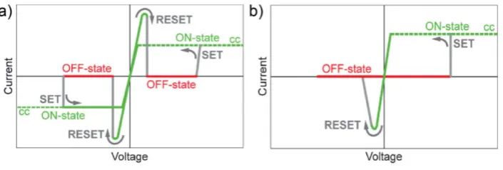
There are two types of switching: unipolar switching and bipolar switching. In unipolar switching devices, resistive switching occurs at different amplitudes of the same polarity. In bipolar switching devices, the polarity and amplitude of the signal are both important factors for switching. The current-voltage curves corresponding to unipolar and bipolar switching are shown in figure 2.2.
Figure 2.2: a) Unipolar switching. b) Bipolar switching. Figure taken from[9].
2.1.1
Filament and interface type switching
There are two mechanisms for (redox-based) resistive switching: filament type switching and interface type switching. These mechanisms model the origin of the changing resistive, and are still an active area of research.[10]
[image:10.595.104.457.472.591.2]Chapter 2. Theoretical aspects 2.1. Resistive switching
a path of oxygen vacancies – a conductive filament. The device is now in the LRS. To switch the device from the LRS to the HRS, the conductive filament is partially broken: oxygen atoms recombine with oxygen vacancies. To switch from LRS and HRS the partially broken conductive filament is restored by again pulling the oxygen atoms from the lattice of the MO to the TE. The forming and switching processes are illustrated in figure 2.3.
Initial state 1. Forming
2. HRS 3. LRS
Rupture TE
MO
BE
Figure 2.3: A schematic representation of the forming and switching processes of filament type switching. Image adapted from[11].
In interface type switching, the switching takes place at the interface. The metal electrodes influence the switching behaviour by participating in a redox reaction or in trapping oxygen vacancies.[8]When a filament cannot form, the contact resistances of the interfaces determine the resistance. To obtain resistive switch-ing, one interface should behave Ohmic and the other as a Schottky barrier. The barrier height of the Schottky barrier can be adjusted by applying a voltage. It has been reported that devices with PCMO as the metal-oxide layer only show resistive switching when combined with a low work function electrode.[12]
2.2. PCMO and the role of oxygen vacancies Chapter 2. Theoretical aspects
2.2
PCMO and the role of oxygen vacancies
PCMO (Pr1-xCaxMnO32) is a material that shows resistive switching behaviour of
interface type when sandwiched between two electrodes.[13][14]
In devices with a titanium TE a thin metal-oxide layer (TiO2) is formed
be-tween the PCMO and the TE. To date, PCMO devices have shown only bipolar switching, suggesting that this metal-oxide layer has a critical role in the resistive switching of PCMO-based devices. The resistance of the oxide layer in the LRS is small, but in the HRS the resistance of the oxide layer is large and dominates the device.
A possible explanation is as follows: oxygen vacancies transform the TiO2 layer from an insulator into a semiconductor. When a positive voltage is applied to the TE, the oxygen vacancies (positively charged) are driven out of the TiO2 to the
PCMO layer, changing the TiO2 layer from a semiconductor to an insulator. As a result the device switches from the LRS to the HRS. When a negative voltage is applied, the oxygen vacancies are attracted to the TiO2 layer and the device
switches from the HRS to the LRS.[13]This is illustrated in figure 2.4.
This mechanism also explains the direction of switching seen in figure 2.1. The device starts with the oxygen vacancies in the PCMO layer (LRS, line with highest current). After applying a potential the oxygen vacancies are moved to the TiO2
layer (HRS, line with lowest current). By applying a negative voltage, the reverse occurs, and the device switches from the HRS to the LRS (in the negative voltage region: line with lowest absolute current to line with highest absolute current).
= oxygen vacancy Metal oxide
Electrode
LRS HRS
+ -+
-Figure 2.4: A schematic representation of inter-face type switching. Top row: the two different resistance states. Bottom row: the switching processes.
2In this research Pr
Chapter 2. Theoretical aspects 2.2. PCMO and the role of oxygen vacancies
Chapter 3
Experimental aspects
3.1
Fabrication techniques
Before any measurements could take place, the devices had to be fabricated. Mainly sputtering, pulsed laser deposition and lithography were used for the fabrication of the devices. These techniques will be discussed in this section, as well as the exact process of fabricating a device.
3.1.1
Pulsed Laser Deposition
Pulsed laser deposition (PLD) is a technique used to deposit thin films. As its name suggests, it makes use of laser pulses. These pulses are sent to the target that is desired to be deposited, where the energy of the pulses will be absorbed. The absorbed energy releases the atoms on the surface of the target. The atoms will evaporate and ionize due to the high energies, and a plasma will form. The plume of this plasma, consisting of several particles such as energetic neutral atoms, ions, electrons and atom clusters, is highly directional. The content of the plume can therefore be propelled towards the substrate, where it will condensate and form a film. The substrate is heated to create more crystalline layers. At higher temperatures atoms can move more easily to a ‘hole’ in the substrate, therefore flatter layers are obtained when the substrate is heated.
The PLD process is operated in ultra high vacuum to reduce contaminations of the growing film. However some gases such as O2 and N2 are often released
into the deposition chamber to promote surface reactions or maintaining film stoichiometry.[16]
Figure 3.1 shows a schematic view of an example of a PLD system.
3.1.2
Radio frequency sputtering
Chapter 3. Experimental aspects 3.1. Fabrication techniques
Figure 3.1: Schematic view of a PLD system. Figure taken from[17]. An UV excimer beam shines (pulsed) on the target material to create a plasma plume. The CO2 is used to heat the
substrate. The DC stepper motor moves the target continuously to make sure that the UV excimer beam shines on all parts of the target to prevent the forming of holes.
Figure 3.2: Schematic view of a RF sputtering system. Figure taken from[18].
[image:15.595.204.415.425.601.2]3.1. Fabrication techniques Chapter 3. Experimental aspects
ions will be attracted more to the target and mainly atoms of the target will be sputtered. Those sputtered atoms will drop down and form a thin film on the substrate.
In this research a variation of RF sputtering called RF magnetron sputtering was used. In RF magnetron sputtering, magnets are added to the deposition chamber. Several magnet configurations are possible, but they all rely of the same principle. The magnetic field traps electrons and/or ions close to the sub-strate. This increases the probability of collisions between electrons, ions and atoms. In turn, this results in a denser plasma near the target. A denser plasma causes higher sputtering rates and thus higher deposition rates. Consequently, RF magnetron sputtering is faster than ordinary RF sputtering.[19]
[image:16.595.180.388.270.535.2](e) (d) (c) (b) (a)
Figure 3.3: Schematic overview of the lift-off process. (a) UV light passes through a reticle. (b) Some parts of the photoresist are exposed to the light (orange colour), other parts are not (red colour). (c) The non-exposed areas are removed. (d) A metal is deposited onto the sample. (e) Using lift-off, the exposed pho-toresist is removed along with unwanted metal depositions.
3.1.3
Lift-off lithography
Chapter 3. Experimental aspects 3.2. Preparation of the devices
several lithography techniques, only lift-off lithography will be discussed here. Lift-off lithography is mainly based on the properties of the photoresist. This is a substance that can be dissolved in certain solutions after1it is lighted by UV light.
Figure 3.3 shows the process of lift-off lithography. First, the sample is spin-coated with photoresist. UV light is then beamed at the sample through a reticle (mask) that contains the desired pattern. In figure 3.3 a negative photoresist is used. After placing the sample in development solvent, only the enlightened parts of the photoresist are left on the sample. Next, the desired layer(s) of materials are deposited on the sample by (for example) sputtering or PLD. Lastly, the sample is placed in ethanol and acetone to let the photoresist dissolve. The materials deposited directly on top of the photoresist will also be removed from the sample due to the dissolving photoresist underneath. The sample now has the same structure as the reticle.2
3.2
Preparation of the devices
To produce the RRAM devices used for this research, all of the fabrication tech-niques described in section 3.1 were used. The properties of all devices are shown in appendix A.
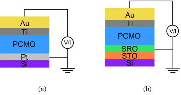
Devices 1-3 are similar in every aspect except the oxygen pressure during PCMO growth. The composition of devices 1-3 is shown in figure 3.4. The choice for this composition was based on previous research by others, which shows that a device with this composition is able to resistively switch between states.[8] Buffer layers are used to match the lattice parameters of mismatching layers.
The substrate of the device is a niobium (Nb) doped strontium titanate (SrTiO3,
commonly abbreviated as STO) layer. On this substrate, a 60nm thick layer of SrRuO3 was grown using PLD. Next, a 100nm thick PCMO layer was grown using
PLD. The oxygen pressure during the growth of the PCMO layer was different for devices 1-3. Device 1 was grown at an oxygen pressure of 0.2mBar, device 2 was grown at an oxygen pressure of 0.2mBar for 20nm then at 10-3mBar for 80nm, device 3 was grown at an oxygen pressure of 5×10⁻⁵mBar.
Next, photoresist was spincoated on the devices and using the method de-scribed earlier, the pattern of the electrodes was applied to the device. Three differently sized electrodes were applied: 50µm×50µm, 100µm×100µm and 200µm×200µm. Of each size, multiple electrodes were applied to the same device. The electrodes consist of 100nm gold (Au) on top of 16nm(top elec-trode)/18nm(bottom electode) titanium (Ti). Sputtering was used for the appli-cation of the electrodes. Lift-off lithography was used to remove unwanted Au and Ti.
1Or before, this depends on whether it is a ‘positive’ or ‘negative’ resist.
2This is true only when a negative photoresist is used. When a positive photoresist is used,
3.2. Preparation of the devices Chapter 3. Experimental aspects
Au Ti Au
Ti
PCMO
SRO
Nb-STO
[image:18.595.214.354.86.247.2]V/I
Figure 3.4: Schematic view of the layers of devices 1 - 3. Thicknesses are not to scale. Also shown is the application of the potential.
Finally, the device was glued to a metal plate using conducting glue. This makes attaching probes to the device easier. The device is now ready for measurement.
For devices 4 and 5 a similar process was used, although the composition of the devices is different. The structure of device 4 is: Au/Ti/PCMO/Pt/Ti/SiO2/Si,
PCMO was grown at an oxygen pressure of 10-3mBar. The structure of device 5 is: Au/Ti/PCMO/SRO/STO/Si, PCMO was grown at an oxygen pressure of 5×10⁻⁵mBar. The composition of devices 4 and 5 is shown in figure 3.5.
Devices 4 and 5 were produced on silicon to show that RRAM is compatible with current CMOS technology, which is produced (almost exclusively) on silicon wafers. CMOS technology is used in microprocessors, microcontrollers, logic circuits and other circuits.
V/I Au
Ti
PCMO
Pt
Si
(a)
V/I
Si Au
Ti
PCMO
SRO
STO
(b)
[image:18.595.131.421.555.707.2]Chapter 3. Experimental aspects 3.3. Characterization of the devices
Figure 3.6a shows a photograph of the device glued to the metal plate. Figure 3.6b shows a microscopic image of the device. The differently sized electrodes can clearly be seen.
(a) (b)
Figure 3.6: Images of the device. (a) Image showing the device glued to the metal plate. (b) Microscopic image of the device.
3.3
Characterization of the devices
To determine the performance of the devices, they have to be characterized. The devices are characterized in two ways: electrical characterization and structural characterization. Electrical characterization is concerned with the performance of the resistive switching behaviour, it is focused on the output of the device. The structural characterization is concerned with the structure of the device, this includes the crystallinity and morphology of the device.
To characterise the devices, several techniques are used, such as atomic force microscopy and X-ray diffraction. The techniques used for the characterization of the devices are described in this section.
3.3.1
Atomic Force Microscopy
Atomic force microscopy (AFM) is a technique that is widely used in various fields to image surfaces. The resolution of this technique can reach values smaller than 1nm (in the z-direction). AFM uses a tip attached to a cantilever. When the tip approaches the surface of the sample it gets attracted or repulsed by the surface. The attraction or repulsion is caused by the inter-atomic potential between the tip and surface, which only occurs for short distances between the tip and surface.
3.3. Characterization of the devices Chapter 3. Experimental aspects
detector. Since the cantilever can be considered a spring, the force on the tip can be determined by Hooke’s law:
F=−k x (3.1)
[image:20.595.137.436.201.344.2]A schematic view of an AFM is shown in figure 3.7. A feedback loop regulates the height of the sample such that the interaction force between tip and sample remains constant.[20]
Figure 3.7: Schematic view of an AFM. Figure taken from[20].
There are several measurement modes used in AFM imaging. In this research, the ‘tapping’ mode was used for imaging. In tapping mode the cantilever oscillates near its resonance frequency and the oscillation amplitude is 20-200 nm. The tip makes contact with the surface of the sample for a very short period of time in each oscillation. During this period of time, the tip-sample interaction changes the amplitude, resonance frequency and phase angle of the oscillating lever. The amplitude of the cantilever is chosen such that the probe has enough energy to pass back and forth through contamination on top of the sample.[20]
3.3.2
X-Ray Diffraction
X-ray diffraction (XRD) is a technique that is widely used to identify the atomic structure of samples. The technique is based on diffraction. When two incidental waves interfere (are in phase), a diffraction pattern appears. The condition for such an interference is given by Bragg’s law:
nλ=2d sinθ (3.2) Whereθ is the angle of incidence,λthe wavelength of the incidental light, d is the distance between two planes (of atoms) andnis an integer. Bragg’s law is illustrated in figure 3.8.
XRD is based on this principle. Light with a very low wavelength (X-rays) is sent into the sample. The intensity of the diffracted beam is measured. An XRD setup is shown schematically in figure 3.9a.
Chapter 3. Experimental aspects 3.3. Characterization of the devices
Figure 3.8: Schematic view of Bragg’s law. Fig-ure taken from[21].
The beam is diffracted by the sample (the crystal in figure 3.9) and is detected by an X-ray detector. The angle between the incident X-ray beam and the detector is defined as 2θ. In figure 3.9b the rotational axes with respect to the sample holder are shown. The detector and source can be rotated around these axes, the anglesΩand 2θ can also be varied. Measuring the intensity of the varied angles provides information about the sample. In this report only 2θ−Ωand Ωscans are discussed.
Figure 3.9: Schematic view of a XRD setup. Figure taken from[22].
2θ−Ωscan
During a 2θ−Ωscan both the detector and source are rotated in theωdirection. In this mode symmetrical reflexes (Ω=θ) are used. To maintain this property the detector and source move at the same angular velocity, but in opposite direction.
This technique is often used to determine the unit cell of the sample. The composition and strain of the layers in the sample can also be determined using this technique.[23]
Ωscan
[image:21.595.152.482.404.517.2]3.3. Characterization of the devices Chapter 3. Experimental aspects
and source therefore remains constant, but the angle between the sample and detector/source is varied.
From the rocking curve (intensity as a function ofω) the full width half maximum (FWHM) is often determined and used as a measure for the grain size of a sample.
For powder this size can be calculated exactly, but for thin film layers this is not possible. The FWHM can however be used to compare the grains of two samples.3[22]
3.3.3
Keithley 4200-SCS
The Keithley 4200-SCS was used to measure current-voltage sweeps and the stability of the devices. The Keithley allows the user to input a custom volt-age array that will be applied to the sample. Simultaneously, the Keithley will measure the current. This means that every desired voltage signal can be cre-ated and applied to the sample and the current can be measured at the same time.
The voltage lists used in this report were generated in MATLAB. Two signal types were used, these are described below.
Current-voltage sweep
The current-voltage sweep is a measurement in which the voltage is varied as follows: 0→ VMAX →0→ –VMAX→ 0, with linear steps between the mentioned
voltages.
Current-voltage sweeps were frequently used to check whether the current-voltage curve of a device shows a hysteresis (and therefore shows resistive switching behaviour), before doing longer measurements.
Current-voltage sweeps were also used to determine the stability of the devices. A signal of 200 sweeps was applied to the devices and the current was measured by the Keithley. The decay of the device can be determined by calculating the HRS/LRS-ratio at a certain voltage (VREAD) for each sweep. These measurements
were performed on all devices for all electrode sizes.
Pulses
Another signal that was used consists of pulses. The device is first SET by a large positive voltage, then READ by a lower voltage (can be either positive or negative), then RESET by a large negative voltage and finally READ once more (by the same voltage as the previous read signal). Thus: VSET → VREAD
→VRESET→ VREAD. The values of VSET, VRESET and VREAD were varied with each
measurement series.
A signal like this was used for the determination of the switching type of the devices (interface type or filament type). A signal consisting of 20 pulses was
3In figure 3.9 and in this text other symbols are used for the angles than the XRD in the Mesa+
NanoLab (PANalytical X’Pert3Powder). The XRD usesωinstead ofΩ. However, the definition of
Chapter 3. Experimental aspects 3.3. Characterization of the devices
applied to all electrode sizes. The mean value of the HRS and LRS (as determined by the first and second VREAD of each pulse) was determined, and compared to
that of other electrode sizes.
The stability of the devices was also determined by applying pulse signals. A signal of 1000 pulses was applied to the devices, again to all electrode sizes. The values of the HRS and LRS were determined and divided to obtain the HRS/LRS-ratio. The progression of the HRS/LRS-ratio over time or pulse gives an indication of the stability of the device.
A similar measurement as the one described above was also performed. In this case, the signal is slightly different: VSET → VREAD → –VREAD → VRESET →
VREAD → –VREAD. The sum of all the voltages in this signal is zero. This could result in less charge accumulation at the interfaces in the device, as the oxygen vacancies in the PCMO are attracted to both sides at the same rate. This could result in a better stability of the device. Processing the results is done similarly to that of the signal described above.
Chapter 4
Results
4.1
Switching type of PCMO-based devices
To determine the switching type of the devices –discussed in section 2.1.1– the elec-trode area dependence of the resistance was determined. A pulsed SET–READ– RE-SET–READ signal1 was applied to the electrode, and the corresponding current
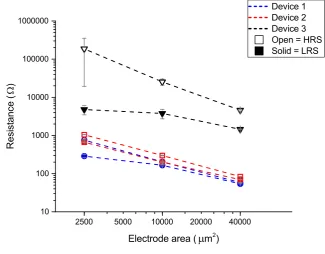
was measured. Using equation 2.1 the resistance values of the HRS and LRS were calculated. The resistance values are plotted as a function of electrode area in figure 4.1.
5000 20000
2500 10000 40000
10 100 1000 10000 100000 1000000
Device 1
Device 2
Device 3
Open = HRS
Solid = LRS
R
e
s
i
s
t
a
n
c
e
(
)
Electrode area ( m
2
[image:24.595.119.445.409.663.2])
Figure 4.1: Area dependence of the resistance of both the LRS and HRS of devices 1-3. Grey errorbars denote the standard deviation.
1V
SET=3V, VRESET=–3V, VREAD=–1V. The read voltage was chosen based on the HRS/
Chapter 4. Results 4.1. Switching type of PCMO-based devices
A linear dependence between the electrode area and resistance values can be seen in figure 4.1. This dependence is a characteristic of interface type switching.[9] It implies that the switching takes placed over the entire area of the electrode.
There are two points that deviate from the linear: the LRS 50µm electrode for both device 1 and device 3 is lower than predicted by the linear dependence. No clear reason was found for this deviation.
It can be concluded that the switching in devices 1-3 is of interface type. This confirms earlier results by others.[13][14]
The switching type of device 5, a device grown on a SRO/STO/Si-stack, was also determined using the same measurement method. The resulting area dependence of the resistance is shown in figure 4.2.
5000 20000
2500 10000 40000
10 100 1000 10000 100000 1000000
R
e
s
i
s
t
a
n
c
e
(
)
Electrode area ( m
2
)
Open = HRS
[image:25.595.152.472.309.561.2]Solid = LRS
Figure 4.2: Area dependence of the resistance of both the LRS and HRS of device 5.
The resistance is not dependent on the electrode area: it remains constant re-gardless of the electrode area. It looks as though this device shows filament type switching, but this seems unlikely. The device structure is nearly the same as the structure of devices 1-3, meaning that one would expect interface type switching to be the mechanism for this device as well.
It is possible that an error was made during the measurement, causing the resistance of another layer to be dominant over the TiO2 layer’s resistance,
4.2. Influence of oxygen pressure Chapter 4. Results
Another possibility is that this was caused by the lift-off process of device 5. The surface of device 5 shows irregularities not observed in any other device. It is suspected that either part of the PCMO layer was removed during the lift-off process or that there is some acetone left on the surface of the device. Either case may have influenced the results.
Both cases, however, do not give an explanation for the fact that there are two different resistance states, which indicated that resistive switching does take place and is measurable. More research on this device is needed to find the exact cause of this unlikely result.
4.2
Influence of oxygen pressure
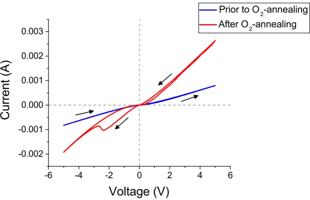
The importance of oxygen in PCMO for resistive switching became apparant when measuring device 2356.2 Prior to annealing3 the device with oxygen, the device showed almost no resistive switching: the hysteresis was very small. After annealing the device in air for one hour4, the device showed much better resistive switching characteristics. The size of the hysteresis increased, and the HRS/ LRS-ratio also increased. Prior to annealing the highest HRS/LRS-ratio achieved was approximately 1.7, after annealing the highest HRS/LRS-ratio achieved was approximately 15. A significant increase. The current-voltage sweeps are shown in figure 4.3.
2Device 2356 was not produced in-house, details of the device are unknown. The composition
is: Pt/Ti/PCMO/SRO/CeO2/YSZ/Si.
3Annealing is a process in which the device is heated to above its recrystallization temperature,
allowing it to undergo significant changes.
Chapter 4. Results 4.2. Influence of oxygen pressure
-6 -4 -2 0 2 4 6
-0.002 -0.001 0.000 0.001 0.002 0.003
C
u
r
r
e
n
t
(
A
)
Voltage (V)
Prior to O
2
-annealing
After O
2
[image:27.595.156.470.82.284.2]-annealing
Figure 4.3: Current-voltage sweeps of device 2356 prior to and after annealing with oxy-gen. The performance of the device increased greatly after O2-annealing. The arrows
indi-cate the switching polarity, which is the same for both measurements.
This result is consistent with earlier research by Kim, which states: “The resis-tance ratio of HRS and LRS was increased by oxygen annealing of the PCMO thin film.”.[24]There is, however, more recent research which found that hysteresis size does not keep increasing with increasing oxygen pressure, in other words: there is a maximum.[25]
More important than the size of the hysteresis is the obtained HRS/LRS-ratio. A large hysteresis could have a smaller HRS/LRS-ratio than a smaller hysteresis. In that case, the device with the bigger HRS/LRS-ratio (and smaller hysteresis) is better suited for resistive switching applications. Waser notes that HRS/ LRS-ratios>10 are required to compete with flash memory.[9]Other aspects, such as stability, are also very important.
While this is not a measurement that proves that resistive switching is dependent on oxygen pressure in one way or another –to do that more information about the device would be needed– it does show that there is reason to research the influence of oxygen pressure on the functioning of resistive switching devices.
4.2. Influence of oxygen pressure Chapter 4. Results
-4 -2 0 2 4
-0.06 -0.04 -0.02 0.00 0.02 C u r r e n t ( A ) Voltage (V) Device 1 Device 2 Device 3
-4 -2 0 2 4
[image:28.595.154.418.82.285.2]10 -10 10 -9 10 -8 10 -7 10 -6 10 -5 10 -4 10 -3 10 -2 10 -1 10 0 | C u r r e n t | ( A ) Voltage (V)
Figure 4.4: Current-voltage sweeps for devices with PCMO grown at various oxygen pressures. Device 1: 0.2mBar. Device 2: 0.2mBar for 20nm thickness then 10-3mBar for 80nm thick-ness. Device 3: 5×10⁻⁵mBar. The inset shows
the same sweeps plotted logarithmically. The arrows indicate the switching polarity.
Especially the positive side of the hysteresis seems dependent on the oxygen pressure during PCMO growth: its size increases significantly as the oxygen pressure increases. This is also true for the negative part of the hysteresis, but less so.
The HRS/LRS-ratio of device 3 is larger than those of device 1 and device 2. De-vice 1 has a maximum HRS/LRS-ratio of roughly 11, device 2 of roughly 16, while device 3 has values in the order of 200 or greater. Thus, if the HRS/LRS-ratio of the device is chosen as a performance indicator, devices with a lower oxygen pressures during PCMO growth perform better than those with a higher oxygen pressure during PCMO growth. Kim obtained the opposite result: the HRS/ LRS-ratio increases with oxygen pressure.[7]More importantly, all devices reach the minimum HRS/LRS-ratio (>10) required to compete with flash memory.
4.2.1
Inspection of devices
The structure of devices 1-3 was inspected using an AFM and XRD, both tech-niques are described in section 3. Both measurements were performed on the device prior to applying the electrodes.
Chapter 4. Results 4.2. Influence of oxygen pressure
1 µm 2 3 4
1 2 3 4 8.1 nm 2.0 3.0 4.0 5.0 6.0 7.0
(a) RMS=1.479nm
1 µm 2 3 4
1 2 3 4 15.0 nm 0.0 4.0 6.0 8.0 10.0 12.0
(b) RMS=2.199nm
1 µm 2 3 4
1 2 3 4 10 nm 0 2 3 4 5 6 7 8 9
[image:29.595.116.512.55.194.2](c) RMS=0.8964nm
Figure 4.5: AFM images of devices 1-3. (a) Device 1, oxygen pressure: 0.2mBar. (b) De-vice 2, oxygen pressure: 0.2mBar for 20nm thickness then 10-3mBar for 80nm thickness.
(c) Device 3, oxygen pressure: 5×10⁻⁵mBar.
Device 1 shows lines on the surface of the PCMO. The lines are 2-3nm high and approximately 300nm wide. Similar lines were imaged for Pr0.48Ca0.52MnO3
by Herpers.[1]Herpers also notes that similar lines to that of Pr0.48Ca0.52MnO3
appear for Pr0.7Ca0.3MnO3. Possible explanations are crystallographic domain
walls and crack formations. The lines for Pr0.48Ca0.52MnO3 are mostly aligned
parallel or perpendicular to the step edges of the underlying substrate.
It is also noted by Herpers that the lines for Pr0.48Ca0.52MnO3 seem to be
de-pendent on the thickness of the layer: for thin PCMO layers, the lines do not seem to appear. This results does not correspond with the results shown in figure 4.5. Lines appear only for device 1, while the PCMO layers of all devices are thicker (all equally thick: 100nm) than the PCMO layers used by Herpers (50nm) which all show lines.
While it is not clear what the exact cause of the lines is, it is possible that they might influence the resistive switching behaviour of the device. Not considering the lines, the PCMO layer of sample seems relatively flat compared to device 2 and 3 (the RMS of an area without lines is approximately 0.430nm).
Devices 2 and 3 show no lines, but do show some irregularities. Device 2 shows the largest irregularities of all devices. This device was grown at two oxygen pressures. This might be the cause of the relative roughness, as there might be a fundamental difference in the structure of the two layers. Device 3 is relatively flat.
4.2. Influence of oxygen pressure Chapter 4. Results
the grains are not clearly visible in figure 4.5, and hence this result cannot be confirmed.
Summarizing, device 3 is the flattest and grown at the lowest oxygen pressure. Device 2 is the roughest yet is not grown at the highest oxygen pressure. Device 1 is relatively flat and shows lines (which increase the roughness parameter).
Concluding, there is no clear dependence of the roughness of the PCMO surface on the oxygen pressure during growth. Neither is there a clear link between the roughness and performance of the devices. Devices with a small roughness parameter seem to perform better than devices with a large roughness parameter. Should that be true, it follows that the lines cause a significant reduction in the performance of the device.
Figure 4.6 shows the XRD results of devices 1-3. A 2θ-ω scan was made of each device. Each peak in figure 4.6 is identified by Miller indices, three numbers that correspond to a lattice plane.
Chapter 4. Results 4.2. Influence of oxygen pressure
40 45 50
[image:31.595.196.429.84.270.2]10 0 10 1 10 2 10 3 10 4 10 5 10 6 SRO (002) STO (002) PCMO (002) I n t e n s i t y ( C o u n t s / s ) 2 (Degrees) Device 1 Device 2 Device 3
Figure 4.6: 2θ-ω scans of devices 1-3. (a) De-vice 1, oxygen pressure: 0.2mBar. (b) DeDe-vice 2, oxygen pressure: 0.2mBar for 20nm thick-ness then 10-3mBar for 80nm thickness. (c) Device 3, oxygen pressure: 5×10⁻⁵mBar.
A rocking curve was made of each PCMO(002) peak. The full-width-half-maximum (FWHM) of such a scan gives an indication of the crystallinity of the PCMO. A smaller FWHM corresponds to a more crystalline material. The FWHM of the PCMO peaks are listed in table 4.1
Device FWHM (◦)
1 0.28067
2 (large peak) 0.36583 2 (small peak) 0.29339
3 0.35047
Table 4.1: FWHM of the rocking curves of the PCMO(002) peaks for devices 1-3.
[image:31.595.235.388.459.534.2]4.2. Influence of oxygen pressure Chapter 4. Results
4.2.2
Switching stability of devices 1-3
Pulse stability
A signal consisting of a thousand switching pulses5 was applied to the devices.
The HRS/LRS-ratio is plotted as a function of pulse number in figures 4.7a-4.9a. The corresponding progression of the resistance values of the HRS and LRS is shown in figures 4.7b-4.9b.
0 200 400 600 800 1000
0.8 1.0 1.2 1.4 1.6 1.8 2.0 2.2 2.4 2.6 2.8 3.0 50 m 100 m 200 m H R S / L R S Pulse number (a)
0 500 1000
65.8 70.5 75.2 79.9 340 510 680
0 500 1000
[image:32.595.116.481.189.420.2]1000 2000 3000 4000 Pulse number R e s i s t a n c e ( ) (b)
Figure 4.7: Stability measurements for device 1, which was grown in an oxygen pressure of 0.2mBar. (a) HRS/LRS-ratio as a function of pulse number. (b) Resistance values as a function of pulse numbers.
The stability of device 1 is insufficient for application: the HRS/LRS-ratio decays to one rapidly. The 50µm×50µm electrode decays more slowly than the other two electrode sizes. Furthermore, the difference between the HRS and LRS resistance values of the 100µm×100µm device is very small, indicating that either the switching properties of this electrode size are not sufficient, or that no (proper) switching occurs at all. Results for other devices with the same electrode size do show a bigger difference between the HRS and LRS resistance values (see figures 4.8b and 4.9b), indicating that the latter statement is true.
Device 2 also shows a strong decay. Compared to the results for device 1, the decay of the HRS/LRS-ratio for electrodes of sizes 100µm×100µm and 200µm×200µm is slower. However, for all electrode sizes, the HRS/LRS-ratio seems to converge to (nearly) one.
The results for device 3 are more promising, but also shows some odd behaviour. For the electrode of size 200µm×200µm the HRS/LRS-ratio rapidly rises during the first one hundred pulses, caused by a rising HRS resistance value. It is unclear what causes this rise. One possibility could be that oxygen vacancies are trapped
5V
Chapter 4. Results 4.2. Influence of oxygen pressure
0 200 400 600 800 1000
0.8 1.0 1.2 1.4 1.6 1.8 2.0 2.2 2.4 2.6 2.8 3.0 50 m 100 m 200 m H R S / L R S Pulse number (a)
0 500 1000
300 375 450 525 1000 1500 2000
0 500 1000
[image:33.595.134.508.81.375.2]3900 5200 6500 7800 Pulse number R e s i s t a n c e ( ) (b)
Figure 4.8: Stability measurements for device 2, which was grown in an oxygen pressure of 0.2mBar for 20nm thickness and then in an oxygen pressure of 10-3mBar for 80nm thick-ness. (a) HRS/LRS-ratio as a function of pulse number. (b) Resistance values as a function of pulse numbers.
in the TiO2 layer, lowering the resistance of the device. The device then switches
between the LRS and some state between the LRS and HRS, rather than between the LRS and HRS. As more pulses are applied, the oxygen vacancies are freed from the TiO2 layer, causing the HRS resistance value to increase.
The switching stability of device 3 is better than that of the other two devices. The HRS/LRS-ratio of the 100µm×100µm and 200µm×200µm device converge to a value of approximately 1.2, the HRS/LRS-ratio of the 50µm×50µm device converges to a value lower than one.
Waser notes that flash memory has a maximum number of write cycles of 103 to 107, depending on the type.[9] None of the devices discussed here reaches
the minimum number of write cycles: 103, the devices here are unfit to compete with flash memory.
In conclusion:
i. All devices show a rapid decay of the HRS/LRS-ratio. The devices do not reach the required amount of cycles to compete with flash memory. ii. There is no clear indication that one electrode size is better than the other,
based on stability of the HRS/LRS-ratio.
4.2. Influence of oxygen pressure Chapter 4. Results
0 200 400 600 800 1000
0 10 20 30 40 50 60 50 m 100 m 200 m H R S / L R S Pulse number (a)
0 500 1000
62000 124000 186000 10000 20000 30000
0 500 1000
[image:34.595.113.480.77.287.2]25000 50000 75000 Pulse number R e s i s t a n c e ( ) (b)
Figure 4.9: Stability measurements for device 3, which was grown in an oxygen pressure of 5×10⁻⁵mBar. (a) HRS/LRS-ratio as a function of pulse number. (b) Resistance values as a function of pulse numbers.
the difference between the results of Liao and Chen and the results presented in this report lies in the length of a single READ signal. Other researchers use READ signals in the 50ns range, while a READ signal duration of approximately 8ms was used here.6 Waser notes that the read operation should be shorter than the write operation and should preferably be shorter than 100ns.[9]. A long READ signal might cause unwanted oxygen vacancy movements, causing a decay of the stability of the devices.
Previous research shows that a reduction of the HRS/LRS-ratio is most often caused by a decrease of the HRS, which is also seen in figures 4.7a-4.9a. The final failure is then caused by the device being stuck in the LRS, unable to switch to the HRS. A possible explanation for this failure is that too many oxygen vacancies are accumulated during the switching at the electrode-MO interface. In some cases the LRS resistance value also tends to increase, which might be caused by the formation of an oxide layer between the electrode and the metal-oxide.[10] It seems that the initial increase of the HRS resistance value in figure 4.9b is the reverse of the process described here.
Effect of input signal on stability
In the previous section the total sum of the voltages of the applied signal is not zero. To measure the impact of this on the stability of the device, a signal was created were the total sum of the voltages is zero, as described in section 3.3.3. This was achieved by counteracting every READ signal by applying a signal of the same amplitude but opposite polarity, directly after applying the READ signal.
Chapter 4. Results 4.2. Influence of oxygen pressure
The measurements were performed on device 3, which showed the highest resistance values. A READ signal of VREAD =–1V was applied. Figure 4.10 shows
the HRS/LRS-ratios of the ‘total sum zero’ signal (from now on: TSZ signal) and the signal used in the previous section.
0 200 400 600
0 5 10 15 20 25
Total sum < 0
Total sum = 0
H R S / L R S Pulse number (a)
0 200 400 600
0 20 40 60 80 100 120 140 160 H R S / L R S Pulse number
Total sum < 0 Total sum = 0
(b)
0 200 400 600
0 5 10 15 20 25 30 35 40 45 50 55 60 H R S / L R S Pulse number
Total sum < 0 Total sum = 0
(c)
Figure 4.10: Comparison of stability mea-surements for device 3. The blue line indi-cates the measurements using the TSZ signal. HRS/LRS-ratio as a function of pulse number for the (a) 50µm×50µm (b) 100µm×100µm (c) 200µm×200µm electrode.
Two interesting results can be seen in figure 4.10. First, for the 200µm×200µm electrode, the TSZ signal has a HRS/LRS-ratio higher than one for the entire duration of measurements. The HRS/LRS-ratio eventually reaches a value of around five, but is still decreasing.
This result cannot be attributed to the new signal-type, as the results for the 50µm×50µm and 100µm×100µm show the HRS/LRS-ratio converging to one. No change in the converging behaviour compared to the original signal was observed for these electrode sizes.
The second interesting result is that the rapidly rising HRS/LRS-ratio, also ob-served in figure 4.9a, can be seen in figure 4.10b and 4.10c. Interestingly, in figure 4.10b it is the TSZ signal that shows a rising HRS/LRS-ratio, while in figure 4.10c it is the original signal that shows a rising HRS/LRS-ratio. The 50µm×50µm electrode, shown in figure 4.10a, shows no similar behaviour, but does show a massive peak at the second pulse (about an order larger than the y-axis range).
[image:35.595.131.522.175.427.2]4.2. Influence of oxygen pressure Chapter 4. Results
case, two-hundred current-voltage sweeps were applied to the device.7 From
these sweeps, the HRS/LRS-ratio was determined at a certain voltage (the READ voltage). Figure 4.11 shows these results, it also includes the results of figure 4.10.
0 50 100 150 200
0 100 200 300 400 500 600 700 800 H R S / L R S Pulse/sweep number
Total sum < 0 Total sum = 0 Sweeps
(a)
0 50 100 150 200
0 100 200 300 400 500 600 700 800 H R S / L R S Pulse/sweep number
Total sum < 0 Total sum = 0 Sweeps
(b)
0 50 100 150 200
0 20 40 60 H R S / L R S Pulse/sweep number
Total sum < 0 Total sum = 0
Sweeps
[image:36.595.100.490.151.432.2](c)
Figure 4.11: Comparison of stability measure-ments for device 3. The blue line indicates the measurements of the previous section, the red line indicates measurements where the total sum of the voltage is zero, the black line indi-cates values determined from repeated sweeps. HRS/LRS ratio as a function of pulse number for: (a) 50µm×50µm (b) 100µm×100µm (c) 200µm×200µm.
For the electrodes of sizes 50µm×50µm and 100µm×100µm the sweep tech-nique seems to have a better stability, that is: the HRS/LRS-ratio is larger than the other techniques (pulses) initially, then all converge to the same value. The HRS/LRS-ratio of the sweep technique is quite unstable and also very large.
For the 200µm×200µm electrode the sweep technique performs worse than the pulse techniques. The HRS/LRS-ratio is lower than the pulse techniques for most of the range. The TSZ signal performs best here: averaging at about a HRS/LRS-ratio of 10 for the measured range. It is important to note that the sweep technique does converge to a very stable HRS/LRS-ratio of about 3.3 for this measurement. However, the TSZ signal HRS/LRS-ratio is higher over the entire measured range, and seems to converge to a value higher than one.
In conclusion, there does seem to be some dependence on the input signal, but is unclear what the exact dependence is. The best performing signals are the TSZ signal and the sweep signal.
7Only 200 sweeps were applied due to the maximum length of the voltage list in the Keithley.
Chapter 4. Results 4.2. Influence of oxygen pressure
4.2.3
Retention
The retention was studied for device 3. The results of this experiment are shown in table 4.2, 4.3 and 4.4. The device was SET (RESET) by a pulse of VSET =
3V (VRESET=–3V) and read by VREAD =–1V. The device was then left alone for
approximately 1.5 hours and read again.
For the biggest electrodes (200µm×200µm), both the resistance values of the HRS and LRS are decreasing over time. The decrease of the HRS is higher than the decrease of the LRS. The change in the resistance of the 100µm×100µm elec-trodes is different, most of them increase (slightly). But one electrode decreases. For the smallest electrodes (50µm×50µm), the resistance again decreases over time, except for one electrode. However, that increase is very small (only 2%), hence the electrode can be said to be stable.
In general, the retention of device 3 not sufficient for application: the resis-tance of both the HRS and LRS changes significantly over time. This makes the device unfit for use as a RRAM device as the retention time of non-volatile memory should be longer than at least 10 years.[27]
Voltage Rinitial (Ω) Rafter 1.5 hours(Ω) Change
3V SET 3862 2107 –45%
5850 3214 –45%
-3V RESET 764 689 –9.8%
[image:37.595.173.451.350.426.2]1190 1052 –11%
Table 4.2: Retention of two 200µm×200µm electrodes of device 3.
Voltage Rinitial (Ω) Rafter 1.5 hours(Ω) Change
3V SET 22088 27130 +23%
25827 15151 –41%
-3V RESET 2953 3167 +7.2%
[image:37.595.171.454.486.562.2]2295 22018 +859%
Table 4.3: Retention of two 100µm×100µm electrodes of device 3.
Voltage Rinitial (Ω) Rafter 1.5 hours(Ω) Change
3V SET 52612 53711 +2.1%
93888 508 –99%
-3V RESET 7066 2093 –70%
6982 367 –94%
Table 4.4: Retention of two 50µm×50µm elec-trodes of device 3.
[image:37.595.172.453.620.696.2]4.3. Devices on silicon substrate Chapter 4. Results
the resistance remained constant for at least one hour.[8]Cheng measured the retention of a Ni/GeO/HfON/TaN device that is much better than that of device 3: after 104seconds the resistance of the device started to change slightly.[28]
4.3
Devices on silicon substrate
Two devices were grown on a silicon substrate. One was grown on a Pt/Ti/SiO2/ Si-stack (device 4), the other on a SRO/STO/Si-stack (device 5). Only device 5 shows functioning resistive switching, see figure 4.12.
-1.0 -0.5 0.0 0.5 1.0
-0.10 -0.05 0.00 0.05 0.10 C u r r e n t ( A ) Voltage (V) (a)
-6 -4 -2 0 2 4 6
[image:38.595.100.440.235.487.2]-0.050 -0.025 0.000 0.025 C u r r e n t ( A ) Voltage (V) (b)
Figure 4.12: Switching in devices on a silicon substrate. (a) Device 4: no switching. PCMO grown on Pt/Ti/SiO2/Si-stack. (b) Device 5: switching. PCMO grown on SRO/STO/ Si-stack. The arrows indicate the switching po-larity.
Kim also uses a device with PCMO grown on Pt/Ti/SiO2/Si-stack.[7]Kim’s device
shows better resistive switching: the resistance value are higher and the ratio between the HRS and LRS is greater. A probable cause of this is the oxygen pres-sure during PCMO growth. Kim uses a minimum oxygen prespres-sure of 100mTorr during PCMO growth, whereas the PCMO layer in device 4 was grown at an oxygen pressure of 0.75mTorr (10-3mBar). While this might be the cause of the difference between Kim’s results and the results for device 4, it does not explain why device 5 does show resistive switching. The PCMO in device 5 was grown at the same pressure as device 4, yet shows resistive switching. This indicates that the structure of the device may be related to the performance of the device.
The PCMO layer of both devices was imaged using an AFM. These images are shown in figure 4.13.
Chapter 4. Results 4.3. Devices on silicon substrate
0 µm 1 2 3 4 0 1 2 3 4 28.0 nm 0.0 5.0 10.0 15.0 20.0 25.0
(a) RMS=1.590 nm
0 µm 1 2 3 4 0 1 2 3 4 11 nm 0 2 3 4 5 6 7 8 9 10
[image:39.595.121.486.50.230.2](b) RMS=1.102 nm
Figure 4.13: AFM images of devices 4 and 5. (a) Device 4: PCMO grown on Pt/Ti/SiO2/ Si-stack. (b) Device 5: PCMO grown on SRO/STO/Si-stack.
It is not possible to say why one device shows resistive switching while the other does not based purely on the AFM images. It has to be noted that the flatter PCMO layer (that of device 5) performs better than the rougher PCMO layer (that of device 4). This conforms to the statement made in section 4.2.1: “Devices with a small roughness parameter seem to perform better than devices with a large roughness parameter.".
XRD measurements were also made of the devices, prior to applying the electrodes. Figure 4.14 show the 2θ-ωmeasurement results for devices 4 and 5.
30 40 50 60 70 80
10 0 10 1 10 2 10 3 10 4 10 5 I n t e n s i t y ( C o u n t s / s ) 2 (Degrees) Si (400) Pt (111) PCMO (110) (a)
30 40 50 60 70 80
[image:39.595.159.504.487.740.2]10 0 10 1 10 2 10 3 10 4 10 5 I n t e n s i t y ( C o u n t s / s ) 2 (Degrees) Si (400) STO (002) PCMO (002) PCMO (110) (b)
Figure 4.14: 2θ − ω scans of devices 4 and 5. (a) Device 4: PCMO grown on Pt/Ti/SiO2/Si-stack. (b) Device 5: PCMO grown on SRO/STO/Si-stack.
4.3. Devices on silicon substrate Chapter 4. Results
difference between devices 4 and 5 is that device 4 only contains PCMO(110), while device 5 contains both (110) and –primarily– (002) oriented PCMO. De-vices 1-3 contain only (002) oriented PCMO, and show RS behaviour. Device 5 also shows RS behaviour, device 4 does not. This suggests that the (110) orien-tation of the PCMO in device 4 might be the cause of the insufficient performance.
Kim uses a device that has a composition similar to that of device 4. This device does show resistive switching. In Kim’s case, the PCMO is (112) oriented. This suggests either that the orientation of the PCMO in the device is crucial to device performance, or that other aspects (such as the oxygen pressure during growth) are crucial to device performance.
Li states that the (110) and (001) orientations of PCMO have the best resis-tive switching properties due to their high density of manganese atoms.[29]
The FWHM of the rocking curves of the PCMO peaks in figure 4.14 is shown in table 4.5. Compared to the values of devices 1-3 (table 4.1), the values for devices 4 and 5 are quite large, this is especially true for the FWHM of the PCMO(110) peak in device 4. This means that device 4 is less crystalline than the other devices.
Device FWHM (◦) 4 PCMO(110) 3.8802 5 PCMO(002) 1.0685
Table 4.5: Full-width-half-maximum of the rocking curves of the PCMO peaks for devices 4 and 5.
Due to the low crystallinity, a leakage current can occur. While switching might still occur, the effect cannot be observed due to the leakage current. This leads to current-voltage sweeps such as in figure 4.12a.
This means an argument can be made that the performance of the devices is not dependent on the orientation of the PCMO layer, but dependent on the crys-tallinity of the PCMO layer. However, this argument fails based on the results for devices 1-3, where large differences were observed in the performance of the devices, yet the crystallinity of the devices was approximately the same for all devices.
4.3.1
Stability measurements of device 5
To compare the functioning device (device 5) with devices 1-3, a stability mea-surement was performed, the results of which are shown in figure 4.15.
The device performs quite well: the HRS/LRS-ratio does not converge to one for both measurement methods. Instead, the value converges to approximately 3 in case of the pulse measurements and 3.5 in case of the sweep measurements.8
8Note that the sweep measurement only switches 200 times, while the pulse measurement
Chapter 4. Results 4.3. Devices on silicon substrate
0 200 400 600 800 1000
0 10 20 30 40 50 H R S / L R S Pulse number
0 500 1000
0 5000 10000 15000 20000 25000 R e s is t a n c e ( ) Pulse number (a)
0 50 100 150 200
[image:41.595.154.500.84.262.2]0 10 20 30 40 50 60 H R S / L R S Sweep number (b)
Figure 4.15: Stability measurements for de-vice 5 using the 50µm×50µm electrode. (a) Pulse stability, inset: progression of HRS and LRS resistance values. The same input signal type as in section 4.2.2 was used. (b) Sweep stability.
There is some variation in the value of the HRS/LRS-ratio, mainly caused by a fluctuation of the HRS resistance values. This should not necessarily be a problem for application of the device as RRAM.
Chapter 5
Conclusion
Based on the results, discussed in section 4, the following can be concluded about the devices researched in this report:
i. PCMO grown on a SRO/Nb-STO-stack shows interface type switching. See figure 4.1.
Concerning the influence of the oxygen pressure during PCMO growth:
ii. The level of oxygen in the PCMO layer is of influence on the resistive switching characteristics of the device. See figure 4.3 and figure 4.4. iii. Devices with a small roughness parameter seem to perform better than
devices with a large roughness parameter. More measurements are needed to confirm this.
iv. The crystallinity of PCMO is dependent of the oxygen pressure during growth. The crystallinity becomes better as the oxygen pressure is increased. See table 4.1.
v. The performance of RRAM devices is inversely related to the crystallinity of the PCMO.
vi. Stability is not influenced by the oxygen pressure during PCMO growth: devices 1-3 all converge to a HRS/LRS-ratio of one.
vii. Stability of the device increases when using the sweep or TSZ signal com-pared to a normal pulse signal.
Concerning the potential of devices 1-3 as commercial RRAM:
viii. The retention of information over time of device 3 is insufficient.
Concerning devices grown on silicon substrates:
ix. Devices grown on a SRO/STO/Si-stack perform better than devices grown on a Pt/Ti/SiO2/Si-stack. It is possible that this is caused by the orientation of the PCMO: (002) oriented PCMO seems to perform better than (110) oriented PCMO. Another possibility is that this is caused by the crystallinity of the PCMO. More measurements are required to verify which (if either) is true.
Chapter 5. Conclusion
report. The HRS/LRS-ratio converges to a value of approximately 3.0–3.5.
In short, the main conclusions are:
• PCMO-based RRAM devices are dependent on the oxygen pressure during PCMO growth. Performance seems to increase as oxygen pressure decreases. The HRS/LRS-ratio of the device reaches high enough values to compete with flash memory. The retention and stability of the devices are not able to compete with flash memory. More research is needed to create commercially viable devices.
Chapter 6
Discussion
6.1
Obstacles
Several obstacles were encountered during this research which might have influ-enced the results. In this section these obstacles will be described.
During the lift-off process of device 5 something went wrong, resulting in oddly shaped electrodes. While these electrodes were not used for measurements, this error might still have influenced the results. The error was observed due to differ-ent surface colours. It is suspected that the PCMO layer was partly removed on some areas of the device, taking (parts of) electrodes with it. Another possibility is that there is still some acetone left on the surface of the device.
The resolution of the AFM was too low to image individual grains of the PCMO layers. As grains are a good measure of the crystallinity of the PCMO layer, it would have payed off to measure at a higher resolution.
As already shortly noted in chapter 4, the Keithley 4200-SCS placed some restric-tions on possible measurements. The maximum bin size of a signal that can be applied by the Keithley is 4096 bins. This means long measurements cannot be performed, unless the signal is manually executed several times. This results in rest periods between measurements in which the PCMO layer has time to stabilize, influencing the results.
A second problem with the Keithley is that there is no fixed time period per bin. This is especially a problem when a signal consists of pulses, as pulse dura-tion varies when using the Keithley. This could result in asymmetry in oxygen vacancy transport, and hence could result in an accumulation of oxygen vacan-cies at one electrode. Such an accumulation might cause a decrease in device performance.
Chapter 6. Discussion 6.2. Proposed further research
Connecting a function generator to the Keithley could solve these problems. A function generator can generate signals with a fixed frequency. Unfortunately, due to time restrictions, this has not been tested.
6.2
Proposed further research
In this section, several propositions for further research are discussed.
To determine the influence of the roughness parameter of the PCMO layer more devices should be grown with different roughness parameters should be grown and their performance should be measured. The roughness parameter can be varied by growing the PCMO layer at various oxygen pressures.
To fully determine the influence of the orientation of the PCMO layer on de-vice performance, more measurements should be performed. More dede-vices with varying orientations should be grown. This can be achieved by using differently oriented substrates.
As mentioned in the previous section, measurements with shorter SET, RESET and READ pulses should be done to see whether the device performs well with current standards in electronics for pulse duration.
Acknowledgements
References
[1] A. Herpers. “Electrical characterization of manganite and titanate het-erostructures”. PhD thesis. Rheinisch-Westfälischen Technischen Hochschule Aachen, 2014.
[2] T. Mikolajick et al. “FeRAM technology for high density applications”. In:
Microelectronics Reliability 41.7 (2001), pp. 947 –950. DOI:
10.1016/
S0026-2714(01)00049-X
.[3] Jian-Gang Zhu. “Magnetoresistive Random Access Memory: The Path to Competitiveness and Scalability”. In:Proceedings of the IEEE96.11 (2008), pp. 1786–1798.DOI:
10.1109/JPROC.2008.2004313
.[4] Panasonic.Panasonic Starts World’s First Mass Production of ReRAM Mounted Microcomputers. July 2013. URL:
http : / / news . panasonic . com /
press / news / official . data / data . dir / 2013 / 07 / en130730
-2/en130730-2.html#1
.[5] R. Fackenthal et al. “19.7 A 16Gb ReRAM with 200MB/s write and 1GB/s read in 27nm technology”. In: Solid-State Circuits Conference Digest of Technical Papers (ISSCC), 2014 IEEE International. 2014, pp. 338–339.DOI:
10.1109/ISSCC.2014.6757460
.[6] Y. Kim et al. “Influence of Deposition Temperature and Substrate Orienta-tion on the Microstructure of Pr0.7Ca0.3MnO3 Films Grown on Platinum Substrates by Using Pulsed Laser Deposition”. In:Journal of the Korean Physical Society54 (2009), pp. 209–214.
[7] D. Kim et al. “Growth and characterization of Pr0.7Ca0.3MnO3 thin films for resistance random acces memory”. In:Journal of the Korean Physical Society49 (2006), S557–S561.DOI:
10.3938/jkps.49.557
.[8] Z. Liao. “The effects of spatial confinement and oxygen stoichiometry on complex metal oxides”. PhD thesis. Louisiana State University, 2012. [9] R. Waser et al. “Redox-Based Resistive Switching Memories –Nanoionic
Mechanisms, Prospects, and Challenges”. In:Advanced Materials21.25-26 (2009), pp. 2632–2663.DOI:
10.1002/adma.200900375
.[10] H. Wong et al. “Metal-Oxide RRAM”. In: Proceedings of the IEEE100.6 (2012), pp. 1951–1970.DOI:
10.1109/JPROC.2012.2190369
.[11] A. Sawa. “Resistive switching in transition metal oxides”. In: Materials Today11.6 (2008), pp. 28–36.DOI:
References References
[12] F. Pan et al. “Nonvolatile resistive switching memories-characteristics, mechanisms and challenger”. In: Progress in Natural Science: Materials International 20.0 (2010), pp. 1–15. DOI:
10.1016/S1002-0071(12)
60001-X
.[13] Z. Liao et al. “Categorization of resistive switching of metal-Pr0.7Ca0.3MnO3-devices”. In: Applied Physics Letters 94.25 (2009). DOI:
10 . 1063 / 1 .
3159471
.[14] A. Sawa et al. “Hysteretic current-voltage characteristics and resistance switching at a rectifying Ti/Pr0.7Ca0.3MnO3 interface”. In:Applied Physics Letters85.18 (2004), pp. 4073–4075.DOI:
10.1063/1.1812580
.[15] A. Herpers et al. “Spectroscopic Proof of the Correlation between Redox-State and Charge-Carrier Transport at the Interface of Resistively Switching Ti/PCMO Devices”. In:Advanced Materials26.17 (2014), pp. 2730–2735.
DOI:
10.1002/adma.201304054
.[16] M. Ohring. “Chapter 3 - Thin-film evaporation processes”. In:Materials Science of Thin Films (Second Edition). Second Edition. San Diego: Academic Press, 2002, pp. 95 –144.ISBN: 978-0-12-524975-1.DOI:
10.1016/B978-012524975-1/50006-9
.[17] R. Eason et al. “Multi-beam pulsed laser deposition for advanced thin-film optical waveguides”. In: Journal of Physics D: Applied Physics3 (2014), p. 034007. DOI:
10.1088/0022-3727/47/3/034007
.[18] M. Ohring. “Chapter 4 - Discharges, plasmas, and ion-surface interactions”. In:Materials Science of Thin Films (Second Edition). Second Edition. San Diego: Academic Press, 2002, pp. 145 –202. ISBN: 978-0-12-524975-1.
DOI:
10.1016/B978-012524975-1/50007-0
.[19] P. Kelly and R. Arnell. “Magnetron sputtering: a review of recent devel-opments and applications”. In: Vacuum56.3 (2000), pp. 159–172. DOI:
10.1016/S0042-207X(99)00189-X
.[20] R. Jagtap and A. Ambre. “Overview literature on atomic force microscopy (AFM): Basic and its important applications for polymer characterization”. In:Indian Journal of Engineering and Materials Science13 (2006), pp. 368– 384.
[21] D. Leadley. X-Ray Diffraction. 2009. URL:
http://www2.warwick.ac.
uk/fac/sci/physics/current/postgraduate/regs/mpags/ex5/
techniques/structural/xrd/
.[22] Fortgeschrittenpraktikum High Resolution X-Ray Diffraction. Technische Unversität München. 2009.
[23] M. Sardela. “X-ray analysis methods”. In:Advanced Materials Characteriza-tion Workshop, The Frederick Seitz Materials Research Laboratory–University of Illinois at Urbana-Champaign. 2008.
References References
[25] K. Choi et al. “Microstructure and resistive switching behaviour of amor-phous Pr0.7Ca 0.3MnO3 films grown under various oxygen pressures”. In: ECS Solid State Letters 2.7 (2013), N21–N25. DOI:
10 . 1149 / 2 .
003307ssl
.[26] Y. Chen et al. “PCMO Device With High Switching Stability”. In:Electron Device Letters, IEEE31.8 (2010), pp. 866–868. DOI:
10.1109/LED.2010.
2050457
.[27] D. Panda and T. Tseng. “Perovskite Oxides as Resistive Switching Memories: A Review”. In: Ferroelectrics 471.1 (2014), pp. 23–64. DOI:
10.1080/
00150193.2014.922389
.[28] C. Cheng et al. “High performance ultra-low energy RRAM with good reten-tion and endurance”. In:Electron Devices Meeting (IEDM), 2010 IEEE Inter-national. 2010, pp. 19.4.1–19.4.4. DOI:
![Figure 3.1: Schematic view of a PLD system.Figure taken from [17]. An UV excimer beamshines (pulsed) on the target material to createa plasma plume](https://thumb-us.123doks.com/thumbv2/123dok_us/9812207.482435/15.595.204.415.425.601/figure-schematic-figure-excimer-beamshines-pulsed-material-createa.webp)


![Figure 3.7: Schematic view of an AFM. Figuretaken from [20].](https://thumb-us.123doks.com/thumbv2/123dok_us/9812207.482435/20.595.137.436.201.344/figure-schematic-view-afm-figuretaken.webp)
![Figure 3.8: Schematic view of Bragg’s law. Fig-ure taken from [21].](https://thumb-us.123doks.com/thumbv2/123dok_us/9812207.482435/21.595.152.482.404.517/figure-schematic-view-bragg-law-fig-ure-taken.webp)