Ultrafast Band Structure Control of a
Two-Dimensional Heterostructure
Søren Ulstrup,
†Antonija Grubiˇsi´
c ˇ
Cabo,
‡Jill A. Miwa,
‡Jonathon M. Riley,
¶Signe S. Grønborg,
‡Jens C. Johannsen,
§Cephise Cacho,
kOliver Alexander,
kRichard T. Chapman,
kEmma Springate,
kMarco Bianchi,
‡Maciej Dendzik,
‡Jeppe V. Lauritsen,
‡Phil D. C. King,
¶and Philip Hofmann
∗,‡†Advanced Light Source, E. O. Lawrence Berkeley National Laboratory, Berkeley, California 94720, USA
‡Department of Physics and Astronomy, Interdisciplinary Nanoscience Center, Aarhus University, 8000 Aarhus C, Denmark
¶SUPA, School of Physics and Astronomy, University of St. Andrews, St. Andrews, United Kingdom
§Institute of Condensed Matter Physics, ´Ecole Polytechnique F´ed´erale de Lausanne (EPFL), Switzerland
kCentral Laser Facility, STFC Rutherford Appleton Laboratory, Harwell, United Kingdom
Abstract
The electronic structure of two-dimensional (2D) semiconductors can be
signifi-cantly altered by screening effects, either from free charge carriers in the material
itself, or by environmental screening from the surrounding medium. The physical
properties of 2D semiconductors placed in a heterostructure with other 2D materials
are therefore governed by a complex interplay of both intra- and inter-layer
interac-tions. Here, using time- and angle-resolved photoemission, we are able to isolate both
the layer-resolved band structure and, more importantly, the transient band structure
evolution of a model 2D heterostructure formed of a single layer of MoS2 on graphene.
Our results reveal a pronounced renormalization of the quasiparticle gap of the MoS2
layer. Following optical excitation, the band gap is reduced by up to ∼400 meV on
femtosecond timescales due to a persistence of strong electronic interactions despite
the environmental screening by the n-doped graphene. This points to a large degree of tuneability of both the electronic structure and electron dynamics for 2D
semicon-ductors embedded in a van der Waals-bonded heterostructure.
KEYWORDS: Ultrafast time- and angle-resolved photoemission, band gap
Van der Waals-bonded heterostructures of two-dimensional (2D) atomic sheets hold great
promise for the bottom-up design of materials with new properties.1–3 Realising
heterostruc-tures with desired functionality, however, remains a formidable challenge. Environmental
screening from neighbouring layers can severely modify the band structures of the individual
2D materials, even though no real chemical bonds are formed between them.4In 2D
semicon-ductors the quasiparticle band gap and the exciton binding energy have been observed to be
strongly influenced both by the choice of substrate material and by excited electrons within
the 2D material.5–8 When placing a single layer transition metal dichalcogenide (SL-TMDC)
on a metallic substrate such as Au(111), a strong band gap renormalization is observed but
the reduced band gap is almost unaffected by an additional excited carrier density.9,10 When
the SL-TMDC is placed on a weakly screening insulator such as SiO2, the static band gap is
close to that expected for the free-standing case11–13 but optically excited carriers can give
rise to a giant band gap reduction.6 Such carrier-induced renormalization effects are
some-what similar to some-what is observed in bulk semiconductors14 and quantum wells,15,16 where
they can be used to generate materials with non-linear optical properties. A key advantage
of using a truly 2D semiconductor, however, is that its environment can be freely chosen,
which should greatly enhance the tuneability of the system. We demonstrate this capability
for a heterostructure of SL MoS2and graphene (MoS2/G). Screening of the semiconductor by
the adjacent graphene is expected to induce a moderate reduction of the quasiparticle band
gap,4,17yet we find that the MoS
2 layer retains a strong optical tuneability. Using time- and
angle-resolved photoemission (TR-ARPES), we not only directly visualise how this causes
the band structure to change on femtosecond time scales following optical excitation of free
charge carriers, but are also able to separate the underlying electronic structure and carrier
dynamics from the SL MoS2 and the graphene.
In TR-ARPES, electrons are excited into unoccupied states using low-energy photons
and then photoemitted with a time-delayed higher energy laser pulse. This type of
equilibrium and excited states, and on the time dependent population change after the
ini-tial excitation. For the material system and moderate excitation studied here, one does not
typically expect the pump pulse to create changes in the band structure as such, but merely
in the population of the states. This is indeed what we find for the graphene layer in our
MoS2/G heterostructure: Electrons are pumped into the conduction band (CB) and follow a
decay dynamics that closely resembles earlier findings for epitaxial graphene.18On the other
hand, the adjacent MoS2 bands are rigidly shifted in the presence of the excited carriers. We
determine how these band shifts lead to a significant reduction of the quasiparticle band gap
as a function of the excited carrier density, consistent with a recent theoretical calculation.5
Results and Discussion
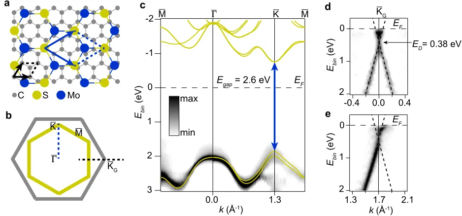
The MoS2/G heterostructure was grown on a silicon carbide substrate by van der Waals
epitaxy (see Materials and Methods section). Due to the weak interaction between the
individual 2D layers the MoS2 grows with many rotational domains. However, our synthesis
method yields a preference for MoS2domains that can be rotated by 30◦and 90◦with respect
to the underlying graphene (see sketch of the 30◦ case in Figure 1a). As described in detail
in Ref. 19 we can determine this rotational preference directly from ARPES scans of the
overlapping BZs of the two materials since both the Dirac cone of graphene and the valence
band maximum (VBM) of SL MoS2 are found at the ¯K point of their respective BZs (see
Figure 1b). Note that since the electronic bands of MoS2 domains rotated by 30◦ and 90◦
overlap we can not distinguish such domains in ARPES. The rotation of the graphene and
MoS2BZs allows us to separately access the excited carrier dynamics around the Dirac cone in
graphene and around the direct band gap of SL MoS2. Figure 1c provides the MoS2 valence
band (VB) dispersion measured by ARPES with theoretical band structure calculations
for the free-standing case overlaid. The Dirac cone of the underlying graphene is seen in
C S Mo a b c d e Γ K M KG Ebin (eV) 3 2 1 0 -1
-2 M Γ K M
Egap = 2.6 eV EF
min max Ebin (eV) 2 1 0 Ebin (eV) 2 1
0 EF
EF
ED= 0.38 eV KG
0.0 1.3
k (Å-1) 1.3 1.7 2.1
0.4 0.0 -0.4
[image:5.612.70.539.76.295.2]k (Å-1)
Figure 1: Equilibrium electronic structure of SL MoS2 on graphene: (a) Alignment of the
crystal lattices of epitaxial SL MoS2 on graphene. The unit cells (arrows and dashed lines)
are rotated by 30◦ with respect to each other. (b) Corresponding BZs for MoS2 (yellow) and
graphene (grey). The measurement directions for the TR-ARPES experiments are shown by blue (SL MoS2) and black (graphene) dashed lines. The corner of the graphene BZ is labeled
¯
KG, while the MoS2-related symmetry points do not have an index. (c) Band structure of
the upper VB for SL MoS2 measured by ARPES and overlaid with the theoretical VB and
CB (yellow curves) assuming a quasiparticle gap of 2.6 eV for SL MoS2/G. (d)-(e) Band
structure around the Dirac point (ED) of graphene with a linear dispersion (black dashed
lines) overlaid as a guide to the eye. The cuts in (d) and (e) are perpendicular and parallel to the dashed line in (b), respectively. The cut in (e) corresponds to the measurement direction in TR-ARPES. The second derivative of the photoemission intensity is shown for all the ARPES data.
(n ≈ 1.1×1013 cm−2) that is similar to previously reported band structure measurements
for graphene synthesised by similar methodologies but without the SL MoS2 film on top.18,20
The unoccupied electronic states and band gap for SL MoS2 are not accessible by ARPES.
For the sketches in Figures 1c and 2a, we assume a static band gap of 2.6 eV. This value
is estimated from the theoretical values of 2.7-2.8 eV for a free-standing layer5,13,21 and an
environmental screening-induced renormalization of≈0.2 eV that has been observed for the similar system of MoSe2 on bilayer graphene.4 We shall later see that a static band gap of
2 0 Ebin (eV) 1 3 -1 -2
2.54 eV 2.20 eV 2.40 eV
2 0 Ebin (eV) 1 3 -1 -2 2.60 eV a c
Γ K Γ K Γ K
IGS
1.6 eV 2.0 eV 3.0 eV
e d 2 0 Ebin (eV) 1 -1 b K K K KG 2 0 Ebin (eV) 1 -1
KG KG KG
f g h
0 pos neg 1.7 1.3 KG 1.7 1.3 1.7 1.3 1.3
0.0 0.0 1.3
1.3 0.0
k (Å-1) k (Å-1) k (Å-1)
0.9 ∙ 1012 cm-2
1.2 ∙ 1012 cm-2
0.3 ∙ 1012 cm-2
KG hν = 1.6 eVpump hν = 2.0 eVpump hν = 3.0 eVpump
[image:6.612.126.483.75.389.2]hν = 1.6 eVpump hν = 2.0 eVpump hν = 3.0 eVpump
Figure 2: Excitation of a MoS2/G heterostructure: (a) Possible electron-hole pair excitation
processes in SL MoS2 for the applied pump energies of 1.6 eV, 2.0 eV and 3.0 eV. When the
pump energy is below the band gap, the excitation must happen via higher order multiple
photon processes (shown for the 1.6 eV case), the involvement of in-gap states (IGS) (shown for the 2.0 eV case) or exciton dissociation (not shown). The equilibrium quasiparticle gap energy is assumed to be 2.60 eV. (b) Corresponding excitations in graphene. Direct transitions are allowed for all photon energies considered. (c)-(e) Intensity difference spectra of the MoS2 bands at peak excitation along the ¯Γ−K¯ direction. Values for the renormalized
gap are provided based on the VB shift and assuming a symmetric CB shift. The maximum optically induced hole density is provided in each panel. (f)-(h) Intensity difference in the
graphene bands at peak excitation. The fluences are (c), (f) F = 0.7 mJ/cm2, (d), (g)
F = 3.0 mJ/cm2 and (e), (h)F = 1.3 mJ/cm2.
our measured band gap renormalization to the limit of zero free carrier density. Note that
the static band gap renormalization for SL MoS2 on graphene is substantially smaller than
for MoS2 on a truly metallic substrate such as Au(111) where the band gap is reduced by
≈0.9 eV.9,10
the TR-ARPES experiment. For pump pulse photon energies of hν =1.6 eV and 2.0 eV
we observe that the sample is excited even though direct transitions from the VB to the
CB are not possible. In these cases, both two-photon absorption or Auger recombination,
involving in-gap states, due to defects (illustrated in the left and middle panels of Figure 2a,
respectively) may contribute to excitation. Forhν=2.0 eV where the energy is resonant with
the A exciton in MoS2 we expect that exciton dissociation will also become significant leading
to excited free electrons and holes. At hν = 3.0 eV, direct transitions become possible. For
graphene the gapless Dirac cone ensures that direct transitions are possible for all photon
energies considered here (Figure 2b). Excitation of electrons from graphene to MoS2 could
be possible in all cases, but we do not observe any indication of this in the time dependence
of the signals in the two materials as discussed later in connection with Figure 5.
Figures 2c-e and 2f-h show the intensity difference between a spectrum taken before the
optical excitation and a spectrum taken at the peak excitation (typically after 40 fs) for
the SL MoS2 and graphene bands. The excitation energy and pump fluence for data sets in
the same column are identical, so that the resulting effects can be compared directly. For
the MoS2 data we provide calculated values of the optically induced hole density. These
calculations are discussed in more depth in connection with Figure 4 and in the
Supplemen-tary Material. For graphene, the promotion of electrons from the VB to the CB leads to a
depletion of photoemission intensity below the Fermi energyEF (blue) and a corresponding
increase aboveEF (red), in the region of the Dirac cone. This behaviour is qualitatively
sim-ilar to the situation without MoS2 and has been observed for graphene and bilayer graphene
for different doping levels.18,22–25
For MoS2 the situation is entirely different: While the CB shows an increased population
near the conduction band minimum (CBM), at least for Figure 2d-e, the VB not only shows
the expected intensity loss (blue) but also a pronounced intensity gain (red), immediately
above the blue region. This spectral change in the VB corresponds to an overall intensity
-0.6 -0.5
-1 0
Ebin (eV)
0.2
0.0
Intensity Diff. (arb. u.)
1 0 Intensity (arb. u.) -1 0
Ebin (eV) Eq. Exc. Diff. Eq. Exc. Diff. Eq. Exc.
Intensity (arb. u.)
0 1 3 2 1 1 0 2 1 graphene no shift
k = 1.6 Å-1 K
0.2 Γ 0.2
2 1
Intensity (arb. u.)
VB
Ebin (eV) Ebin (eV)
CB
Ebin (eV)
trend from data extrapolated equilibrium 2.2 2.4 2.6 0.1 0.1 0.1 0.1
increasing nh nh = 0.9 ∙ 1012 cm-2
nh = 1.2 ∙ 1012 cm-2
nh = 1.2 ∙ 1012 cm-2
a b c
[image:8.612.125.488.72.323.2]d e f
Figure 3: Band shifts and band gap renormalization: (a)-(b) EDC cuts through the data for MoS2 in Figure 2d at ¯Γ and ¯K, respectively, illustrating a rigid shift and an intensity loss
in the VB from the equilibrium (Eq.) to the excited (Exc.) state. (c) Corresponding EDC for graphene, taken from the data in Figure 2g showing just an intensity loss but no shift.
(d)-(e) EDCs around ¯K in the CB region of MoS2 extracted from the data in Figure 2d and
2e, respectively. Curves are displayed in the equilibrium and fully excited cases along with the intensity difference. The peak in the difference is fitted by a Gaussian line shape and the peak value is interpreted as the position of the CBM. (f) Sketch of the observed VB and CB shifts and corresponding band gap renormalization as a function of free carrier density. The shifts are extrapolated to obtain a band gap renormalization of 2.6 eV in the zero free carrier density limit at equilibrium. All numbers are stated in eV unless otherwise noted.
these are rigid band shifts that occur exclusively in the MoS2 related states by analyzing
energy distribution curve (EDC) cuts of the data at constantk. Figure 3a and 3b illustrate
the observed rigid shift (0.2 eV) for an optically induced hole density of 1.2·1012 cm−2 at ¯Γ
and ¯K, respectively. Similar shifts are observed for all excitations but their size depends on
the pump energy and fluence, and Figure 2c-e show data for representative combinations of
these parameters. Rigid shifts are shown via EDCs at both ¯Γ and ¯K for additional pump
pulse settings in Figure S1g-h.
ef-fects.26 The space charge effect is caused by interactions among the photoelectrons in
vac-uum, which sets up a charge cloud that propagates away from the sample. The acceleration
of photoemitted electrons is consequently changed as they propagate to the detector, leading
to shifts in the measured kinetic energy distributions. The SPV effect is caused by excitation
of electron-hole pairs in the SiC substrate, which modifies the band bending and thereby the
electrostatic potential at the surface.27 This leads to a time-dependent electrostatic force,
exerted by the SPV-derived electric field in the SiC substrate, on all photoemitted electrons,
which leads to shifts in the measured spectra. In our case these experimental artefacts can
be rigorously excluded since they would affect the graphene bands in the same way as the SL
MoS2 bands. This is clearly not the case since shifts for graphene are neither observed in the
difference plots of Figure 2f-h nor in EDC cuts as in Figure 3c. The timescale of such shifts
would resemble the photoelectron propagation time in vacuum, which is several
nanosec-onds.28 While it is not immediately intuitive, both the SPV and space charge effects cause
shifts at negative and positive time delays. At negative time delays, where the photoelectron
is emitted before the pump pulse arrives, the electric fields due to pump-induced SPV or
space charge clouds can affect the propagating electron in vacuum - an effect which can
persist in spectra measured hundreds of picoseconds before the optical excitation as shown
for graphene on SiC in Ref. 26. At positive time delays, the SPV decays on a timescale
corresponding to the carrier recombination time in SiC. In our case, shifts do not occur for
negative time delays and the time dependence of the spectral changes at positive time delays
does not resemble the photoelectron propagation time in vacuum or the recombination time
of excited carriers in SiC (the time dependence of the measured band shifts is shown in
Figure 5).
While the absolute positions and shifts of the VB states may be determined from the
EDCs shown in Figure 3a-b, a corresponding analysis for the CB is limited by the fact that
the CB states are not observable in equilibrium, see Figure 3d-e. Hence, we can not directly
CB states above the Fermi level as an intensity increase around ¯K following photoexcitation,
at least for a sufficiently strong excitation as is the case in Figures 3d-e. For these datasets
we can fit a Gaussian line shape to an EDC at ¯K, and use the fitted peak position as a CBM
estimate. In Figure 2d-e a slight intensity loss is visible immediately below the Fermi level.
The spectral weight in this region comes from in-gap defect states. The optical excitation
produces a distribution of hot electrons (and holes) in these states, as illustrated in all
panels of Figure 2a. The broadening of the Fermi edge that accompanies this hot carrier
population is directly visible in Figure 3d-e. The surplus of intensity above the Fermi level
due to these defect states contributes as a background to the main signal coming from the
excited population in the CBM. From comparing the CBM position as a function of photon
energy and fluence in Figures 3d-e, we find that the CBM shift is the same size but opposite
direction as the observed shifts of the VBM in Figures 3a-b and S1g-j. Even though the
uncertainties are large in this analysis, extrapolating such symmetric VBM and CBM shifts
to zero excited carrier density leads to an equilibrium quasiparticle gap consistent with a
value of 2.6 eV as illustrated in Figure 3f. Note that the overlaid calculated CB and VB in
Figure 2c-e have been rigidly shifted in accordance with this analysis.
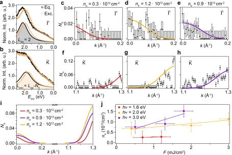
In order to determine the optically induced number of holes that accompanies the band
shifts, we apply an EDC-based analysis of the intensity loss in the VB introduced in Figure
4(a)-(b). As shown for EDCs around the ¯Γ (Figure 4a) and ¯K (Figure 4b) points for
the data in Figure 2d, we perform a fit with a Lorentzian on a linear background. The
background is allowed to vary for each momentum point due to tails from nearby graphene
bands, however, the background is held fixed as a function of time. The data taken before
the optical excitation are normalized such that the Lorentzian integrates up to the number
of electrons (2), which occupy a single momentum state in equilibrium. The integrated
Lorentzian after the optical excitation can then be used to determine the number of holes
in the k-range of the EDC. Applying this procedure for the data along ¯Γ- ¯K results in the
Leq = 2
Ebin (eV)
K
hν = 1.6 eV
hν = 2.0 eV
hν = 3.0 eV 2.0 1.0 0.0
3.0
2.0
1.0
0.0
2.0 1.0 0.0 Eq. Exc. 0.08 0.04 0.00 0.2
0.0 1.1 1.3
Γ
Norm. Int.
(arb. u.)
Nh
k (Å-1) F (mJ/cm2)
nh
(10
12/cm
2)
a
Lexc = Leq-Nh
nh = 0.9 ∙ 1012 cm-2
nh = 1.2 ∙ 1012 cm-2
nh = 0.3 ∙ 1012 cm-2
0.04 0.00 0.2 0.0 Nh 0.12 0.06 0.00 1.3 1.1 0.2 0.0 1.3 1.1 0.2 0.0 1.3 1.1
k (Å-1) k (Å-1) k (Å-1)
k (Å-1) k (Å-1) k (Å-1)
Nh 0.02 3.0 2.0 1.0 0.0 Norm. Int. (arb. u.)
nh = 0.3 ∙ 1012 cm-2 nh = 1.2 ∙ 1012 cm-2 nh = 0.9 ∙ 1012 cm-2
1.5 1.0 0.5 0.0 3 2 1 0 b
c d e
f g h
i j
Γ Γ Γ
[image:11.612.76.531.72.377.2]K K K
Figure 4: Analysis of optically induced hole density in the SL MoS2 layer: (a)-(b) EDCs
(markers) at ¯Γ and ¯K, plotted for a time delay before the optical excitation (black) and at peak excitation (orange) for the data in Figure 2d. Fits to a linear background and a single Lorentzian line shape are shown by lines and the Lorentzian parts are plotted individually.
The data are normalized such that the Lorentzian area Leq before excitation integrates up
to 2 electrons (Leq = 2, shown for ¯Γ in (a)). The number of generated holes in the state Nh
can then be determined from the Lorentzian area in the excited caseLexc byNh =Leq−Lexc
(shown for ¯K in (b)). (c)-(e) Hole profiles Nh(k) around ¯Γ and (f)-(h) around ¯K. The
markers are the experimental data obtained from the analysis in (a)-(b). Smooth curves are fits to a distribution function. (i) Fitted distribution functions from (c)-(h) shown for clarity. (j) Calculated hole density for SL MoS2 at peak excitation for different combinations
of pump energy and fluence. Lines through the data points have been added as a guide to the eye.
same pump pulse settings as the corresponding Figure 2c-e. The overall intensity loss in
the EDCs following excitation is comparable to the level of the noise, however, in the data
Nh is strongly peaked around the VB maxima at ¯Γ and ¯K at any given time and clearly
time resolution of 40 fs, leading to transient Fermi-Dirac like distributions near the band
extrema. Fits of such functions (see Figure S3c for an example of a raw fitting function)
to all data are shown in each panel of Figure 4c-h and combined in Figure 4i for ease of
comparison. The number of holes never exceeds 10% of the available states.
Because of the hole distribution’s strong energy dependence and the tendency to even an
anisotropic distribution out on a short time scale,29 it is reasonable to assume an isotropic
distribution around the local band maxima. The total hole densitynhin the VB can then be
calculated and the result is shown at peak excitation in Figure 4j. As expected, nh depends
on both the pump photon energy and fluence. The lines added to each set of points in
Figure 4j have been included as a guide to the eye to compare the overall magnitude and
trend of hole density with fluence for a given pump pulse energy. The excited hole density
is expected to extrapolate to zero and thus be a highly nonlinear function with fluence. A
complete understanding of this dependence is beyond the scope of this work. Furthermore,
a simple estimate using the pump pulse fluences and photon energies applied here would
lead to excited hole densities on the order of 1014−1015 cm−2 using the absorbance of 5-10 % for SL MoS2.30The much smaller hole densities we obtain are consistent with previous
TR-ARPES studies on graphene,18,22 and can be attributed to a combination of effects such
as Pauli blocking, recombination of carriers on faster timescales than we probe, diffusion of
excited carriers out of the probed area of the sample, as well as imperfect overlap of pump
and probe beams. Note that Figures 2 and 4 only provide values at peak excitation but
the energy shifts and hole densities are analyzed for entire sets of data with different delay
times between pump and probe pulse as shown in Figure S1i-j. This allows us to correlate
hole densities with the corresponding band gap reduction for a wide range of parameters and
conditions.
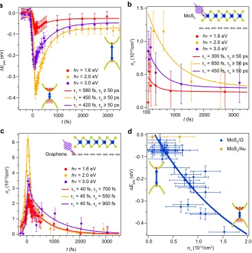
In Figure 5a we analyze the dynamical band gap reduction as a function of delay time
between the pump and probe pulse for the three data sets from Figure 2c-e. The largest
a b c d 100 -0.4 -0.3 -0.2 -0.1 0.0 3000 2000 1000 0 nh (10 12/cm 2) Δ Egap (eV)
t (fs) t (fs)
t (fs) ne
(10
12/cm 2)
nh (1012/cm2)
Δ Egap (eV) -0.4 -0.3 -0.2 -0.1 0.0 2.0 1.5 1.0 0.5 0.0
MoS2/G
MoS2/Au
6 5 4 3 2 1 0 3000 2000 1000 0
hν = 1.6 eV
hν = 2.0 eV
hν = 3.0 eV
τ1 = 40 fs, τ2 = 550 fs τ1 = 40 fs, τ2 = 700 fs
τ1 = 40 fs, τ2 = 900 fs
hν = 1.6 eV
hν = 2.0 eV
hν = 3.0 eV
τ1 = 450 fs, τ2 ≥ 50 ps τ1 = 580 fs, τ2 ≥ 50 ps
τ1 = 420 fs, τ2 ≥ 50 ps
1.5 1.0 0.5 0.0 3000 2000 1000
hν = 1.6 eV
hν = 2.0 eV
hν = 3.0 eV MoS2
Graphene
τ1 = 850 fs, τ2 ≥ 50 ps τ1 = 300 fs, τ2 ≥ 50 ps
[image:13.612.124.492.74.443.2]τ1 = 450 fs, τ2 ≥ 50 ps
Figure 5: Tuning the band gapvia optically induced carrier densities and substrate screening: (a) Time-dependent band gap renormalization for the data sets in Figure 2c-e. The lines correspond to an exponential rising edge followed by a double exponential decay with the decay time constants given in the figure. (b) Hole density as a function of delay time for the same data sets. Again, the two time constants for a double exponential decay are given. The time scale here begins at 100 fs because nh is undefined before the peak optical excitation
is reached. For the data after the peak excitation the time-delays have been binned over several time delay points. (c) Time-dependent hole density for the underlying graphene layer, extracted from the data sets in Figure 2f-h. The time constants for a double exponential
decay are given. (d) Plot of the total band gap renormalization versus the experimentally
extracted hole densities. A comparison with similar data obtained using a Au(111) substrate is included (Data from Ref. 9). The blue curve is merely a guide to the eye.
of 2 eV, which also has the highest fluence and results in the highest hole density at peak
(≈ 500 fs and ≈ 50 ps). Note that the time constant of 50 ps for the slow component is a lower estimate. Figure 5b shows the corresponding time dependence of the hole density.
A double exponential fit to these results in similar time constants but the uncertainties
on the individual data points are very large, even when wider ranges of time delays are
binned into a single data point. Nevertheless, the similar time constants strongly support
the interpretation that the observed band narrowing is induced by the excited carriers. The
presence of two characteristic decay times is also consistent with all-optical experiments.31
Figure 5c shows the time-dependent electron density in the graphene layer for the three
data sets shown in Figure 2f-h, illustrating that the carrier dynamics is entirely different from
the dynamics of the band gap reduction and hole density in the SL MoS2. Here a double
exponential fit results in a fast decay time that is more than an order of magnitude shorter
than that observed for SL MoS2. Since the optically induced electrons in graphene thermalize
within our time resolution, it is possible to estimate the transient electron density from the
electronic temperature. The extracted time-dependence of the electron density corresponds
well to that observed in previous experiments without the SL MoS2 on top.18,25Even though
we have regions of bare graphene within the probed area of the sample due to our MoS2
coverage of approximately 0.55 ML19 we also expect some signal from the graphene under
the MoS2.32 The observation of a single time constant suggests that the graphene dynamics
are at most weakly affected by the overlaid MoS2.
Finally, Figure 5d summarizes the key result of this paper, the band gap shrinkage as
a function of excited hole density, combining data taken with different excitation energies
and fluences. These results can be compared to a recent prediction by Steinhoff et al. which
gives a somewhat larger shrinkage but with the same order of magnitude as observed here
(≈0.5 eV for a carrier density of≈ 1012 cm−2).5 The discrepancy between experiment and
theory can easily be accounted for by the uncertainties in the determination of the carrier
concentration and the role of the underlying graphene, which is not present in the calculation.
MoS2on SiO2, either by optical or electrical doping6,7and for surface doping of bulk WSe2.33
However, the effect is nearly completely suppressed when MoS2 is placed in a strongly
screen-ing environment such as on a metallic Au(111) substrate.9,10To illustrate this, we have added
the result of a corresponding analysis, using data for MoS2/Au(111) from Ref. 9. In this case
(orange data points in Figure 5d) the band shift remains below 10 meV, even for high induced
carrier densities. Also, the typical decay times for excited carriers (≈50 fs) are much faster than observed here or for MoS2 on SiO2.6,31Our results are reminiscent of TR-ARPES
stud-ies on the strongly correlated metallic TMDC 1T-TiSe2.34,35 This system exhibits a charge
ordered state, which is completely removed due to additional screening from optically excited
free carriers.34 This scenario is consistent with our interpretation of a band gap reduction in
SL MoS2 due to the build-up of screening via laser-induced free carriers.
Conclusion
As our results show, the static screening of charge carriers in SL MoS2 in a heterostructure
with graphene is sufficiently weak that a significant band gap renormalization can be induced
by optically excited carriers. On a fundamental level, this suggests that the degree of control
of the electronic structure of such heterostructures extends beyond the substrate-induced
renormalization of the static band gap of the 2D semiconductor to the dynamic tuneability
of the band gap and the electron dynamics. This behavior is essential to take into account
in optical applications where the change of the resonance condition on ultrafast time scales
may pose a serious challenge, e.g. in the design of an actual optical cavity. On the other
hand, one could imagine optoelectronic devices based on a heterostructure with different
band alignments in the constituent materials where ultrafast light-induced switching of the
band offsets could be used as a means to control the separation of excitons and free charge
Materials and Methods
Sample preparation
The MoS2/G heterostructure was synthesized on a 6H-SiC 2 in. wafer (TanKeBlue
Semicon-ductor Co. Ltd., n-type doping, 0.02-0.10 Ω·cm). The epitaxial graphene layer was grown
first on the Si terminated (0001) face by direct current annealing of the 6H-SiC substrate
in a dedicated ultra-high vacuum (UHV) graphene growth chamber with a base pressure of
5×10⁻¹⁰ mbar. The dangling Si bonds of the substrate were saturated by a carbon buffer
layer with a (6√3×6√3)R30◦ periodicity under the graphene layer. MoS2 was then grown
on top of the graphene by van der Waals epitaxy in a separate UHV chamber. In this
proce-dure the Mo was initially deposited from an electron beam evaporator (Oxford Instruments)
in a H2S atmosphere of ≈ 1×10⁻⁵ mbar. After deposition the sample was annealed for
≈1 hour at 1050 K in the H2S environment, which resulted in nanosized islands of MoS2 on
the graphene. Repeated cycles of this process lead to the formation of a SL MoS2 film with
an optimum coverage around 0.55 ML before bilayer MoS2 islands nucleated, as determined
by scanning tunneling microscopy. Further details on the growth are provided in Ref. 19.
ARPES
The equilibrium electronic structure of the MoS2/G sample was determined by ARPES at
the SGM-3 UHV end-station of the synchrotron radiation source ASTRID2 in Aarhus,
Den-mark.36The sample was initially annealed to 500 K to remove adsorbed species. The ARPES
data was collected at a photon energy of 70 eV over a significant portion of the MoS2 and
graphene Brillouin zones (BZs) in order to determine the location of the band extrema of
the two materials and their relative orientation with respect to each other. This information
was used to align the sample in the TR-ARPES experiments. The sample temperature was
respectively.
TR-ARPES
The same sample that was measured by ARPES was then transported in an evacuated
tube pumped down below 1 × 10⁻⁹ mbar to the Artemis facility, Rutherford Appleton
Laboratory in Harwell, UK for TR-ARPES measurements.37 Here it was placed in the
TR-ARPES UHV end-station and annealed to 500 K in order to remove any adsorbed surface
contaminants. The sample temperature was kept at 50 K using a liquid helium cryostat
during measurements.
The pump and probe pulses used for acquiring TR-ARPES spectra were generated using
a 1 kHz Ti:sapphire amplified laser system with a wavelength of 785 nm, a pulse duration
of 30 fs and an energy per pulse of 12 mJ. The band structures of MoS2 and graphene
were measured along their ¯Γ- ¯K directions using high harmonic probe pulses of hν = 25 eV,
which were generated by focusing a part of the laser energy on a pulsed jet of argon gas.
The remaining laser energy was applied to drive an optical parametric amplifier (HE-Topas)
followed by a frequency mixing stage. This provided tunable pump pulses with wavelengths
centered at 408 nm (3.0 eV), 615 nm (2.0 eV) and 784 nm (1.6 eV), which were used
to optically excite the sample. The fluence of the pump pulse was kept in the range
0.4-3.0 mJ/cm2, and the maximum used for any of the three applied wavelengths was kept below
the onset where significant energy broadening and shifts of the measured spectra started to
occur due to pump-induced space-charge effects.26 The beams were polarized such that the
pump pulse wass-polarized and the probe pulse was p-polarized.
The time delays of pump and probe pulses were varied using a mechanical delay line. We
applied two modes of acquisition: (1) A few-delay-point mode where we measured the spectra
over 3-6 time delay points around peak optical excitation but acquired these cumulatively
where we measured the spectra over 50-60 time delay points cumulatively up to 1000 times.
Acquisition times of the few-delay-point mode were up to 3 h, which enabled us to acquire
data at 3-4 different pump fluence settings per pump wavelength. In the many-delay-point
mode acquisition times were up to 20 h per dataset, which limited the number of experimental
parameters that we could vary in such experiments, but allowed us to capture the detailed
time dependence. Throughout this work we have defined t= 0 to coincide with the middle
of the rising edge in the measured spectra following optical excitation of the sample. The
energy-, angular- and time-resolution were 400 meV, 0.3◦ and 40 fs, respectively.
Acknowledgement
We thank Phil Rice for technical support during the Artemis beamtime. We gratefully
ac-knowledge funding from the VILLUM foundation, the Lundbeck foundation, EPSRC (Grant
Nos. EP/I031014/1 and EP/L505079/1), The Royal Society and the Swiss National
Sci-ence Foundation (NSF). Ph. H. and S. U. acknowledge financial support from the Danish
Council for Independent Research, Natural Sciences under the Sapere Aude program (Grant
Nos. DFF-4002-00029 and DFF-4090-00125). Access to the Artemis Facility was funded by
STFC.
Supporting Information Available
Supporting online information is available with details on the analysis of band shifts,
conduc-tion band posiconduc-tion, MoS2 hole density calculation and graphene electron density calculation.
This material is available free of charge via the Internet at http://pubs.acs.org/.
References
2. Georgiou, T.; Jalil, R.; Belle, B. D.; Britnell, L.; Gorbachev, R. V.; Morozov, S. V.;
Kim, Y.-J.; Gholinia, A.; Haigh, S. J.; Makarovsky, O.; Eaves, L.; Ponomarenko, L. A.;
Geim, A. K.; Novoselov, K. S.; Mishchenko, A. Vertical Field-Effect Transistor Based
on Graphene-WS2 Heterostructures for Flexible and Transparent Electronics.Nat.
Nan-otechnol. 2013, 8, 100.
3. Roy, K.; Padmanabhan, M.; Goswami, S.; Sai, T. P.; Ramalingam, G.; Raghavan, S.;
Ghosh, A. Graphene-MoS2Hybrid Structures for Multifunctional Photoresponsive
Mem-ory Devices. Nat. Nanotechnol.2013, 8, 826.
4. Ugeda, M. M.; Bradley, A. J.; Shi, S.-F.; da Jornade, F. H.; Zhang, Y.; Qiu, D. Y.;
Ruan, W.; Mo, S.-K.; Hussain, Z.; Shen, Z.-X.; Wang, F.; Louie, S. G.; Crommie, M. F.
Giant Bandgap Renormalization and Excitonic Effects in a Monolayer Transition Metal
Dichalcogenide Semiconductor. Nat. Mater. 2014, 13, 1091.
5. Steinhoff, A.; R¨osner, M.; Jahnke, F.; Wehling, T. O.; Gies, C. Influence of Excited
Carriers on the Optical and Electronic Properties of MoS2. Nano Lett. 2014,14, 3743.
6. Chernikov, A.; Ruppert, C.; Hill, H. M.; Rigosi, A. F.; Heinz, T. F. Population Inversion
and Giant Bandgap Renormalization in Atomically Thin WS2 Layers. Nat. Photonics
2015,9, 466.
7. Chernikov, A.; van der Zande, A. M.; Hill, H. M.; Rigosi, A. F.; Velauthapillai, A.;
Hone, J.; Heinz, T. F. Electrical Tuning of Exciton Binding Energies in Monolayer WS2.
Phys. Rev. Lett. 2015,115, 126802.
8. Pogna, E. A. A.; Marsili, M.; Fazio, D. D.; Conte, S. D.; Manzoni, C.; Sangalli, D.;
Yoon, D.; Lombardo, A.; Ferrari, A. C.; Marini, A.; Cerullo, G.; Prezzi, D. Photo-Induced
Bandgap Renormalization Governs the Ultrafast Response of Single-Layer MoS2. ACS
9. Grubiˇsi´c ˇCabo, A.; Miwa, J. A.; Grønborg, S. S.; Riley, J. M.; Johannsen, J. C.;
Ca-cho, C.; Alexander, O.; Chapman, R. T.; Springate, E.; Grioni, M.; Lauritsen, J. V.;
King, P. D. C.; Hofmann, P.; Ulstrup, S. Observation of Ultrafast Free Carrier Dynamics
in Single Layer MoS2.Nano Lett. 2015, 15, 5883.
10. Bruix, A.; Miwa, J. A.; Hauptmann, N.; Wegner, D.; Ulstrup, S.; Grønborg, S. S.;
Sanders, C. E.; Dendzik, M.; Grubiˇsi´c ˇCabo, A.; Bianchi, M.; Lauritsen, J. V.;
Khaje-toorians, A. A.; Hammer, B.; Hofmann, P. Single-Layer MoS2 on Au(111): Band Gap
Renormalization and Substrate Interaction. Phys. Rev. B 2016, 93, 165422.
11. Mak, K.; Lee, C.; Hone, J.; Shan, J.; Heinz, T. Atomically Thin MoS2: A New
Direct-Gap Semiconductor. Phys. Rev. Lett. 2010,105, 136805.
12. Splendiani, A.; Sun, L.; Zhang, Y.; Li, T.; Kim, J.; Chim, C.-Y.; Galli, G.; Wang, F.
Emerging Photoluminescence in Monolayer MoS2. Nano Lett. 2010, 10, 1271.
13. Qiu, D. Y.; da Jornada, F. H.; Louie, S. G. Optical Spectrum of MoS2: Many-Body
Effects and Diversity of Exciton States. Phys. Rev. Lett. 2013, 111, 216805.
14. Kalt, H.; Rinker, M. Band-Gap Renormalization in Semiconductors with Multiple
In-equivalent Valleys. Phys. Rev. B 1992, 45, 1139.
15. Tr¨ankle, G.; Leier, H.; Forchel, A.; Haug, H.; Ell, C.; Weimann, G. Dimensionality
Dependence of the Band-Gap Renormalization in Two- and Three-Dimensional
Electron-Hole Plasmas in GaAs. Phys. Rev. Lett. 1987,58, 419.
16. Das Sarma, S.; Jalabert, R.; Yang, S.-R. E. Band-Gap Renormalization in Semiconductor
Quantum Wells. Phys. Rev. B 1990, 41, 8288.
17. Jin, C.; Rasmussen, F. A.; Thygesen, K. S. Tuning the Schottky Barrier at the
Graphene/MoS2 Interface by Electron Doping: Density Functional Theory and
18. Johannsen, J. C.; Ulstrup, S.; Crepaldi, A.; Cilento, F.; Zacchigna, M.; Miwa, J. A.;
Ca-cho, C.; Chapman, R. T.; Springate, E.; Fromm, F; Raidel, C.; Seyller, T.; King, P. D. C.;
Parmigiani, F.; Grioni, M.; Hofmann, P. Tunable Carrier Multiplication and Cooling in
Graphene. Nano Lett. 2015,15, 326.
19. Miwa, J. A.; Dendzik, M.; Grønborg, S. S.; Bianchi, M.; Lauritsen, J. V.; Hofmann, P.;
Ulstrup, S. Van der Waals Epitaxy of Two-Dimensional MoS2-Graphene
Heterostruc-tures in Ultrahigh Vacuum. ACS Nano 2015,9, 6502.
20. Bostwick, A.; Ohta, T.; Seyller, T.; Horn, K.; Rotenberg, E. Quasiparticle Dynamics in
Graphene. Nat. Phys. 2007, 3, 36.
21. H¨user, F.; Olsen, T.; Thygesen, K. S. How Dielectric Screening in Two-Dimensional
Crystals Affects the Convergence of Excited-State Calculations: Monolayer MoS2.Phys.
Rev. B 2013, 88, 245309.
22. Johannsen, J. C.; Ulstrup, S.; Cilento, F.; Crepaldi, A.; Zacchigna, M.; Cacho, C.;
Turcu, I. C. E.; Springate, E.; Fromm, F.; Raidel, C.; Seyller, T.; Parmigiani, F.;
Grioni, M.; Hofmann, P. Direct View of Hot Carrier Dynamics in Graphene. Phys. Rev.
Lett. 2013,111, 027403.
23. Gierz, I.; Petersen, J. C.; Mitrano, M.; Cacho, C.; Turcu, I. C. E.; Springate, E.;
St¨ohr, A.; K¨ohler, A.; Starke, U.; Cavalleri, A. Snapshots of Non-Equilibrium Dirac
Carrier Distributions in Graphene. Nat. Mater. 2013,12, 1119.
24. Ulstrup, S.; Johannsen, J. C.; Cilento, F.; Miwa, J. A.; Crepaldi, A.; Zacchigna, M.;
Cacho, C.; Chapman, R. T.; Springate, E.; Mammadov, S.; Fromm, F.; Raidel, C.;
Seyller, T.; Parmigiani, F.; Grioni, M.; King, P. D. C.; Hofmann, P. Ultrafast Dynamics
of Massive Dirac Fermions in Bilayer Graphene. Phys. Rev. Lett. 2014, 112, 257401.
Itatani, J.; Komori, F.; Shin, S.; Matsuda, I. Observing Hot Carrier Distribution in an
n-Type Epitaxial Graphene on a SiC Substrate. Appl. Phys. Lett.2014, 104, 161103.
26. Ulstrup, S.; Johannsen, J. C.; Cilento, F.; Crepaldi, A.; Miwa, J. A.; Zacchigna, M.;
Cacho, C.; Chapman, R. T.; Springate, E.; Fromm, F.; Raidel, C.; Seyller, T.;
King, P. D. C.; Parmigiani, F.; Grioni, M.; Hofmann, P. Ramifications of Optical
Pump-ing on the Interpretation of Time-Resolved Photoemission Experiments on Graphene.
J. Electron Spectrosc. Relat. Phenom. 2015, 200, 340.
27. Yang, S.-L.; Sobota, J.; Kirchmann, P.; Shen, Z.-X. Electron Propagation from a
Photo-Excited Surface: Implications for Time-Resolved Photoemission. Appl. Phys. A: Mater.
Sci. Process. 2014, 116, 85–90.
28. Tanaka, S. Utility and Constraint on the use of Pump-Probe Photoelectron Spectroscopy
for Detecting Time-Resolved Surface Photovoltage. J. Electron Spectrosc. Relat.
Phe-nom. 2012, 185, 152 – 158.
29. Mittendorff, M.; Winzer, T.; Malic, E.; Knorr, A.; Berger, C.; de Heer, W. A.;
Schnei-der, H.; Helm, M.; Winnerl, S. Anisotropy of Excitation and Relaxation of
Photogener-ated Charge Carriers in Graphene. Nano Lett. 2014, 14, 1504.
30. Bernardi, M.; Palummo, M.; Grossman, J. C. Extraordinary Sunlight Absorption and
One Nanometer Thick Photovoltaics using Two-Dimensional Monolayer Materials.Nano
Lett. 2013,13, 3664–3670.
31. Wang, H.; Zhang, C.; Rana, F. Ultrafast Dynamics of Defect-Assisted Electron–Hole
Recombination in Monolayer MoS2. Nano Lett. 2015, 15, 339.
32. Zhang, Y.; Chang, T.; Zhou, B.; Cui, Y.; Yan, H.; Liu, Z.; Schmitt, F.; Lee, J.; Moore, R.;
Chen, Y.; Lin, H.; Jeng, H.-T.; Mo, S.-K.; Hussain, Z.; Bansil, A.; Shen, Z. X. Direct
Ob-servation of the Transition from Indirect to Direct Bandgap in Atomically Thin Epitaxial
33. Riley, J. M.; Meevasana, W.; Bawden, L.; Asakawa, M.; Takayama, T.; Eknapakul, T.;
Kim, T. K.; Hoesch, M.; Mo, S. K.; Takagi, H.; Sasagawa, T.; Bahramy, M. S.;
King, P. D. C. Negative Electronic Compressibility and Tunable Spin Splitting in WSe2.
Nat. Nanotechnol. 2015, 10, 1043.
34. Rohwer, T.; Hellmann, S.; Wiesenmayer, M.; Sohrt, C.; Stange, A.; Slomski, B.; Carr, A.;
Liu, Y.; Avila, L. M.; Kallane, M.; Mathias, S.; Kipp, L.; Rossnagel, K.; Bauer, M.
Collapse of Long-Range Charge Order Tracked by Time-Resolved Photoemission at High
Momenta. Nature 2011, 471, 490–493.
35. Hellmann, S.; Rohwer, M.; Kall¨ane, M.; Hanff, K.; Sohrt, C.; Stange, A.; Carr, A.;
Murnane, M. M.; Kapteyn, H. C.; Kipp, L.; Bauer, M.; Rossnagel, K. Time-Domain
Classification of Charge-Density-Wave Insulators. Nat. Commun. 2012, 3, 1069.
36. Hoffmann, S. V.; Søndergaard, C.; Schultz, C.; Li, Z.; Hofmann, P. An
Undulator-Based Spherical Grating Monochromator Beamline for Angle-Resolved Photoemission
Spectroscopy. Nucl. Instrum. Methods Phys. Res., Sect. A 2004, 523, 441.
37. Frassetto, F.; Cacho, C.; Froud, C. A.; Turcu, I. C. E.; Villoresi, P.; Bryan, W. A.;
Springate, E.; Poletto, L. Single-Grating Monochromator for Extreme-Ultraviolet