DESIGN AND IMPLEMENTATION OF A TRANSCEIVERON A MODEL BASED DEVELOPMENT
PLATFORM USING SAMPLED MATCH FILTER DETECTIONFOR SOFTWARE
Department of Electronics Engineering
ARTICLE INFO ABSTRACT
Software
communication standards.
describes the implementation of QAM
detection technique. The advantage of using sampled matched filter is maximizing the signal
ratio (SNR) at the output of the matched filter. The Transceiver also uses Forward Error Correction (FEC) in the form of Reed
based development platform for Software Defined Radio. The whole system consists of a Front or DSP model and a Back
configurability and the complete base
the front end is generated in C VHDL.
Copyright © 2018, Rehan Muzammil. This is an open access distribution, and reproduction in any medium, provided
INTRODUCTION
SDR has the ability of changing the characteristics of a transmitting and receiving radio device without physically modifying the hardware. Presently a number of communication standards are commercially available which comes under 2G, 3G and now 4G technologies. The present technologies oblige their users to buy a particular device for each type of communication standard, and operators have to deploy base stations for each system. The circumstances are such that users are required to switch from one standard to another very frequently. For this case, emerging multi
bands, multi-modes and multi-protocol systems have been developed. Thus, SDR can serve as the fundamental technology where all these systems can be implemented in one hardware platform. SDR allows system
re-reprogramming by using software commands. The work of the SDR includes hardware adaptability by software means. Thus SDR is one possible way to realize the structure of the device with mobility, flexibility, and re-configurability
2008). In response to a myriad of communication standards currently available, radio designers are architecting SDR systems that have the ability to support present and future waveform specifications. Such system facilitate
of new waveform components by offering standardized interfaces to which waveform components connect (Noseworthy, 2007).
*Corresponding author: Rehan Muzammil
Department of Electronics Engineering, Aligarh Muslim University, Aligarh, India
ISSN: 0975-833X
Vol. 10, Issue,
Article History:
Received 15th September, 2018 Received in revised form 04th October, 2018
Accepted 19th November, 2018 Published online 29th December, 2018
Citation: Rehan Muzammil. 2018. “Design and implementation of a transceiveron a model based development platform using sampled match filter detectionfor software defined radio”, International Journal of Current Research
Key Words:
SDR, Matched Filter, VHDL, DSP, FPGA, Reed-Solomon.
RESEARCH ARTICLE
DESIGN AND IMPLEMENTATION OF A TRANSCEIVERON A MODEL BASED DEVELOPMENT
PLATFORM USING SAMPLED MATCH FILTER DETECTIONFOR SOFTWARE
*Rehan Muzammil
Department of Electronics Engineering, Aligarh Muslim University
ABSTRACT
Software defined radio (SDR) seems to be a solution for communications for rapid changes in the communication standards. Detector is the most important component of radio receiver. This paper describes the implementation of QAM-4 transceiver using very simple sample
detection technique. The advantage of using sampled matched filter is maximizing the signal
ratio (SNR) at the output of the matched filter. The Transceiver also uses Forward Error Correction (FEC) in the form of Reed-Solomon (7, 3) coding and decoding. This design is tested using a model based development platform for Software Defined Radio. The whole system consists of a Front or DSP model and a Back-End or FPGA model. FPGAs are chosen due to their high re
figurability and design flexibility when compared with Digital Signal Processors. Because of this the complete base-band processing of the transceiver is performed at the FPGA model. The coding for the front end is generated in C-language whereas the coding for the Back
VHDL.
access article distributed under the Creative Commons Attribution the original work is properly cited.
SDR has the ability of changing the characteristics of a transmitting and receiving radio device without physically modifying the hardware. Presently a number of communication standards are commercially available which comes under 2G, ogies. The present technologies oblige their users to buy a particular device for each type of communication standard, and operators have to deploy base stations for each system. The circumstances are such that users rd to another very frequently. For this case, emerging standards,
multi-protocol systems have been developed. Thus, SDR can serve as the fundamental technology where all these systems can be implemented in one -configuration and reprogramming by using software commands. The work of the SDR includes hardware adaptability by software means. Thus SDR is one possible way to realize the structure of the device configurability (Zlydareva . In response to a myriad of communication standards currently available, radio designers are architecting SDR systems that have the ability to support present and future waveform specifications. Such system facilitate the integration of new waveform components by offering standardized interfaces to which waveform components connect
Department of Electronics Engineering, Aligarh Muslim University, Aligarh,
To avoid costly upgrades or total communications receiver / processor device replacement due to sometimes rapidly changing wireless communications protocols and standards, J. Mitola proposed the concept of SDR in 1995. In SDR, most radio receiver/processing functions would be defined by user written software programs, to be run on general purpose (GP) programmable processor rather than the functions being implemented strictly in non-programmable hardware
2010).The traditional SDR platform for di
mainly based on General Purpose Processors (GPPs) and Digital Signal Processors (DSPs) which are adequate for future high data rate wireless communications in terms of processing speed and energy efficiency (Qiwei Zhang
the software SDR concept is emerging as a potential pragmatic solution. The solution is to enable the operators to reuse their existing infrastructure and sites to support the various air interface standards using single base station architectu make a very flexible use of multiple frequency bands and multiple standards using common hardware
SDR is one where the baseband processing is carried on programmable and /or reconfigurable hardware to achieve flexibility. SDR applications typically expose lots of data level parallelism. This parallelism can be directly tracked by the programmer through intrinsic functions
operates under different standards (GSM, IS For this reason SDR uses a combina
include multi-band antennas and RF conversion; wideband ADC; DAC; and implementation of IF
wireless receivers, the complete implementation of the SDR
International Journal of Current Research
Vol. 10, Issue, 12, pp.75944-75953, December, 2018
DOI: https://doi.org/10.24941/ijcr.33448.12.2018
Design and implementation of a transceiveron a model based development platform using sampled match filter
International Journal of Current Research, 10, (12), 75944-75953.
DESIGN AND IMPLEMENTATION OF A TRANSCEIVERON A MODEL BASED DEVELOPMENT
PLATFORM USING SAMPLED MATCH FILTER DETECTIONFOR SOFTWARE DEFINED RADIO
Aligarh Muslim University, Aligarh, India
fined radio (SDR) seems to be a solution for communications for rapid changes in the Detector is the most important component of radio receiver. This paper 4 transceiver using very simple sampled matched filter detection technique. The advantage of using sampled matched filter is maximizing the signal-to-noise ratio (SNR) at the output of the matched filter. The Transceiver also uses Forward Error Correction 3) coding and decoding. This design is tested using a model based development platform for Software Defined Radio. The whole system consists of a Front-End End or FPGA model. FPGAs are chosen due to their high re-flexibility when compared with Digital Signal Processors. Because of this band processing of the transceiver is performed at the FPGA model. The coding for language whereas the coding for the Back-End model is generated in
License, which permits unrestricted use,
To avoid costly upgrades or total communications receiver / processor device replacement due to sometimes rapidly changing wireless communications protocols and standards, J. Mitola proposed the concept of SDR in 1995. In SDR, most sing functions would be defined by user written software programs, to be run on general purpose (GP) programmable processor rather than the functions being programmable hardware (Alluri, The traditional SDR platform for digital processing is mainly based on General Purpose Processors (GPPs) and Digital Signal Processors (DSPs) which are adequate for future high data rate wireless communications in terms of processing Qiwei Zhang, 2007). Therefore, the software SDR concept is emerging as a potential pragmatic solution. The solution is to enable the operators to reuse their existing infrastructure and sites to support the various air interface standards using single base station architecture to make a very flexible use of multiple frequency bands and multiple standards using common hardware (Mohamed, 2007). SDR is one where the baseband processing is carried on programmable and /or reconfigurable hardware to achieve tions typically expose lots of data level parallelism. This parallelism can be directly tracked by the programmer through intrinsic functions (Schuster, 2006). SDR operates under different standards (GSM, IS-95, UMTS,….). For this reason SDR uses a combination of techniques that band antennas and RF conversion; wideband ADC; DAC; and implementation of IF (Mohamed, 2007). In wireless receivers, the complete implementation of the SDR
OF CURRENT RESEARCH
concept is mainly limited by the analog front-end. In the task of down-converting the bandpass signal to baseband, or at least to low frequencies, front-ends are usually limited to certain frequency band and power level. The increasing set of wireless standards has encouraged researchers to look further into digital techniques for down-conversion process (Rodriguez-Pareram, 2017). RS codes have practical advantages over the other codes in terms of memory size and decoder complexity. An exact analytical form for the error probability is available for RS codes. This is useful for obtaining the optimal code rates and the optimal power allocation (Banani, 2011).
The ideal architecture for SDR involves placement of analog to digital converter immediately after the antenna, resulting in performing all the tasks ranging from RF processing to Baseband processing in software. As the evolution of ADCs do not pace up with Moore’s law and power dissipation of ADCs at Radio Frequencies is very high, an ideal SDR becomes unrealizable. Hence, a software Radio architecture comprising of Radio Frequency (RF) stage, Intermediate Frequency (IF) stage and Baseband processing stage is a near solution to ideal SDR (Agarwal, 2014). An SDR is a communications platform that uses software for fast prototyping of digital communications algorithms, while allowing analog transmissions over a physical medium (Politis, 2018). The greatest advantage of SDRs is the reduction in size, cost and power consumption, since data processing can be usually performed in a single device. Unfortunately, most of those systems are limited to a specific frequency band, since the specific requirements of each application are mainly related to RF properties (down-/up conversion, RF bandwidth and signal strength) and the analog-digital conversion (Budroweit, 2018). In this paper RS (7, 3) coding and decoding has been used in the design of the transceiver. No interleaving and de-interleaving blocks are used because of the RS codes are used for burst errors. In this paper sampled matched filter detection at the receiver is used which maximizes the signal to noise ratio at the front end of the receiver.
The QAM-4 modulation and demodulation scheme is used in the design of the transceiver. The whole transceiver is designed, implemented and tested on a model based development platform for Software Defined Radio. This paper is organized as follows. The first section is the introduction. Section 2 describes model based development platform. Section 3 describes the RS (7, 3) coding and decoding technique used in this work. Section 4 gives an overview of the Front-end model for this transceiver. Section 5 gives an overview of the Back-end model for this transceiver. Section 6 describes the sampled matched filter detection technique. Section 7 gives the Simulation results. Section 8 gives the real time results. Section 9 gives the conclusion.
Model Based Development
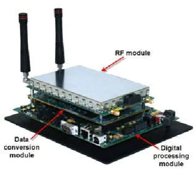
[image:2.595.334.533.50.225.2]In this work, the authors have used a Model Based Development platform. This is a Small Form factor (SFF) SDR low power tunable equipment manufactured by Lyrtech, Canada. This SFF SDR platform is conceived and designed to be used in the development of applications in the field of Software Defined Radio and is composed of three boards: RF module, Data Conversion Module, Data Processing Module. The board is illustrated in the Fig. 1.
Figure 1. The SFF SDR platform
The SFF SDR platform comes with two board support packages – Board Software Development Kit (BSDK) and Model Based Development kit (MBDK). The BSDK allows users to quickly become fully functional developing C, C++, or assembly language codes for the DSP and GPP, or HDL code for the FPGA by giving users an understanding of all the platform’s major interfaces such as VPSS, audio codec, data conversion module, or RF module. Similarly, the MBDK allows users to develop applications for the platform with Simulink within MATLAB. By targeting the DSP and FPGA with MBDK tools, users can deploy and validate algorithms on the hardware more rapidly. Unlike the SDR development platforms on the market, the SFF SDR development platform is a hybrid hardware-software system that supplies the necessary full signal chain for multi-protocol software defined radios. By separating the base-band, IF, and RF from one another as distinct modules (rather than maintaining a single, fixed architecture), developers can extend their radio development capabilities and optimize costs and power consumption. The SFF SDR development platforms can be used to perform four types of development – FPGA, DSP, GPP, and Model based (combination of the above three). This paper describes model based development using this platform, though only FPGA and DSP are exploited.
(7, 3) Reed-Solomon Coding and Decoding (Sklar 2013):
The Reed-Solomon coding and decoding is realized with the help of VHDL codes. Both the RS coder and decoder are designed and implemented using VHDL. Reed-Solomon codes are non-binary cyclic codes with symbols made up of m-bit sequences, where m is positive integer having a value greater than 2. R-S (n,k) codes on m-bit symbols exist for all n and k for which,
0 < < < 2 + 2 ……….… (1)
Where k is the number of data symbols being encoded, and n is the total number of code symbols in the encoded block. For the most conventional R-S (n, k) code [10],
( , ) = (2 − 1, 2 − 1 − 2 ) ……….… (2)
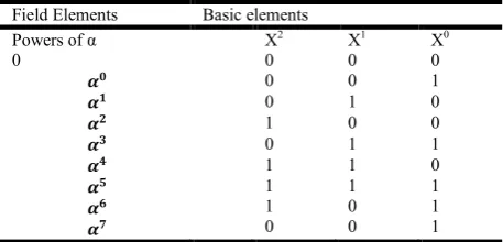
added to make it 7 symbols code-word. Hence, R-S (7, 3) coding is realized. The algorithm for generating the additional 4-symbols of parity is described in the following paragraphs. In order to understand the encoding and decoding of the R-S codes, it is necessary to venture into the area of finite fields known as Galois Fields (GF). For any prime number, p, there exists a finite field denoted GF (p) that contains p elements. Here p = 2m which can be represented by a power of α. An infinite set of elements, F, is formed by starting with elements {0, 1, α}, and generating the additional elements by progressively multiplying the last entry by α, which yields the following [10, Bernard-Sklar book]:
= {0,1, , , … … . } ……….… (3)
Here a finite set of elements of GF (2m) is formed from F. In this application m=3 hence there should be 8 elements in F. A class of polynomials called primitive polynomials is of interest because such functions define the finite fields GF (2m) that is needed to define RS codes. Here in this case the bits per symbol are 3 hence the primitive polynomial is:
1 + + = 0 ……… (4)
Putting x = α and rearranging we get,
−1 − = ……….… (5)
Since in binary filed -1 = +1 we can write,
1 + = ……….… (6)
From Equation 6 we can derive all the elements of GF (2m) which are:
{0, , , , , , , }
Reed-Solomon Coding
The symbols are depicted in the Table 1.
[image:3.595.48.277.562.672.2]The multiplication table is given in Table 2for m=3 and primitive polynomial 1+x+x3 (all values are powers of α). The addition table is given in Table 3:
Table 1. Symbols Table
Field Elements Basic elements
Powers of α X2 X1 X0
0 0 0 0
0 0 1 0 1 0 1 0 0 0 1 1 1 1 0 1
1 0
1 0 0
[image:3.595.64.261.706.786.2]1 1 1
Table 2. Multiplication Table (Numbers signify powers of α)
0 1 2 3 4 5 6 0 0 1 2 3 4 5 6 1 1 2 3 4 5 6 0 2 2 3 4 5 6 0 1 3 3 4 5 6 0 1 2 4 4 5 6 0 1 2 3 5 5 6 0 1 2 3 4 6 6 0 1 2 3 4 5
Table 3. Addition Table (Numbers signify powers of α)
0 1 2 3 4 5 6 0 Zero 3 6 1 5 4 2 1 3 Zero 4 0 2 6 5 2 6 4 Zero 5 1 3 0 3 1 0 5 Zero 6 2 4 4 5 2 1 6 Zero 0 3 5 4 6 3 2 0 Zero 1 6 2 5 0 4 3 1 Zero
It may be emphasized here that all the values in the above tables depict powers of α except for “Zero” which means zero.
Next step is to find the generator polynomial which is given as:
( ) = + + + + ⋯ + +
……….… (7)
The degree of generator polynomial is equal to the number of parity symbols. We describe the generator polynomial in terms of its 2t = n-k = 4 roots, as follows:
( ) = ( − )( − ) … . . ( − )……….… (8)
Equation (8) can be simplified using Table 3& 4 and using modulo 2 additions. All the negative signs are converted into positive signs. We get,
( ) = + + + + ……… (9)
Next we find out the parity polynomial which is given as,
( ) = ( ) ( ) ………(10)
Where m(X) is the message polynomial and (n-k) = 4. Hence, the code-word becomes:
( ) = ( ) + ( ) …………..… (11)
Reed-Solomon Decoding
Error is introduced into the code-word after the code-word is transmitted over a channel, e(X). Hence, the received code polynomial is,
( ) = ( ) + ( ) ………...(12)
To remove the errors, maximum 2 symbols or 6 bits in 7 symbols or 21 bits of code-word, syndrome is calculated which is given as,
= ( )| = ( ) …………..….(13)
Where i = 1, …, (n-k). Hence, there are 4 syndrome values calculated using the Equation (13) and Table 3& 4. If all the syndrome values are zero it signifies that there is no error. If some of the values of syndrome is non zero signifies there is error.Next step is to find the error location. The error locator polynomial σ(X) can be described as follows:
( ) = (1 + )(1 + ) … (1 + ) …………(14)
( ) = 1 + + + ⋯ + …………(15)
= ………..(16)
Next we find the inverse of the matrix on the left hand side. If the determinant is zero it signifies 1 symbol error. Then we are left with S1. If S1 is zero signifies that there is more than 2 symbol errors. Hence, if there are more than 2 symbol errors it cannot be corrected as there is no way of finding and correcting more than 2 symbol errors in RS (7, 3) codes.Once we find out the value of σ1, σ2, from Equation (16), we can write,
( ) = 1 + + …….……..… (17)
From Equation (17) we can find out the error locations as,
( ) = 1 + ( ) + ( ) ……….…(18)
Where, i = 0, 1, 2, …,6.
From the values obtained in Equation (18) we can say that wherever the value of σ(αi) is zero, there is an error. Now at this stage we have found out the error locations. Next step is to find out the error values which is calculated as,
= ( ) = + ...………(19)
= ( ) = + ……….(20)
It can be written in matrix form as,
= …………...…(21)
For finding the value of e1, e2 we first find the inverse of the matrix on the left hand side. Once we get these values we next go in for the symbol error correction. It may be emphasized here that R-S codes does whole symbol correction whether there is single bit error in the symbol or multiple bit errors. The values of these error codes are modulo 2 added with the symbols at the corresponding locations which remove the errors.
̂( ) = + ……….…(22)
Where j1, j2 are the error locations.
( ) = ( ) + ̂( ) = ( ) + ( ) + ̂( ) ……...… (23)
The whole process is performed for 2-symbol or 1-symbol errors in the same fashion. Thus if the error and estimate of error are the same, they cancel out and we get the original transmitted code-word.
Front-End Model of the Transceiver
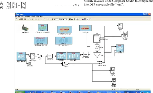
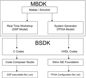
The front-end model of the transceiver is the one where the controls of DAC, ADC, and RF resides. There is line-in jack on the data processing module of the platform where the mp3 player is plugged in. The received audio is digitized and transmitted in chunks of 16-bit words. This is pushed to the back end model through a suitable interface. The back-end model is the one where all the baseband processing of the data is performed. The overall Methodology of the Model Based Development Platform is given in Figure 3 below. The whole system works under Matlab Simulink environment. MBDK is the top layer in the design methodology. When the Real Time Workshop is invoked through the front end model, MBDK invokes BSDK to write the C codes for the front end model. Similarly when the System Generator is invoked through the back end model, MBDK invokes BSDK to write down the VHDL codes for the back end model. After this step the MBDK invokes Code Composer Studio to compile the C codes into DSP executable file “.out”.
[image:4.595.39.526.385.682.2]Similarly, MBDK invokes Xilinx ISE foundation to compile the VHDL codes into FPGA configuration file “.bit”. These files are then burnt onto the DSP and FPGA respectively and the system becomes operational in real time. All the designs described in this paper are composed of two parts, a front-end model which is also called DSP model, and a back-end model also called FPGA model.
The Transceiver architecture is illustrated in Figure 4 below.
The Back-End Model of the Transceiver
The back-end model is the one where all the baseband processing is performed. This model is illustrated in Figure 5 below.
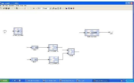
[image:5.595.152.454.64.336.2]From the Figure 5 above it is clear that the data is received at the VPSS (VPBE-RX) from the front-end. After the chunks of 16-bit words are received they are fed to the RS (7, 3) coder sub-system which is illustrated in Figure 6 below. From the Figure 6 we observe that there are two R-S (7, 3) coders working in parallel for the 16-bit word which is fed to this sub-system. This 16-bit word is broken up into two 8-bit words which are fed to each coder. Here to the 8 bit word a dummy bit is added to make it 9-bit word.
[image:5.595.54.557.381.665.2]Figure 3. The Model Based Design Methodology
Figure 4. The Transceiver Architecture
Matlab / Simulink
Real Time Workshop (DSP Model)
System Generator (FPGA Model)
Code Composer Studio Xilinx ISE Foundation
MBDK
BSDK
C Codes VHDL Codes
DSP executable file (.out) FPGA Configuration file (.bit)
Audio Codec
VPSS VPBE (TX)
VPSS VPFE (RX)
Audio Codec
DAC & ADC Control
RF Control
VPSS VPBE (RX)
VPSS VPFE (TX)
(7, 3) R-S
Coders P / S
QPSK Modulator
DAC A
DAC B IF RF Out
RF In IF
ADC
QPSK DeModulator
Matched Filter Detector
S / P (7, 3) R-S
DeCoders
Audio In Audio Out
16 bit samples
16 bit samples
16 bit samples
32 bit samples
16 bit samples
64 bit
samples 2 bit
samples
64 bit
samples 2 bit
samples
Front End DSP Model
This constitute the three 3-bit symbols for the R-S (7, 3) coder. The additional four symbols are calculated as described in section III above. To each of the seven symbols thus generated of three bits each, a dummy bit is added to make them 4-bit symbols. Hence, in all there are 7 dummy bits added and this comes out to be a code-word of 28-bits.
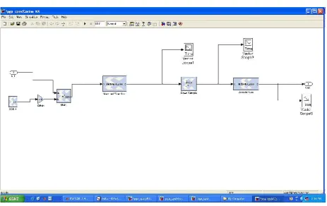
[image:6.595.71.529.147.419.2]To this another four dummy bits are added to make it a 32-bit word. This is performed for the two RS coders and adding together we get a 64-bit word. This is then passed through a parallel to serial converter which gives out chunks of 2-bit words. This is then fed to the Modulator sub-system. The Modulator sub-system is depicted in Figure 7 below.
Figure 5. The Back-End Model or the FPGA Model of the transceiver
[image:6.595.71.532.448.734.2]Here the bit input is fed to the MUX block which outputs either +1 or -1 for the 0o or180o phase shifts. This is then multiplied with the cosine or sine wave generated by the direct digital synthesizer, sample by sample, to give the effect of modulation. If the multiplication is with +1 then there is no change in phase of the sine (cosine) wave. If the multiplication is with -1 then there is the phase shift of 180o for that bit duration. The output from the sine (cosine) modulator is fed to two DACs respectively. After the DAC the output is fed to the IF section for frequency up-conversion and finally fed to the RF section for transmission.
[image:7.595.72.532.54.333.2]The signal transmitted is RF loop backed to the receiver antenna on the same platform where it is passed through the RF and IF blocks for frequency down-conversion. Then it is fed to the ADC for demodulation. The demodulator block is illustrated in Figure 8 above.The signal input to the ADC is fed to the sine (cosine) de-modulator after which it is fed to the sampled matched filter for sine (cosine) waves. The demodulator consists of the direct digital synthesized sine (cosine) signals of the same frequency as that generated in the modulators and a multiplier where the signal is multiplied with the direct digital synthesized sine (cosine) signals.
Figure 7.The Modulator Block for the In-phase (Quadrature) components
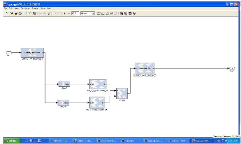
[image:7.595.68.532.351.643.2]This is then fed to the sampled matched filter which is matched to the sine (cosine) signals. The algorithm for the sampled matched filter is descried below in Section VI. The R-S decoders is illustrated in Figure 9 below. From the Figure 9 we observe that the 64-bit word input to this sub-system is broken up into two 32-bit word and given to the two R-S (7, 3) decoders. From this the most significant four dummy bits are stripped off. Again from each of the seven 4-bit words, the most significant bit is stripped off which forms 7-symbols of the R-S (7, 3) codes. The process of decoding is applied to this word and we get the 8-bit word at the output of each decoder. These two 8-bit words are concatenated into a single 16-bit word which is passed onto the VPSS (VPBE-TX) block. This is the interface between the FPGA and DSP models. The 16-bit word is received at the front-end where it is passed onto the CODEC for Digital to Analog conversion which is passed onto the speakers, which are connected to line-out jack of the data processing module of the model based development platform, for listening.
Sampled Matched Filter Detector
Since each of the basis functions ( ) ( )(sine & cosine respectively) is assumed to be zero outside the interval
0 ≤ ≤ . Here T is the bit duration. Consider, for example, a
linear filter with the impulse responseℎ ( ). With the received signal x(t) used as the filter input, the resulting filter output
( ) is defined by the convolution integral [11]:
( ) = ∫∞∞ ( )ℎ ( − ) ………(24)
Suppose, we now set the impulse response
ℎ ( ) = ( − ) ……..……(25)
That is the matched filter impulse response is a time reversed and delayed version of the basis function (sine or cosine). Then the resulting filter output is
( ) = ∫∞∞ ( ) ( − + ) ……….(26)
Sampling this output at time t = T, we get
( ) = ∫∞∞ ( ) ( ) ……….(27)
Since ( ) is zero outside the interval 0 ≤ ≤ , we finally get
( ) = ∫ ( ) ( ) ………..…(28)
Now this is the solution for the analog matched filter. Coming to the sampled matched filter, the basis functions can be written as ( ) ( ) respectively for sine and cosine signals generated by the direct digital synthesizers in the SDR baseband section. The optimal matched filter has the impulse response given as ℎ ( ). The resulting output, ( ) is defined by the convolution summation given as:
( ) = ∑∞ ( )ℎ ( − )
∞ ………(29)
For the matched filter matched to the basis functions, the impulse response of the matched filter is time reversed and delayed version of the input signal and assuming that the basis functions are zero outside the interval 1 ≤ ≤ , where N is the number of samples in one bit duration. Hence,
ℎ ( ) = ( − ) ………(30)
Hence, the Equation 29 can be re-written as
( ) = ∑ ( ) ( − + ) ………(31)
Sampling the filter output at n = N we get,
( ) = ∑ ( ) ( ) …………..….(32)
[image:8.595.59.547.55.347.2]Hence, the filter gives maximum output when sampled at n = N. Thus, the output SNR is greatly enhanced by the use of
matched filter. This operation is performed for both the In-phase and Quadrature components of the input signal taking the basis functions, cosine and sine, respectively.
SIMULATION RESULTS
[image:9.595.322.551.52.243.2]The simulation results of the transceiver taken at the back end model is illustrated in the Figures below.
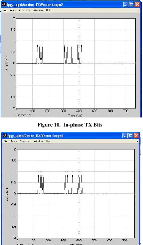
[image:9.595.46.286.156.565.2]Figure 10. In-phase TX Bits
Figure 11. In-phase RX Bits
Figure 12. Quadrature-phase TX Bits
Figure 13. Quadrature-phase RX Bits
From Figures 10 and 11 we observe that the transmitted and received bit stream perfectly match except for a small latency in the received bit stream. Similarly from Figures 12 and 13 we observe that the transmitted and received bit stream perfectly match except for a small latency in the received bit stream.
Real Time Results
Figure 14. Real Time RX waveform
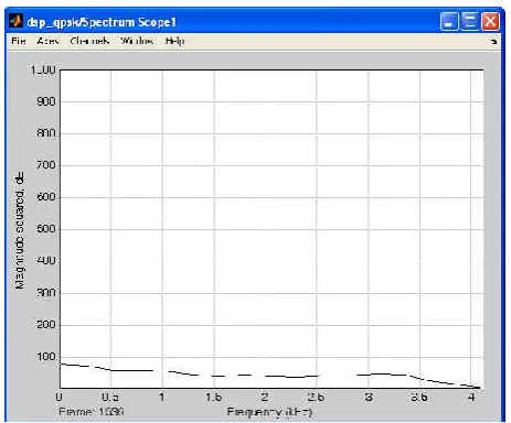
[image:9.595.314.556.368.565.2] [image:9.595.318.554.588.787.2]Figures 14 and 15 illustrates the real time received and transmitted waveform respectively. The transmitted and received waveform match except for some amplitude changes and certain latency. The frequency domain results is illustrated in the Figures 16 and 17 below.
Figure 16. Frequency Domain RX waveform
Figure 17. Frequency Domain TX waveform
From the Figures 16 and 17 it is clear that the frequency domain real time results for the TX and RX waveforms match each other.
Conclusion
The system described in this paper is realized successfully by using the channel coding in the form of R-S (7, 3) coding and decoding. The detection is performed by using sampled matched filter which greatly enhances the SNR at the output of the sampled matched filter. The results are taken for the simulation as well as the real time. The simulation result taken at the back-end of the transceiver perfectly match the transmitted bit stream as compared to the received bit stream. The real time result are taken both for time and frequency domain. The time domain results match except for some amplitude changes and some small latency. The frequency domain results match each other.
The advantage of the sampled matched filter is to enhance considerably the SNR at the output of the filter just before the threshold detector.
REFERENCES
Agarwal, A.; Boppana, L.; Kodali, R. K.; “Lagrange’s Polynomial based Farrow filterimplementation for SDR”, IEEE Region TEN Symposium, 2014, pp. 269-274.
Alluri, V.B., Heath, J.R.; Lhamon, M., “A New Multichannel, Coherent Amplitude Modulated, Time-Division Multiplexed, Software-Defined Radio Receiver Architecture, and Field-Programmabale-Gate-Array Technology Implementation”, IEEE Transactions on Signal Processing, VOL. 58, Issue: 10, 2010, pp. 5369-5384. Banani, S. A.; Vaughan, R. G., “Adaptive Reed-Solomon
Coding in Eigen-MIMO with Non-Adaptive Modulation”, 2011 IEEE Vehicular Technology Conference (VTC Fall), pp. 1-6.
Budroweit, J.; Koelpin, A.; “Design challenges of a highly integrated SDR platform formultiband spacecraft applications in radiation environments”, 2018 IEEE Topical Workshopon Internet of Space (TWIOS), 2018, pp. 9-12. Haykin, Simon, “Digital Communications”, John Wiley &
Sons, Inc., 1988, ISBN 0-471-62947-2.
Mohamed, K.E.; Ali, B.M.; Jamuar, S.S.; Khatun, S.; Ismail, A., “Implementation of CDMA Transmitter for a multi-standard SDR base band platform”, Asia-Pacific Conference on Communications, 2007, APCC 2007, pp. 303-306.
Mohamed, K.E.; Ali, B.M.; Jamuar, S.S.; Khatun, S.; Ismail, A., “Design of Multi-standard protocol for SDR base band transceiver”, IEEE International Conference on Telecommunications and Malaysia International Confwerence on Communications, 2007. ICT-MICC 2007. pp. 577 - 581.
Noseworthy, Joshua; Kulp, James, “Standard Interfaces for FPGA Components”, IEEE Military Communications Conference, 2007, MILCOM 2007, pp. 1-5.
Politis, C.; Maleki, S.; Duncan, J. M.; Krivochiza, J.; Chatzinotas, S.; Ottesten, B.; “SDRImplementation of a Testbed for Real-Time Interference Detection With SignalCancellation”, IEEE Access, 2018, pp. 20807 – 20821.
Qiwei Zhang; Kokkeler, A.B.J.; Smit, G.J.M., “A System-level Design Method for Cognitive Radio on Reconfigurable Multi-processor Architecture”, IEEE International Symposium on System-On-Chip, 2007, pp. 1-4.
Rodriguez-Pareram, S.; Bourdoux, A.; Horlin, F.; Carrabina, J.; Van der Perre, L., “Front-End ADC Requirements for Uniform Bandpass Sampling in SDR”, IEEE 65th Vehicular Technology Conference, 2007. VTC2007-Spring. Pp. 2170 – 2174.
Schuster, T.; Bruna, D.N.; Bougard, B.; Derudder, V.; Hoffmann, A.; Van der Perre, L., “Subword-Parallel VLIW Architecture Exploration for Multimode Software Defined Radio”, IEEE Workshop on Signal Processing Systems Design and Implementation, SIPS’06, 2006, pp. 351 – 356. Sklar, Bernard; Ray, Pabitra K,“Digital Communications”,
Pearson Publications, SecondEdition, 2013, ISBN 978-81-317-2092-9.
Zlydareva, O.; Sacchi, C.; “Multi-Standard WIMAX/UMTS System Framework Based on SDR”, Aerospace Conference, 2008 IEEE, pp. 1-13.