Cite as: Rev. Sci. Instrum. 90, 094701 (2019); https://doi.org/10.1063/1.5083797
Submitted: 30 November 2018 . Accepted: 19 August 2019 . Published Online: 10 September 2019
G. A. Stimpson , M. S. Skilbeck, R. L. Patel, B. L. Green , and G. W. Morley
ARTICLES YOU MAY BE INTERESTED IN
Surface condensation sensor board for damp heat chamber
Review of Scientific Instruments
90
, 095102 (2019); https://doi.org/10.1063/1.5100745
The digital mirror Langmuir probe: Field programmable gate array implementation of
real-time Langmuir probe biasing
Review of Scientific Instruments
90
, 083504 (2019); https://doi.org/10.1063/1.5109834
An open-source high-frequency lock-in amplifier
Cite as: Rev. Sci. Instrum.90, 094701 (2019);doi: 10.1063/1.5083797
Submitted: 30 November 2018•Accepted: 19 August 2019•
Published Online: 10 September 2019
G. A. Stimpson,1,2,a) M. S. Skilbeck,1 R. L. Patel,1,2 B. L. Green,1 and G. W. Morley1,2,b)
AFFILIATIONS
1Department of Physics, University of Warwick, Coventry CV4 7AL, United Kingdom
2Diamond Science and Technology Centre for Doctoral Training, University of Warwick, Gibbet Hill Road, Coventry CV4 7AL, United Kingdom
a)Email:[email protected] b)Email:[email protected]
ABSTRACT
We present characterization of a lock-in amplifier based on a field programmable gate array capable of demodulation at up to 50 MHz. The system exhibits 90 nV/√Hz of input noise at an optimum demodulation frequency of 500 kHz. The passband has a full-width half-maximum of 2.6 kHz for modulation frequencies above 100 kHz. Our code is open source and operates on a commercially available platform.
© 2019 Author(s). All article content, except where otherwise noted, is licensed under a Creative Commons Attribution (CC BY) license (http://creativecommons.org/licenses/by/4.0/).https://doi.org/10.1063/1.5083797., s
I. INTRODUCTION
The lock-in amplifier (LIA) is an invaluable tool in scientific instrumentation1allowing the extraction of weak signals from noisy backgrounds, even where the amplitude of the noise is much greater than the signal.2First described in 1941, early LIAs were based on heaters, thermocouples, and transformers.3More modern LIAs have been fully digital4–7 or implemented on field programmable gate array (FPGA) devices,8–14which are able to exceed the performance of their analog counterparts.15 However, the cost of modern LIAs may prove prohibitive, particularly in cases where large numbers of input channels are required. By employing Red Pitaya hardware, we are able to define an open-source LIA solution that is comparable with considerably more costly approaches.
Characterized by a wide dynamic range and the ability to extract signal from noisy environments,16LIAs are phase sensitive detectors17due to their operating principles. A reference signal in the form of a sinusoidal wave is generated either internally by the LIA itself, along with a cosinusoidal wave, or externally by some other sources that can also be manipulated to form a cosinusoidal reference. This reference is multiplied by the input signal18that car-ries the desired data modulated at the reference frequency.19A low pass filter is then used before outputting the signal. In this way, the LIA amplifies and outputs the component of the input signal that is at the reference frequency, attenuating noise at other frequen-cies.20 Components out of phase with the sine reference will also
be attenuated due to orthogonality of the sine and cosine functions of equal frequency,21and hence, the LIA is considered phase sensi-tive.22Components in phase with the sine function will result in a nonzero value in the X output, while those in phase with the cosine function will produce a nonzero value in the Y output. X and Y can be combined byR=
√
X2+Y2to provide a magnitude value,23while
phaseϕ=arctanYX.
FPGAs offer easily implementable microcircuitry design via the use of hardware description language (HDL) such as Verilog or VHDL. A broad range of applications can be realized using these devices,24including LIAs without recourse to detailed knowledge of microelectronics.25
The Red Pitaya STEMlab 125-14 is a single board computer (SBC) with an integrated FPGA in the form of a Xilinx Zynq 7010 SoC,26 allowing for the implementation of reprogrammable microarchitecture that would otherwise necessitate dedicated hard-ware. The reprogrammability27 of this FPGA makes it applicable for the LIA functionality described here and allows for further expansion and modification by end users. Two DC coupled analog inputs are available in the form of user selectable±1 V or±20 V,
125 MS/s analog-to-digital converters (ADCs—Linear Technolo-gies LTC2145CUP-1428) with an input impedance/capacitance of 1 MΩ/10 pF.
We demonstrate that this device shares many capabilities with more expensive alternatives such as a sweepable internal signal genera-tor, single or dual input/output modes, wave form control, and the ability to increase the number of available inputs and outputs by interfacing across multiple STEMlab units.
Comparison is made with the Zurich Instruments HF2LI LIA, which is specified for operation up to 50 MHz demodulation fre-quency.30While an extensive software application is provided with
the HF2LI, the open source nature and readily available software and hardware of the LIA presented here allow for an attractive option where cost is a consideration. Research into low-cost FPGA based LIAs has produced a number of alternatives,25including high
res-olution designs operating at up to 6 MHz demodulation,31,32and simulations have been presented for a high frequency LIA based on the Red Pitaya STEMlab.33Typically, FPGA LIAs have been devel-oped with specific experimental objectives.13,14,34 The STEMlab is
the basis for a range of related measurement instrumentation from PyRPL, including an LIA.35–37A low cost FPGA-based LIA has also been developed which operates at a low demodulation frequency,38 and FPGA-based LIAs have been compared with analog devices in terms of signal accuracy.39However, we believe that this article is the first to characterize a high frequency, open source LIA. The open source code may lead to a range of future uses in research, education, and industry.
II. METHODS
A. Hardware and software
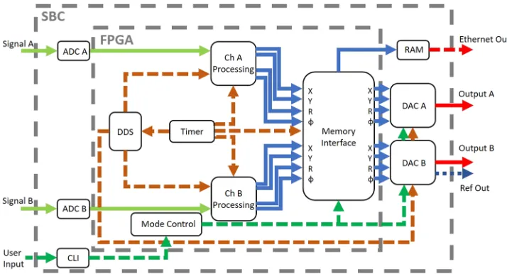
The FPGA system design and implementation was performed using software provided by the manufacturer of the FPGA, Xilinx. A simplified version of the design circuitry block diagram can be seen
inFig. 1. Signals received by the ADCs are passed to the processing blocks where they are multiplied by the reference signal [which is generated internally by direct digital synthesis (DDS)] and filtered using a single pole infinite impulse response (IIR) filter. The result-ing output is written to the SBC’s random access memory (RAM) via the FPGA’s memory interface block. This data is then written to a ramdisk file also contained within the STEMlab’s RAM, alleviat-ing high read/write workloads which were observed to cause critical failures of the SD card. The data are also passed to the on-board digital-to-analog converters (DACs) along with the reference signal that is used to modulate the desired signal. This reference can be extracted via the DAC output for external use.
Data retrieval from the STEMlab to a host computer can be achieved via the DACs that are provided with SubMiniature version A (SMA) connections for output to an oscilloscope. These DACs have 14-bit resolution combined with 125 MS/s data rate. Non-offset, digital amplification of up to 2000 times the raw output is available. However, noise introduced by the DACs makes the out-put undesirable in cases where small changes in signal intensity are to be detected. Alternatively, data may be transferred to a host per-sonal computer (PC) via file transfer from the STEMlab’s RAM. This produces low noise data but can only be performed on the entirety of the LIA’s allocated storage space of approximately 65 megabytes (MB). While this process may last for tens of seconds, all data (X, Y, R, andϕ) for both output channels are received simultane-ously. Further limitations include the inability to operate using an external lock-in reference, cross talk that can occur between the two input channels and no facility for subtraction of channels (e.g., A-B). Due to the programmable nature of the STEMlab, end users are able to implement their own data transfer methods, which may be shown to alleviate some or all of these limitations.
[image:3.594.116.473.429.622.2]While the FPGA is responsible for signal processing and data transfer, parameter setting takes place on the STEMlab’s Linux SBC. This device is packaged along with the FPGA on the STEMlab board, allowing the user to operate the Red Pitaya LIA (RePLIA) or any other custom FPGA application entirely using the STEMlab itself. Parameter setting and system control are performed using C and Python codes written specifically for use with the LIA. These codes may be accessed via secure shell (SSH) or a terminal emulator but, in practice, are accessed via a Java-based graphical user interface (GUI) on a client computer that allows the user to largely ignore the STEM-lab’s Linux element. This open-source GUI allows for the setting of all available RePLIA parameters.
B. Characterization methodology
Data were extracted from both LIAs via Ethernet connection. In the case of the RePLIA aboard the STEMlab, this avoided noise from its DACs which were found to increase noise by up to three orders of magnitude.
Noise for both LIAs during operation was measured at various demodulation frequencies with no input signal present and with a constant amplitude signal produced with an Agilent N5172B EXG vector signal generator. Similarly, noise was measured while varying the time constant of the LIAs with the demodulation frequency fixed at the value determined to be the least noisy by the previous method. As with the input noise, these data are presented after a fast Fourier transform (FFT).
Passbands for each LIA at various demodulation frequencies were obtained by applying a constant amplitude signal at the spec-ified demodulation frequency. This signal was then combined with a sweep between the minimum and maximum frequencies passing through the demodulation frequency, with a sweep time of 10 s.
1. Zurich instruments HF2LI
The HF2LI provides a built in input noise measurement pro-tocol. The experimental conditions detailed in the HF2LI user notes were replicated,30and the input noise was measured. Noise was col-lected while the inputs were terminated for periods of 1, 10, and 100 s. This noise was then subjected to a FFT, and the noise level was assessed and compared with the manufacturer’s stated input noise level of 5 nV/√Hz at 1 MHz demodulation for the output frequencies greater than 10 kHz.40
2. Red Pitaya lock-in amplifier
Optimal operational parameters were deduced by examining the output of the RePLIA at varying demodulation frequencies and time constants. The optima chosen were those which resulted in the lowest output noise level. This behavior was examined both with an applied signal and with the terminated inputs. The RePLIA maintains capability over a wide range of demodulation frequen-cies (10 kHz–50 MHz), which were also characterized, but figures are quoted with respect to optimal parameters unless otherwise stated.
III. RESULTS
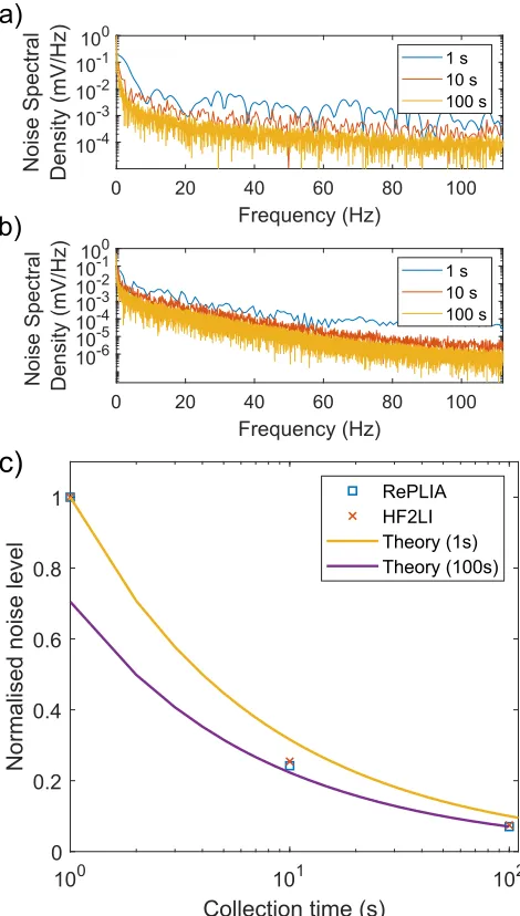
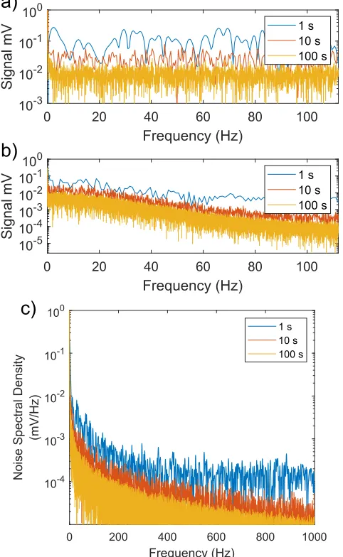
Figure 2shows input noise spectral density for both LIAs at 1 s, 10 s, and 100 s collection periods. Increasing collection timetwas
FIG. 2. Noise spectral density from (a) RePLIA at 500 kHz demodulation with a 1 ms time constant (with 1 s data zero padded) and (b) HF2LI at 1 MHz demodula-tion and 700μs time constant at 1 s, 10 s, and 100 s collection times (output data are R for both channels). (c) Noise level decays with an increased collection time close to the predicted√trelationship (top trace) calculated based on the noise measured after 1 s of collection. The lower trace indicates theoretical values back calculated from the 100 s data point.
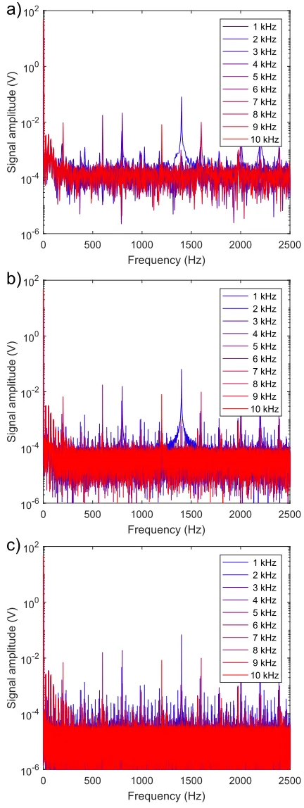
[image:4.594.310.545.86.500.2]FIG. 3. FFTs of terminated input data, extracted via file transfer, at various RePLIA demodulation frequencies with 100 s collection time. Two distinct noise regimes seem to exist, with demodulation frequencies above 100 kHz producing signifi-cantly lower noise. Time constants were varied depending on the demodulation frequency (seeAppendixes AandB). Note that low frequency and high intensity data have been cropped for visual clarity.
sensitivities of 89, 66, and 60 nV/ √
Hz. When the RePLIA was oper-ated using the conditions stipuloper-ated for measurement of the HF2LI input noise, the noise levels are 131, 133, and 130 nV/
√
Hz. This shows that the optimal operating parameters for the HF2LI differ
from those appropriate to the RePLIA. It should be noted that the manufacturer specified sampling rate for the HF2LI limits the span of the FFT output to 120 Hz. Frequencies beyond this limit can be found in the HF2LI’s user manual in section 8.4 on page 665.30
A wider output frequency plot for the RePLIA can be found in
Appendixes AandB(Fig. 13).
The noise spectrum for the HF2LI [Fig. 2(b)] shows greater noise below 80 Hz and lower noise at higher output frequencies. By contrast, the RePLIA shows a higher level of noise that is largely steady up to 120 Hz [Fig. 2(a)] output frequency.
Figure 3shows FFTs of the RePLIA output collected for 100 s at a range of demodulation frequencies, with time constants optimized for the relevant demodulation period (seeAppendixes A andB). There is a marked difference in noise at demodulation frequencies below 100 kHz, although above this threshold the noise is roughly constant.
Output from the RePLIA digital-to-analog converters (DACs) was also produced (see Appendixes A and B), showing a con-stant noise level at frequencies below 100 kHz. Although this noise level is several orders of magnitude greater than that incurred in data extracted via the Ethernet connection, this may be an acceptable trade-off in certain cases. This consistency suggests that noise inherent to the DACs is the limiting factor when obtain-ing data usobtain-ing this method, although this noise can be reduced as described in Ref.28. Signal-to-noise as measured at the DACs increases with an increase in the DAC multipliers, plateauing toward saturation of the RePLIA’s outputs (see Fig. 7in Appendixes A
andB).
[image:5.594.47.287.87.239.2] [image:5.594.39.550.400.704.2]FIG. 5. Demodulated RePLIA output against the input voltage, operating at 500 kHz demodulation for a±1 V input range. Solid red line is a linear fit of the
0–0.7 V linear region.
Figures 4(a)and4(b)show the shape of LIA passbands when modulating at varying frequencies with time constants optimized for each frequency. The HF2LI demonstrates a narrower band with less transmission at unwanted frequencies. These pass-bands are shown to be approximately Lorentzian in line shape with a full-width half-maxima of 2.6 kHz for demodulation frequen-cies above 100 kHz (seeAppendixes AandB), and they begin to reduce in intensity above 30 MHz demodulation with the HF2LI, whereas the output is consistent up to 50 MHz demodulation with the RePLIA. Figure 5(c) shows the normalized output at mega-hertz demodulation frequencies for both LIAs. The half power point is indicated (V√max
2, whereVmaxis the peak voltage output),
which for the RePLIA is encountered at a demodulation frequency of around 60 MHz, which is close to half of the device’s 125 MHz sample rate, as can be expected from the Nyquist sampling theorem.41
Linearity of the output relative to the input is demon-strated in Fig. 5. Input voltages were varied, and the resul-tant DAC output voltage were measured for both the ±1 V
and ±20 V input ranges. Linearity is observed over ±700 mV
and ±1100 mV, respectively. Outside these regions, the
STEM-lab’s input, having only 14 bits, introduces significant nonlinear-ities, as does the improper impedance matching of the RePLIA’s inputs.
IV. CONCLUSIONS
The RePLIA performs lock-in amplification at frequencies up to 50 MHz, with an input noise level of 90 nV/√Hz. The respective figures from the Zurich Instruments HF2LI (50 MHz demodulation with 5 nV/√Hz input noise) show that the FPGA LIA detailed in this article is an open source alternative.
ACKNOWLEDGMENTS
We thank Ben Breeze and Matt Dale for assistance and advice. This research was funded by Bruker Biospin and the Engineer-ing and Physical Sciences Research Council (EPSRC) via Grant No. EP/L015315/1, and G. W. Morley was supported by the Royal Society.
APPENDIX A: OPERATIONAL NOTES
The RePLIA was operated in a dual channel input mode with the output producing amplitude data. These data were collected at a rate of 20 ksamples/s. It is important to note that in setting a sample rate, the actual rate per sample will be 1/8of that set, as
[image:6.594.58.280.84.283.2] [image:6.594.305.552.337.479.2]the set rate includes one sample per output channel per time incre-ment (2 input channels comprising R, X, Y, andϕfor each input channel). This sample rate is dependent on both the system being measured and the hardware over which data are transmitted but can be set by the user to any rate within the sample rate range of
TABLE I. Experimental parameters used for the measurement of HF2LI input noise, as detailed in manufacturer’s instructions.
HF2LI input noise settings
Setting Parameter Value
Signal input
Range 10 mV AC On Diff Off 50 Ω On Demodulator low-pass filter Bandwidth 3 dB 100 Hz
Order 4 Oscillator Frequency 1 MHz Signal output Switch Off
TABLE II. Time constantsτfor RePLIA at various demodulation frequencies. The central column contains the minimum usable time constant and the right-hand column details the actual time constants used which were determined by ensuring a near-Lorentzian passband at the relevant demodulation frequency. Note that this table is not exhaustive and longer/shorter time constants may be used.
Time constants (τ)
Fmod(MHz) τmin(ms) τ(ms)
0.001 10 100
0.01 1 100
0.1 0.1 10
0.5 2×10⁻² 1
1 1×10⁻² 1
10 1×10⁻³ 1
[image:6.594.306.553.563.689.2]the STEMlab, although this sample rate may ultimately affect the accuracy of resultant signals. When obtaining data via the DAC out-puts, collection has been performed by a Pico Technology Picoscope 4424 digital oscilloscope. The Picoscope and DAC outputs were also used when determining the time constants for the RePLIA. Data extracted via the RePLIA’s Ethernet port were converted to milli-volt values by dividing the actual numerical value by 2.1×10⁶, a
conversion factor that was determined by comparing the Ethernet values with the corresponding values produced at the DACs with no DAC multiplication applied.
The Zurich Instruments HF2LI was operated according to the instructions laid out in section 3.5 of the HF2 User Manual,30using
the parameters inTable I.
FIG. 6. (a) FFT of 10 kHz demodulation data taken from the RePLIA’s DAC outputs, demonstrating significantly greater noise than the data taken from the Ethernet output. (b) Output signal to noise ratio from the DAC outputs improves dramati-cally with demodulation frequency throughout lower frequency ranges due to the increased signal.
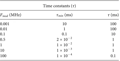
[image:7.594.319.539.84.633.2] [image:7.594.47.293.245.636.2]The time constants detailed inTable IIwere used for measure-ments made with the RePLIA. For frequencies in between those listed, the time constant corresponding to the lower frequency was used. Minimum time constantsτminhave been determined by τmin = 10/fmod, where fmod is the demodulation frequency. This
ensures that for a given time constant, 10 modulation periods or more elapse during the time constant. The actual time constants used were chosen based on the line shape of passbands as seen in
Fig. 5(a)in the main text. Time constants were made as large as possible without distortion of the Lorentzian line shape of these passbands.
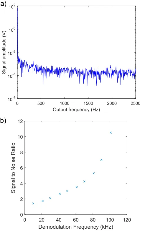
Figure 6(a)shows an FFT of the terminated input data at 10 kHz. These data were extracted from the digital-to-analog convert-ers (DACs), with the noise level indicating that the DACs themselves are the most significant source of noise. Contrasting this withFig. 3, where we see that without DAC noise, the varying demodulation fre-quency causes a distinct change to noise levels.Figure 7(b) demon-strates an increase in the output signal to noise ratio with increasing demodulation frequency.
Figure 7(a) shows the effect on an FFT while varying the DAC amplification multiplier, with the extremes in this range shown inFig. 7(b). There is no significant difference in noise level between these extremes. AlthoughFig. 7(c)shows that an increase in the DAC multiplier does improve the signal-to-noise ratio, care should be taken not to saturate the STEMlab’s 1 V maximum output.
Figure 8demonstrates the effect of the time constant on the shape of the passband for a given demodulation frequency, with 500 kHz used as an example. Excessively long time constants produce a narrower passband at the expense of line shape; fringes
FIG. 8. The effect of the time constant setting on the resulting passband. An 80 kHz sweep over 10 s through the demodulation frequency of 500 kHz at varying time constants results in distortion of the passband. Longer time constants result in fringes in the unwanted frequency regions, and shorter time constants result in excessive acceptance of unwanted frequencies. For 500 kHz, a time constant of 1 ms was chosen as a suitable compromise. The small section of the sweep output shown above shows only the part of the passband affected by the time constant.
[image:8.594.319.535.84.658.2] [image:8.594.64.276.427.611.2]appear at output frequencies close to but greater than the demod-ulation frequency, leading to the distortion of output signals. Shorter time constants produce a more consistent line shape at the cost of passband linewidth. Further to this, extremely short time constants (below those detailed in Table II) are unable to detect changes on time scales appropriate to the demodulation frequency. In terms of software, the time constant can be set to any value above 9 × 10⁻⁶ s. However, appropriate setting of
the time constant is necessary to ensure the correct represen-tation of output signals, and an understanding of the physical nature of systems being measured is also necessary for accurate results.
Figure 9 shows FFTs of low demodulation frequency data at varying collection times. Certain frequency elements are evident throughout, which are not evident at higher demodula-tion frequencies. These components are visible in data extracted both via the DACs and via the STEMlab’s Ethernet port.
Figure 10shows the effect of time constant on noise. Although noise decreases with longer time constants, signal distortions as seen inFig. 8limit the choice of time constant used.
Figure 11 shows the measured 10 MHz passband of both the RePLIA and HF2LI along with a Lorentzian fit of the data, demonstrating a rough conformation with such a line shape. These data give a full-width half-maximum of 2.6 kHz for the RePLIA and 2 kHz for the HF2LI. Figures 8 and 9 both contain arti-facts arising from the single order filter. Increasing the order of the filter may reduce the prominence of these features, although experiments with the HF2LI suggest that such benefits may be marginal.
[image:9.594.321.535.85.419.2]Higher noise at lower frequencies, as seen inFig. 3, is consistent with flicker noise of the input stage, as demonstrated inFig. 12, in that it is of the form of 1/f.
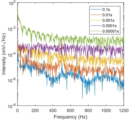
[image:9.594.57.277.454.658.2]FIG. 10. FFTs of noise at varying time constant at a demodulation frequency of 500 kHz. Note that the 0.00 001 s trace is below the minimum time constant as detailed inTable II.
FIG. 11. (a) RePLIA and (b) HF2LI 10 MHz passbands with Lorentzian fits with 2.6 kHz and 2 kHz linewidths, respectively. Note that the x-axes cover different ranges for these data.
FIG. 12. FFT of the signal demodulated at 30 kHz, with a fit off(x) =a+b⋅1/f,
[image:9.594.316.546.467.664.2]APPENDIX B: HARDWARE AND SOFTWARE NOTES
Largely, the RePLIA is limited by the factors introduced by the STEMlab’s hardware and software. The maximum sample rate of the demodulated signal corresponds to the output sample rate of the STEMlab (125 MS/s) when using the DAC outputs. However, this sampling rate is limited instead by the network connection when extracting data via the Ethernet adapter.
Mathematical operations such asAout=Ain−Binhave not been
implemented at the current time, although this is entirely plausible by adding such functionality within the FPGA code.
Power consumption for the RePLIA is 4 W when idle and<6 W
[image:10.594.47.288.231.623.2]during lock-in operation.
FIG. 13. FFTs of noise data from (a) RePLIA at 500 kHz demodulation with a 1 ms time constant (with 1 s data zero padded) and (b) HF2LI at 1 MHz demodulation and 700μs time constant, at 1 s (blue), 10 s (red), and 100 s (yellow) collection time (output data is R for both channels). (c) Noise spectral density of the RePLIA at the above input parameters with a wider output frequency spectrum than in Fig. 2.
Cross talk between input channels results in a signal 0.3% of the input signal amplitude reflected in the secondary input. The output voltage range is limited by the board to±1 V.
Figure 13 represents the same data as Fig. 2 in the main text, but as plain FFTs of noise data as opposed to noise spectral density.
The RePLIA has been used for magnetometry using an ensem-ble of nitrogen vacancy centers in diamond. We intend to apply this technique to magnetocardiography, where it would be preferable to use approximately 200 sensors, requiring 100 dual channel lock-in amplifiers.42
REFERENCES
1
J. Leis, P. Martin, and D. Buttsworth, “Simplified digital lock-in amplifier algorithm,”Electron. Lett.48, 259–261 (2012).
2L. C. Caplan and R. Stern, “An inexpensive lock-in amplifier,”Rev. Sci. Instrum.
42, 689–695 (1971). 3
W. C. Michels and N. L. Curtis, “A pentode lock-in amplifier of high frequency selectivity,”Rev. Sci. Instrum.12, 444 (1941).
4X. Wang, “Sensitive digital lock-in amplifier using a personal computer,”Rev.
Sci. Instrum.61, 1999–2001 (1990). 5
P.-A. Probst and A. Jaquier, “Multiple-channel digital lock-in amplifier with ppm resolution,”Rev. Sci. Instrum.65, 747 (1998).
6M. Hofmann, R. Bierl, and T. Rueck, “Implementation of a dual-phase
lock-in amplifier on a TMS320C5515 digital signal processor,” lock-in5th European DSP Education and Research Conference (EDERC)(IEEE, 2012), pp. 20–24.
7M. Osvaldo Sonnaillon and F. J. Bonetto, “A low-cost, high-performance, digital
signal processor-based lock-in amplifier capable of measuring multiple frequency sweeps simultaneously,”Rev. Sci. Instrum.76, 024703 (2005).
8G. Macias-Bobadilla, J. Rodríguez-Reséndiz, G. Mota-Valtierra, G.
Soto-Zarazúa, M. Méndez-Loyola, and M. Garduno-Aparicio, “Dual-phase lock-in amplifier based on FPGA for low-frequencies experiments,” Sensors 16, 379 (2016).
9
G. C. Giaconia, G. Greco, L. Mistretta, and R. Rizzo, “Exploring FPGA-based lock-in techniques for brain monitoring applications,”Electronics6(1), 18 (2017).
10
S. G. Castillo and K. B. Ozanyan, “Field-programmable data acquisition and processing channel for optical tomography systems,”Rev. Sci. Instrum.76, 095109 (2005).
11
A. Moreno-Baez, G. Miramontes-de Leon, C. Sifuentes-Gallardo, E. Garcia-Dominguez, D. Alaniz-Lumbreras, and J. A. Huerta-Ruelas, “FPGA implemen-tation of a 16-channel lock-in laser light scattering system,” inIEEE Electronics, Robotics and Automotive Mechanics Conference(IEEE, 2010), pp. 721–725. 12A. Patil and R. Saini, “Design and implementation of FPGA based linear
all digital phase-locked loop,” inInternational Conference on Green Computing Communication and Electrical Engineering (ICGCCEE)(IEEE, 2014), p. 1. 13D. Divakar, K. Mahesh, M. M. Varma, and P. Sen, “FPGA-based lock-in
amplifier for measuring the electrical properties of individual cell,” inIEEE 13th Annual International Conference on Nano/Micro Engineered and Molecular Systems (NEMS)(IEEE, 2018), pp. 1–5.
14
A. Chighine, E. Fisher, D. Wilson, M. Lengden, W. Johnstone, and H. McCann, “An FPGA-based lock-in detection system to enable chemical species tomogra-phy using TDLAS,” inIEEE International Conference on Imaging Systems and Techniques (IST)(IEEE, 2015), pp. 1–5.
15M. Carminati, G. Gervasoni, M. Sampietro, and G. Ferrari, “Note: Differential
configurations for the mitigation of slow fluctuations limiting the resolution of digital lock-in amplifiers,”Rev. Sci. Instrum.87(2), 026102 (2016).
16M. Meade,Lock-in Amplifiers: Principles and Applications(Peter Peregrinus
Ltd., 1983). 17
18
J. H. Scofield, “Frequency-domain description of a lock-in amplifier,”Am. J. Phys.62(2), 129–133 (1994).
19P. Horowitz and W. Hill,The Art of Electronics, 2nd ed. (Cambridge University
Press, 1989). 20
E. Theocharous, “Absolute linearity characterization of lock-in amplifiers,”
Appl. Opt.47(8), 1090–1096 (2008).
21S. DeVore, A. Gauthier, J. Levy, and C. Singh, “Development and evaluation of
a tutorial to improve students’ understanding of a lock-in amplifier,”Phys. Rev. Phys. Educ. Res.12(2), 020127 (2016).
22See https://www.thinksrs.com/downloads/pdfs/applicationnotes/AboutLIAs.
pdffor Stanford Research Systems: About Lock-in Amplifiers. 23
See https://www.zhinst.com/sites/default/files/li_primer/zi_whitepaper_ principles_of_lock-in_detection.pdffor White paper: Principles of lock-in detec-tion and the state of the art; accessed August 19, 2019.
24
T. Qian, L. Chen, X. Li, H. Sun, and J. Ni, “A 1.25 Gbps programmable FPGA I/O buffer with multi-standard support,” inIEEE 3rd International Conference on Integrated Circuits and Microsystems (ICICM)(IEEE, 2018), pp. 362–365. 25
R. Li and H. Dong, “Design of digital lock-in amplifier based on DSP builder,” inIEEE 4th Information Technology and Mechatronics Engineering Conference (ITOEC)(IEEE, 2018), pp. 222–227.
26
Seehttps://www.redpitaya.com/f130/STEMlab-boardfor Red Pitaya STEMlab Board; accessed September 5, 2018.
27A. Restelli, R. Abbiati, and A. Geraci, “Digital field programmable gate
array-based lock-in amplifier for high-performance photon counting applications,”Rev. Sci. Instrum.76(9), 093112 (2005).
28See https://www.analog.com/media/en/technical-documentation/data-sheets/
21454314fa.pdffor LTC2145CUP-14; accessed August 19, 2019. 29
Seehttps://github.com/WarwickEPR/RePLIAfor Warwick EPR Group GitHub Repository; accessed August 19, 2019.
30Seehttps://www.zhinst.com/manuals/hf2for Zurich Instruments. HF2 User
Manual - LabOne Edition; accessed 2018.
31
G. Gervasoni, M. Carminati, G. Ferrari, M. Sampietro, E. Albisetti, D. Petti, P. Sharma, and R. Bertacco, “A 12-channel dual-lock-in platform for magneto-resistive DNA detection with PPM resolution,” inIEEE Biomedical Circuits and Systems Conference (BioCAS) Proceedings(IEEE, 2014), pp. 316–319.
32G. Gervasoni, M. Carminati, and G. Ferrari, “A general purpose
lock-in amplifier enabllock-ing sub-PPM resolution,” Procedia Eng. 168, 1651–1654 (2016).
33L. H. Arnaldi, “Implementation of an AXI-compliant lock-in amplifier on the
red pitaya open source instrument,” inIEEE Eight Argentine Symposium and Conference on Embedded Systems (CASE)(IEEE, 2017), pp. 1–6.
34Y. Sukekawa, T. Mujiono, and T. Nakamoto, “Two-dimensional digital lock-in
circuit for fluorescent imaging of odor biosensor system,” inNew Generation of CAS (NGCAS)(IEEE, 2017), pp. 241–244.
35See https://pyrpl.readthedocs.io/en/latest/gui.html for PyRPL GUI Manual;
accessed August 19, 2019. 36
See https://ln1985blog.wordpress.com/2016/02/07/adding-voltage-regulators-for-the-redpitaya-output/-stage/for Adding voltage regulators for the RedPitaya output stage; accessed August 19, 2019.
37
Seehttps://ln1985blog.wordpress.com/2016/02/07/red-pitaya-dac-performance/
for Red Pitaya DAC performance; accessed August 19, 2019.
38Seehttps://delacor.com/products/lock-in-amplifier/for Lock-in amplifier for
myrio; accessed August 19, 2019. 39
J. Vandenbussche, P. Lee, and J. Peuteman, “On the accuracy of digital phase sensitive detectors implemented in FPGA technology,”IEEE Trans. Instrum. Meas.63(8), 1926–1936 (2014).
40
Seehttps://www.zhinst.com/sites/default/files/zi_hf2li_leaflet_web_0.pdffor ZI HF2LI Leaflet; accessed October 02, 2018.
41C. E. Shannon, “Communication in the presence of noise,”Proc. IRE
37, 10–21 (1949).
42