Abstract— IGBT modules which can fail to stable short circuit mode have major applications in electricity network related fields. Sn-3.5Ag solder joints and sintered Ag joints for the die attachment and Mo, Cu, Sn-3.5Ag, Al and Ag foils for the top side insert material in press pack like single IGBT samples have been investigated using overcurrent and current passage tests. The results reveal that Sn-3.5Ag solder joints in combination with Sn-3.5Ag, Al or Ag foils can be employed to achieve stable short circuit failure mode, where the best results are achieved with Ag foils. This can be attributed to the formation of conductive networks/channels through the failed IGBT, and good alignment between the residual top side insert material and the failed IGBT.
Index Terms—Electronics packaging, failure to short circuit, finite element analysis, overcurrent failure, power module, scanning electronic microscopy, semiconductor device packaging.
I. INTRODUCTION
NSULATED gate bipolar transistor (IGBT) modules which can achieve stable short circuit failure mode (SCFM) in the event of device destruction are important in electricity network related fields. In particular, they have intrinsic importance in systems which are installed remotely, or at places which are not easy to access or where the cost of unscheduled maintenance is prohibitively high [1]. This is because in series connected strings of IGBT modules where a level of redundancy can be employed, the strings can still function correctly in the event of failure occurring in one or several redundant modules, where failures can then be replaced in the next scheduled maintenance cycle.
There are two commercially available IGBT modules which have been reported to have the ability to achieve SCFM. The first one; Press-Pack IGBT module (PPIM) by Westcode [2,3] and the second; StakPak IGBT module (SPIM) by ABB [4,5]. Both IGBT modules require very flat and dimensionally accurate components, and their manufacturing process is
This paper was partly presented at PCIM Asia 2016 Conference, 28-30 June, 2016, Shanghai, China. This work was supported by the Innovative Electronics Manufacturing Research Centre (IeMRC) funded by the UK Engineering and Physical Sciences Research Council (EPSRC) through research grant EP/H03014X/1.
J. F. Li, M. Corfield and C. M. Johnson are with the Department of Electrical and Electronic Engineering, The University of Nottingham, University Park, Nottingham NG7 2RD, UK (e-mail: Jianfeng.Li@ nottingham.ac.uk, [email protected], Mark.Johnson@ nottingham.ac.uk).
I. Yaqub is with Dynex Semiconductor Limited, Doddington Road, Lincoln LN6 3LF, UK (email: [email protected]).
therefore complicated and expensive. To overcome this problem, a semiconductor power module with bonded metallic layers and/or base plates on both sides of the power devices was further proposed and patented by ABB [6].
In the early PPIM by Westcode [2,7-9], Mo shims were applied on both sides of the Si IGBT or other power devices by pressure contact. In later PPIMs by ABB [5,10,11], Al or Ag platelet was placed on the top side of each IGBT with individual spring press pins, and the IGBTs were bonded on the substrate/base plate with Pb-Sn-based solder joint. In later PPIMs patented by ABB [6], Al, Ag, Au, Cu and their alloys with a thickness at least 50% of the Si IGBT or other power devices were recommended for sinter on the top sides of the power devices with Ag nanoparticles, and the back sides of the power devices were recommend to sinter on the substrate/base plate also with Ag nanoparticles.
The metallic layers on both sides of the power devices which can react or interact with Si to form conductive channels in the event of device destruction are crucial to achieve the desirable SCFM [4-6]. However, there is no experimental data to verify the ability of achieving stable SCFM for the majority of the recommended materials [6]. Furthermore, the SCFM investigation of the SPIM in Ref. [4] did not account for the presence of a decoupling capacitor or DC link capacitor in the circuit as in real industrial applications.
In a previous paper [12], the dependence of failure mode of the IGBT modules on the different interconnect technologies were investigated using overcurrent test powered with a capacitor bank. The present work is concerned with the selection of interconnect materials for both die attachment (DA) and top side insert (TSI) material. Especially, the stability of the SCFM is tested through a current passage test following the overcurrent test. The present tests have been carried out with press pack like single IGBT module samples, but the results obtained can readily be applied to others such as the sandwich structure IGBT modules.
Part of the present work has been presented at PCIM Asia 2016 International Conference [13]. This paper further extends the work by including more systematic experimental data, more in-depth analysis of the experimental results and more detailed discussion comparing the present work with the previous work [2-11]. The specific objectives of this paper are: (i) to compare the failure behaviour and stability of the IGBT samples constructed with different DA and TSI materials; (ii) to identify the DA and TSI materials which can be employed to achieve stable SCFM; (iii) to characterize the microstructures of the
Interconnect Materials Enabling IGBT Modules
to Achieve Stable Short Circuit Failure Behavior
Jianfeng Li, Imran Yaqub, Martin Corfield, and Christopher Mark Johnson,
Member, IEEE
tested samples and hence provide insight into the microstructural features of the stable SCFM; and (iv) to simulate the temperature fields of the overcurrent test samples to provide a better explanation on the formation of the microstructures associated with stable and unstable SCFM.
II. EXPERIMENTAL PROCEDURE
A. Materials and Sample Preparation
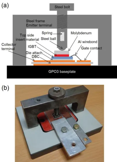
The press pack like single IGBT module samples as shown in Fig.1 were constructed for the electrical tests. The test setup contains two parts, the frame which provides the spring loaded contact and the actual sample. The frame has been designed so that it can be re-used to accommodate a range of test samples. It consists of three parts; a baseplate, a “C” shaped steel frame and a steel bolt. The base-plate is made up of GPO3 which is a composite sheet made up from glass mat and polyester resin. The “C” shaped steel frame is fitted on the top of the base-plate and contains a threaded hole to accommodate a steel bolt. The steel bolt is specially designed with a spring loaded steel ball on one end, which can be moved up and down by turning anticlockwise or clockwise respectively. This steel bolt also acts as the electrical contact for the emitter terminal of the IGBT.
Fig. 1. Press pack like single IGBT module sample for the electrical tests: (a) schematic diagram; and (b) photograph of the sample.
The 13.5mm 13.5mm 0.5mm 2500V/50A corner gate IGBTs were sourced from Dynex Semiconductor Ltd. (Lincoln, UK). They have ~5 m Al metallization on the top emitter and gate pads and ~0.1/1/1 m Ti/Ni/Ag metallization on the collector side. For preparing the test samples, the IGBT was first attached on direct bonded copper (DBC) substrate using either Sn-3.5Ag solder joint or sintered Ag joint for the DA. For
forming the Sn-3.5Ag solder joint, 100 m thick paste (Multicore RM89 96SAAS85V) was first printed on the as-received DBC substrate and put into a furnace preheated at 240 C for 3 minutes. After the sample was taken out of the furnace and cooled down to room temperature, it was ultrasonically cleaned with acetone to remove all visible flux residual surrounding the re-solidified solder pad. Finally, the Sn-3.5Ag solder joint was formed by placing the IGBT on the cleaned solder pad which was re- reflowed in air at a peak temperature of 260 C for 5 minutes. For producing the sintered Ag joint, a layer of ~1 µm thick Ag finish was plated on the surface of the DBC substrate by using brush plating. Either 50 m or 200 m thick preform of Ag nanoparticle was transferred onto the collector side of the IGBT at 130 C for 5 minutes. Then the IGBT with the transferred Ag preform was placed on the DBC substrate with the plated Ag finish, and the final sintering was carried out at a temperature of 250 C and a pressure of 5 MPa for 5 minutes. The as-sintered Ag joint was approximately 25 µm or 100 µm in thickness.
Prior to the overcurrent test, the sample was placed on the base-plate of the frame, where a TSI material was put on the IGBT, followed by an 8 mm 8 mm 2 mm Mo shim on the top (or the Mo shim was directly put on the IGBT without TSI material). For the samples with the Sn-3.5Ag solder joint for the DA, the TSI material (if used) was 8 mm 8 mm 0.5 mm Cu, Sn-3.5Ag, Al or Ag foil, or 8 mm 8 mm 0.1 mm Sn-3.5Ag foil, or 8 mm 8 mm ( 0.05 mm /0.025 mm /0.005 mm) Ag foil. For the samples with the sintered Ag joint for the DA, the TSI material was either 8 mm 8 mm 0.025 mm Ag foil or 8 mm 8 mm 0.1 mm Sn-3.5Ag foil. Results obtained with the Sn-3.5Ag solder joint for the DA were used to inform for the selection of TSI materials for samples with the Ag foil as DA. The sample was loaded under the steel bolt by using a calibrated torque wrench to achieve a specified average pressure of 2 MPa on the TSI/IGBT interface.
B. Electrical Tests
The overcurrent tests were carried out as shown schematically in Fig. 2. A 600V XDC600-20 digital DC power supply made by Xantrex (Burnaby, BC, Canada) was connected to a capacitor bank containing 9 Nippon (Tokyo, Japan) 6.8 mF 400 V aluminium electrolyte capacitors in parallel. An anti-parallel diode was connected across it as a free wheel diode. The positive terminal of the capacitor bank was connected to the collector terminal while the negative terminal of the capacitor bank was connected to the emitter terminal of the IGBT sample.
[image:2.612.69.272.341.621.2]overcurrent tests involve turning on the IGBT into a short circuit causing an uncontrolled flow of current through the device resulting in thermal overload and hence failure. The results associated with the selection of DA and TSI materials should be applicable to other thermal-induced failures of the IGBT accompanying the formation of liquid and gas phases.
After the overcurrent test, collector and emitter terminals of the sample were connected to a 50A/10V or 120A/20V power supply to test the stability of the SCFM. A current of 50 A was selected to pass through the IGBT because it is the maximum average current that can be passed through a single IGBT die under normal conditions. The current through and the voltage drop across the failed IGBT were measured to calculate the resistance. Unless otherwise stated, the test was not stopped until a sample failed to high resistance or the test time reached 150 hours.
C. Structure Characterization
After the current passage test, samples were cross-sectioned, ground and polished for structural characterization. The latter was done using a Hitachi TM3000 scanning electronic microscope (SEM) with a built in energy-dispersive X-ray spectroscopy (EDXS) microanalysis system. For preparing the cross sections samples were first cut using a diamond saw, mounted within an epoxy resin and subsequently ground and polished using 600 grit size SiC paper down to 1 m diamond suspension.
One as-reflowed Sn-3.5Ag solder joint, one as-sintered Ag joint and two representative samples after the electrical tests, one with stable SCFM and one with unstable SCFM, were also characterized using three-dimensional (3D) X-ray computed tomography (CT) imaging, carried out on an Xradia Versa XRM-500 system.
III. FINITE ELEMENT MODELING AND SIMULATION
A. Geometric Model and Meshing System
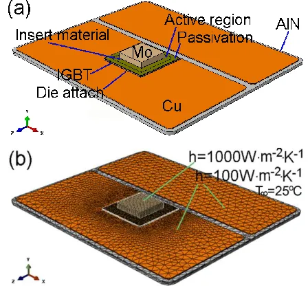
The transient thermal modelling and simulation has been carried out to calculate the temperature fields so as to further verify the formation of liquid and gas phases and compare their volumes in three representative samples during the overcurrent test. This was done using commercial available finite element (FE) analysis software Abaqus 6.14-1 and its graphic user interface CAE. Fig. 3 presents the geometric model and the
meshing system consisting of 197293 elements (D3D8 linear brick elements, DC3D6 linear triangular prism elements and D3D4 linear tetrahedron elements) to discretize the geometric model. The sample frame included in Fig. 1 has been excluded from the model for simplification. This is because during the overcurrent test, the heat transferred to the frame was negligible before the temperatures in the different parts of the actual IGBT sample reached their maximum values.
Non-uniform elements were used to discretize the model. If all the triangle prism elements and tetrahedron elements are imagined as the corresponding brick elements for comparison, the largest element is approximately 2 mm 2 mm 0.56 mm, and the smallest element is 0.25 mm 0.25 mm 0.005 mm. Further refining the meshing system was found to have no substantial effect on the simulation results.
Fig. 3. The FE model used to simulate the temperature fields during overcurrent test: (a) geometric model; and (b) meshing system and boundary condition of heat exchange.
B. Thermal Loads and Boundary Conditions
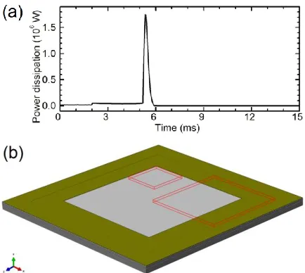
[image:3.612.51.538.50.187.2]The power dissipation described in Fig. 4 was used as the thermal loads during the transient thermal simulation. The curve of power dissipation versus time was obtained from the typical current through and the voltage across the IGBT which were recorded during the overcurrent test. As presented below,
[image:3.612.326.550.406.614.2]one or two craters of 1 to 7 mm in size were found to form under the Mo shim near the corners or edges of the Mo shim within each of the tested samples. Therefore, during the overcurrent test, the heat was probably generating around the original domains of the craters within the active regions of the IGBT devices. For the present purpose of the transient thermal simulation to verify the formation of liquid and gas phases and estimate their volumes, the total power dissipation shown in Fig. 4(a) could reasonably be assumed to equivalently dissipate within two 2.5 mm × 2.5 mm × 0.16 mm and 5.5 mm × 5.5 mm × 0.16 mm active regions of the IGBT as shown in Fig. 4(b). The two active regions were selected because the positions and volumes of the liquid and gas phase determined from the simulation results are in reasonable agreement with those of the observed craters in the corresponding experimentally tested samples.
Fig. 4. Thermal loads applied during the transient thermal simulation: (a) power dissipation by the entire sample; and (b) two active regions of the IGBT enclosed in red lines and assumed to share equivalent amount of power dissipation generating heat.
The heat exchange boundary conditions as also described in Fig. 3(b) were arbitrarily applied to two surfaces of the IGBT sample. A relatively high heat exchange coefficient of 1000 Wm-2k-1 was applied to the top side of the Mo shim taking into account the possible heat transfer through the steel bolt of the sample frame which was ignored in the geometric model. A relatively low heat exchange coefficient of 100 Wm-2k-1 was
applied to the top surface of the DBC substrate describing the boundary condition of air convection. Given the extremely short transient time of 15 ms is it reasonable to assume that within such a short time frame the heat flux would not reach the two surfaces. Changing the heat exchange coefficients or using adiabatic boundary condition were found to have no appreciable effect on the simulation results.
C. Properties of Materials and Simulation Cases
The thermo-physical properties of all the materials for the transient thermal simulation are listed in Table I [14-20]. Rather than using a single melting point and a single boiling point, the “solidus temperature” in combination with “liquidus temperature” and the “boiling temperature 1” in combination with “boiling temperature 2” were employed to model the melting process and boiling process of the different materials. This was to speed up the convergence rate of the transient thermal simulation so as to significantly reduce computation times. Also, for simplification, temperature-independent thermo-physical properties of all the materials were used, the flow of the liquid phases was ignored, but the gas phases were not excluded from the simulation domain after they were formed. These simplifications and assumptions may lead to inaccurate simulation results. However, they are still deemed sufficient for the present purpose to compare the effects of the DA and TSI materials on the volumes of liquid phases and gas phases formed during the overcurrent test.
Three simulation cases considering different combinations of DA and TSI materials were simulated. They are case A with 100 µm thick Sn-3.5Ag solder joint for the DA and 25 µm thick Ag foil for the TSI, case B with 100 µm thick sintered Ag joint for the DA and 25 µm thick Ag foil for the TSI, and case C with 100 µm thick sintered Ag joint for the DA and 100 µm thick Sn-3.5Ag foil for the TSI. These three simulation cases were considered suitable to demonstrate the selection of suitable DA material for achieving stable SCFM. All the three simulation cases were executed on a PC computer with Intel[R] Core[TM] i7-3820 CPU @ 3.60 GHz processor 64 GB RAM. The running times were 12 to 21 hours.
IV. RESULTS AND DISCUSSION
A. Overcurrent Test
[image:4.612.64.281.257.451.2]The overcurrent test was triggered by using a gate drive to turn on the IGBT. After turn on, the IGBT went into the saturation region, where the collector current reached its
TABLE I
THERMO-PHYSICAL PROPERTIES OF ALL MATERIALS FOR THE TRANSIENT THERMAL SIMULATION
Si AlN Cu Mo Ag foil Sintered Ag Al Sn-3.5Ag Passivation
Thermal conductivity (WK-1m-1) 146 175 398 138 429 343 238 33 0.12
Specific heat (J(kg-1C-1) 750 740 380 250 235 235 880 220 1150
Density (gcm-3) 2.33 3.30 8.85 10.22 10.49 8.39 2.7 7.36 1.43
“Solidus temperature” (C) 1414 - 1085 2623 962 962 660 221 -
“Liquidus temperature” (C) 1434 - 1105 2643 982 982 680 241 -
Latent heat of fusion (kJkg-1) 1926 - 205 375 105 105 396 59 -
“Boiling temperature 1” (C) 3265 - 2562 4639 2162 2162 2519 2602 -
“Boiling temperature 2” (C) 3285 - 2582 4659 2182 2182 2539 2622 -
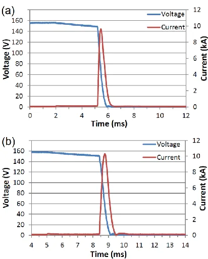
[image:4.612.44.568.614.725.2]Fig. 5. Voltage and current waveforms of two IGBT samples during the overcurrent test: (a) Sn3.5Ag solder joint for the DA and Mo shim directly on the IGBT; (b) Sn3.5Ag solder joint for the DA and 0.5 mm thick Ag for the TSI material on the IGBT.
maximum value and stayed there until the IGBT’s junction temperature exceeded its intrinsic or thermal limits after which device breakdown occurred followed by a sudden influx of current from the capacitor bank. A residual voltage of nearly zero was observed from all samples, indicating that they all failed to SCFM after the overcurrent test at the energy level of 750 J. Fig. 5 presents the waveforms of the recorded currents through and the voltages across the IGBTs of two representative samples during the overcurrent test.
The peak current mainly depended on the TSI material. The highest peak current of 10.33 kA was achieved by using the Ag foil for the TSI material. The lowest peak current of 6.23 kA was achieved by using the Sn-3.5 Ag foil for the TSI material. The peak currents for the Mo (i.e. without any TSI material), Cu and Al TSI materials were 9.63, 9.46 and 7.87 kA respectively. Such a result indicates that a TSI material with a higher activity and/or higher electrical resistivity would lead to a lower peak current. The saturation times of all the samples were very close to each other, in the range 3.15 ms to 3.4 ms. One possible reason for this is that all the samples were very similar in their geometric structure, volume and mass, and the only difference being the use of the different TSI materials.
B. Current Passage Test
As presented in Fig. 6(a), for the samples with the Sn-3.5Ag solder joint for the DA, the Mo based test sample (i.e. Mo directly on IGBT) had an initial resistance of 5.4mΩ, which increased with time until it reached 200mΩ after 33 hours of the current passage test. In addition, the actual final resistance could be much higher as the power supply had been taken into constant voltage mode and thus the test ended up with the
maximum measurable resistance of 200mΩ. Similarly, the Cu based sample had quite low initial resistance of 5.2 mΩ, but also eventually reached 200 mΩ after 18 hours resulting in an unstable short circuit.
In comparison, the resistance of the Sn-3.5Ag TSI based sample was very stable. It started with an initial resistance of 16 mΩ with only negligible change over the 150hr test period indicating stable SCFM.
Fig. 6. Evolutions of resistance during the current passage test for samples with: (a) Sn3.5Ag solder joint for the DA; and (b) sintered Ag joint for the DA.
The Al TSI based sample resulted in initial resistance of 30 mΩ which was significantly higher than the rest of the insert materials. However, the resistance was stable for the initial 17 hours, only decreasing slightly, reaching 23 mΩ after 58 hours where it then stayed unchanged for 92 hours indicating its stability.
The lowest initial resistance was obtained with the Ag TSI based sample. It started at 1.5mΩ and only slightly increased to 1.76 mΩ over the 150 hours. There was no appreciable difference between the samples with 0.5 mm, 0.05 mm and 0.025 mm thick Ag foils for the TSI material. However, if very thin 0.005 mm Ag foil for the TSI material was used, the results of the current passage test had poor repeatability. Results presented either stable SCFM with a resistance of a few mΩ or unstable SCFM with a resistance over 200 mΩ although they all indicated SCFM during the overcurrent test.
[image:5.612.56.262.45.301.2] [image:5.612.329.547.157.467.2]in Fig. 6(b). However, after a relatively short period of time of between 10 to 90 minutes of the current passage test, the resistance values suddenly reduced to 40 to 50 mΩ. For the two samples with the 0.025 mm thick Ag foil for the TSI material, the current passage test was terminated after 2 hour because of emitted gas. The other two samples with 0.1 mm thick Sn-3.5Ag solder foil as the TSI materials lasted for the full 150 hour test duration. However, it can also be seen that their resistance values fluctuated over time and were in the whole clearly higher and more unstable than those of the corresponding samples using Sn-3.5Ag solder joints for the DA. Therefore, all these four samples with the sintered Ag joint for the DA can be considered to have unstable SCFM, or at the very least poor stable SCFM.
It should be pointed out that for the majority of the combination of DA and TSI materials, only one sample has been tested. However, multiple samples have been tested for the Sn-3.5Ag solder joint DA in combination with Ag and Sn-3.5Ag for TSI and sintered Ag joint for the DA in combination with Ag foil for the TSI material. Therefore, the present results of the electrical tests are expected to reflect the effects of the DA and TSI materials on the stability of the SCFM under the current testing conditions.
C. Structure Characterization
As shown in Fig. 7, in a typical as-reflowed Sn-3.5Ag solder joint for the DA, there was a porosity ~1.7%, and size of pores (voids) in the range 40 µm to 575 µm in diameter. For a typical as-sintered Ag joint, there was an “apparent” porosity ~1.5% which was obtained from pores (voids) of 40 µm to 250 µm visible in the reconstructed X-ray CT image. However, a much higher porosity of 30% was determined by measuring the weight and volume of the sintered Ag joint as in the method reported in the existing literature [21].
From the polished cross sections, one or two craters of 1 to 7 mm in size were found to form within the failed IGBT, DA, TSI and Cu layers in each of the samples. The formation of rapid solidification microstructures was common at the interfaces between the IGBT and the residual TSI materials, and on walls of the craters. They included broken small pieces of Si embedded into the matrix which consisted of intermetallic compounds (IMCs) of Mo-Si, Cu-Si, Cu-Sn, dendritic structures of Mo-Si, Cu-Si, and eutectic structures of Mo-Si, Cu-Si, Ag-Si, Al-Si. Table II lists the observed IMCs and alloys, as well as their minimum temperatures of formation, TF, which were derived from the relevant binary phase diagrams [22].
Fig. 7. Reconstructed 3D X-ray CT images taken from : (a) as-reflowed Sn-3.5Ag solder joint; (b) as-sintered Ag joint.
TABLE II
THE IMCS AND ALLOY WHICH WERE OBSERVED TO BE DIRECTLY IN CONTACT WITH THE TSI MATERIALS IN THE TESTED SAMPLES
TSI material IMCs Alloys TF (C)
Mo MoSi2 - 1947
Cu Cu33Si7, Cu15Si4, Cu19Si6 - 1127
Sn-3.5Ag - Small Si particles in Sn-3.5Ag 1177
Al - Al 60 at% Si 40 at% 1147
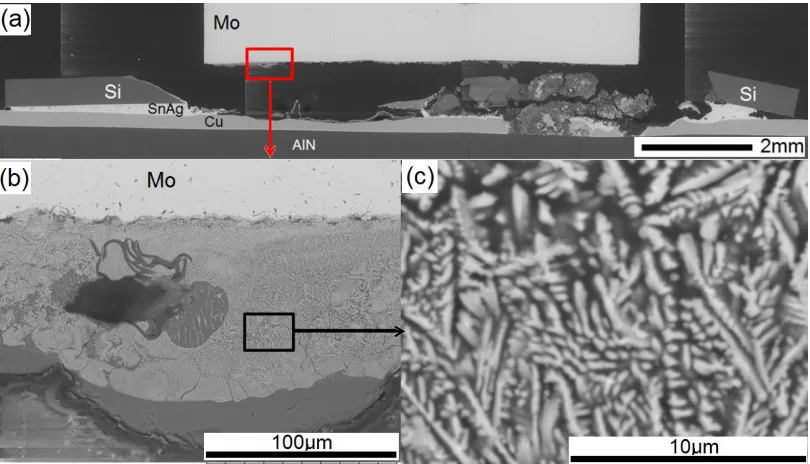
Fig. 8. SEM image taken from the sample with Sn-3.5Ag solder joint for the DA and Mo shim directly in contact with the IGBT: (a) overview; (b) enlarged view showing the dendrite structure; (c) further enlarged view showing detail of the MoSi2 dendrites.
Fig. 9. SEM image taken from the sample with Sn-3.5Ag solder joint for the DA and 0.5 m thick Ag foil for the TSI material: (a) overview; (b) enlarged view showing a conductive channel; (c) further enlarged view showing Si dendrites filled with conductive Ag network.
If the Sn-3.5Ag solder joint was used for the DA, the formation of Cu6Sn5 and Cu3Sn IMCs was observed at the solder-DBC substrate interface. Sn-3.5Ag solder was also observed to fill in the cracks within failed Si IGBT and connect to the top side solidification microstructures. If the sintered Ag joint was used for the DA, a hypo-eutectic structure consisting of black phase Si and white phase Ag plus minor Cu and Al and having a thickness of tens of micron was found to cover the walls of the craters within the failed Si IGBT and near the sintered Ag joint.
Figures 8 and 9 show representative cross-sectional SEM images taken from two samples after the current passage test. It
can be seen that for the sample with the Mo shim directly in contact with the top side of the IGBT, the rapid solidification structure under the Mo shim has been broken into pieces and the effective connection between the Mo shim and the Cu layer of the DBC substrate has almost been lost. By contrast, for the sample with the Ag insert material, the structure integrity of the rapid solidification structure was intact and the effective connection between the Mo shim and Cu layer of the DBC substrate still remains.
Fig. 10. Reconstructed 3D X-ray CT images taken from the samples with Sn-3.5Ag solder joint for the DA and 25 m thick Ag foil for the TSI material: (a) one cross-sectional view, (b) 3D overview; and sintered Ag joint for the DA and 100 m thick Sn-3.5Ag foil for the TSI material: (c) one cross-sectional view; (d) 3D overview.
particular, sufficient amount of highly conductive phase passing through the failed IGBT and connecting to the top side Mo shim and bottom side Cu layer of the DBC substrate can also be observed. In the sample with the sintered Ag joint for the DA, it is hard to see the craters formed within the Si IGBT, DA and Cu layer of the DBC substrate. This is due to the insufficient contrast of the images caused by the shadow effect of Mo shim with intensive absorption to the X-ray on the top side and the lack of phase/material with sufficient absorption to the X-ray within the focused layers. Nevertheless, it can be noted that the amount of highly conductive phase passing through the failed IGBT was very low.
D. Transient Thermal Simulation
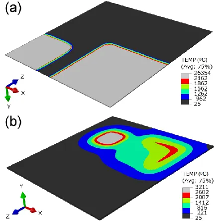
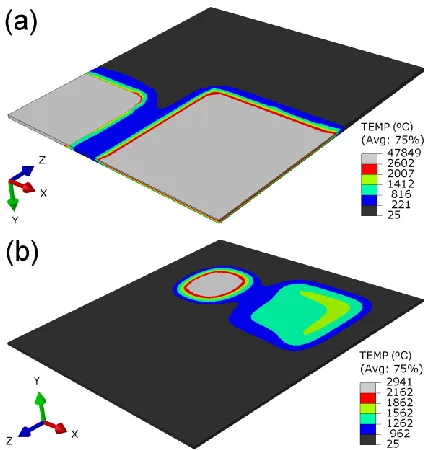
Figures 11 and 12 present the transient thermal simulation results of temperature fields within the TSI and DA of simulation cases A and C, respectively. In both figures, the domains shown in blue to red have temperatures between the “solidus temperatures” and “boiling temperature 1” (see table 1) and hence stand for the volumes of the liquid phases. The domains shown in white have temperatures above “boiling temperature 1” or “boiling temperature 2” (being similar in value) and hence stand for the volumes of the gas phases. For the simulation case B, the volumes of liquid phase and gas phase within the TSI of 25 µm thick Ag foilare similar to those shown in Fig. 11(a), and the volumes of the liquid phase and gas phase within the DA of 100 µm thick sintered Ag joint are similar to those shown in Fig. 12(b). Therefore, it can be seen that the gas phases could indeed be formed within both the DA and TSI materials for all the three simulation cases. Using Sn-3.5Ag foil can somewhat increase the volume of liquid phase than using Ag foil for the TSI material, while using Sn-3.5Ag solder joint can significantly increase the volume of liquid phase than using the sintered Ag joint for the DA material. This can be readily attributed to the fact that the
[image:8.612.65.281.44.669.2] [image:8.612.329.544.478.700.2]Fig. 12. Transient thermal simulation results of case C, showing the largest volumes of the liquid phases (in blue to red) and gas graphs (in white) within: (a) TSI, 100 Sn-3.5Ag solder foil; and (b) DA, 100 µm thick sintered Ag joint.
Sn-3.5Ag solder joint and foil have much lower melting points (“solidus temperature” in Table I) and much higher boiling point (“boiling temperature 1” in Table I) than the Ag foil or sintered Ag joint.
E. Discussion
The revelation of the rapid solidification structure in all the tested samples verifies the formation of liquid during the overcurrent test. Electrical arc and explosion observed during the overcurrent test further confirms the production of a certain amount of high temperature gas. This was further supported by the transient thermal simulation results. Therefore, the formation of the craters within the failed Si IGBT, DA, TSI and Cu layers of the DBC substrate in all the tested samples can be attributed to material removal in the form of gases and liquids distributed by the explosion.
In the rapid solidification structure, the IMCs of Mo-Si, Cu-Si, Cu-Sn, and the metallic Mo, Cu, Ag, Al in dendritic structures of Mo-Si, Cu-Si and eutectic structures of Mo-Si, Cu-Si, Ag-Si, Al-Si have relatively high electrical conductivities allowing the formation of conductive networks passing through the failed IGBT and connecting to the Mo shims and the Cu layers of the DBC substrates in samples after the overcurrent test. Furthermore, the loaded spring kept applying pressure and bringing the emitter electrode back in contact with the failed IGBT. Therefore, all the samples resulted in SCFM during the overcurrent test under the energy level of 750 J which can meet realistic applications [12].
The voids in the as-reflowed Sn-3.5Ag solder joint and the as-sintered Ag joint visible in the reconstructed X-ray CT images are significantly more in number and smaller in size than the craters formed during the overcurrent test. These voids could reduce the thermal conductance to some extent, but should not have an appreciable effect on the electrical
conductance for the DA layers in all the samples. Therefore their effects on the results of the electrical tests were deemed secondary and negligible. On the other hand, the craters were observed to form under the Mo shim near one corner or one edge of the Mo shim in all the samples after the overcurrent test. Due to the spring steel bolt, the pressure is maximum (~11 MPa estimated with FE simulation) at the central point of the IGBT, and “parabolically” reduced to zero under the corners and edges of the Mo shim. Therefore, the thermal-induced short circuit failure was probably initiated and developed near the corner or edge because of relatively high electrical contact resistance between the IGBT and Mo shim caused by the relatively low pressure.
Comparing the samples using the sintered Ag joint for the DA with those samples using the Sn3.5Ag joint for the DA, the amount of liquid formed in the DA layers in the former samples was significantly less than that in the latter samples. As a result, no molten or re-solidified Ag was detected in the cracks within the failed Si IGBT, and the amount of the conductive Ag in the solidification structure was quite low. This might lead to relatively high resistance, poor alignment/connection between the Mo shim and the failed IGBT, causing locally high thermal expansion and frequent re-alignment and hence the variation/fluctuation in the resistance during the current passage test. This is probably the main reason why the samples using the sintered Ag joint for the DA had unstable or poor stable SCFM during the current passage test.
In the samples where Mo and Cu were used for the TSI material, the alignment between the IGBT and the TSI material was relatively poor. Such an arrangement led to the development of small and localized conductive/contact paths which resulted in low initial resistance. Later during the current passage test, these small conductive paths were unable to support 50A of current for a long time and hence this resulted in an unstable SCFM. On the other hand, The MoSi2, Cu33Si7, Cu15Si4 and Cu19Si6 IMCs formed at that interfaces were very brittle and scarcely connected to the failed IGBTs. Therefore, during the current passage test, the initial resistance was low but as soon as the sample started heating up, the IMCs being hard, could not realign well and hence also contributed to an unstable SCFM.
By contrast, in the samples where Sn-3.5Ag, Al and Ag were used for the TSI material, there was the formation of Sn-3.5Ag channels through the cracks within the failed Si IGBTs. There was also less probability for the formation of the broken pieces of Si without any conductive material between them. From both these observations it can be inferred that the active contact area between the TSI material and the IGBT was much better than those in the samples where the Mo and Cu was used. Because of the large contact area, the overall resistance was low which resulted in lower power dissipation during both the overcurrent test and the current passage test. Therefore, the chances of the formation of local hotspots were low which helped in the stability of the low resistance throughout the tests.
[image:9.612.65.278.47.272.2]materials. This is probably because the Al is very reactive, and there is always a very thin and dense layer of Alumina (around 10 nm) once Al is exposed to air. The Alumina which is a very good insulator even if it is very thin may have contributed to the increase in contact resistance. Another possibility is the poor wettability of liquid Al because of surface oxides which resulted in reduction in the true contact area between the Al and the IGBT.
Despite that larger volume of liquid could be formed when using the Sn-3.5Ag foil than using the Ag foil for the TSI material, most of the liquid could be intensively disturbed and removed away by the explosion because the liquid formed was directly in contact with the active regions and heat sources of the IGBT during the overcurrent test. On the other hand, Sn-3.5Ag solder alloy has much lower electrical conductivity than Ag. These should be reason why the sample with the Sn-3.5Ag for the TSI material had higher resistance than the samples with the Ag foils for the TSI material during the current passage test. Ag foils for the TSI material resulted in the lowest contact resistance because Ag is the best electrical conductor, less reactive and very compliant. The poor repeatability from the samples using 0.005 mm thin Ag insert material can simply be ascribed to the fact that such a thin layer of insert material can easily lead to poor alignment between the Mo shim and the failed IGBT.
V. CONCLUSION
When Mo is directly put on the IGBT, the SCFM obtained from the reaction between Mo and molten Si is unstable. Thus, further experimentation is needed to investigate the reported SCFM of the PPIM based on packaging technology of the press pack thyristor modules [3].
Using Cu foil for the TSI material, the SCFM obtained is unstable. Using sintered Ag joint for the DA in combination with Ag or Sn-3.5Ag foil for the TSI material, the SCFM is also unstable. These results do not support the recommendations in [6] that sintered Ag joints could be used for the DA, and Cu could be used for the TSI.
Using Sn-3.5Ag solder joint for the DA, stable SCFM is achieved with Sn-3.5Ag, Al and Ag foil for the TSI material. The best result is obtained with the Ag foil, and a layer of 25 m thick Ag foil on 0.5 mm thick Si IGBT is sufficient to produce stable SCFM. This reveals that the thickness of the TSI material is not needed to be at least half of the IGBT thickness as given in [6].
The microstructure containing sufficient amounts of highly conductive phases to form conductive networks / channels through the failed IGBT while having good alignment between the top side Mo shim and the failed IGBT or the Cu layer of the DBC substrate would appear to favor stable SCFM.
The transient thermal simulation results can be used to not only further verify the formation of liquid phases and gas phases during the overcurrent test, but also correlate the stable and unstable SCFM with volumes of the liquid phases formed in the different samples.
REFERENCES
[1] J. Bing, X. Song, E. Sciberras, W. Cao, Y. Hu, and V. Pickert,
“Multiobjective design optimization of IGBT power modules considering power cycling and thermal cycling” IEEE Trans. Power Electron. , vol. 30, no. 5, pp. 2493–2504, Feb. 2015.
[2] F. Wakeman, W. Findlay, and G. Li, "Press-pack IGBTs, semiconductor switches for pulse power," in Pulsed Power Plasma Science, 2001. PPPS-2001. Digest of Technical Papers, vol. 2, pp. 1051-1054, June 2001.
[3] An application note for possible failure modes in press pack devices. Available from the website: www.westcode.com/app_note/2012an04. pdf, 2002.
[4] S. Eicher, M. Rahimo, E. Tsyplakov, D. Schneider, A. Kopta, U. Schlapbach, and E. Carroll, “4.5kV press pack IGBT designed for ruggedness and reliability,” in Industry Applications Conference, 2004. 39th IAS Annual Meeting, Conference Record of the 2004 IEEE, vol. 3, pp.
1534-1539, 2004.
[5] S. Gunturi and D. Schneider, “On the operation of a press pack IGBT module under short circuit conditions” IEEE Trans. Adv. Pack., vol. 29, no. 3, pp. 433-440, Aug. 2006.
[6] C. Liu, N. Schulz, and S. Kicin, “Power semiconductor module and method of manufacturing a power semiconductor module,” US patent, US2012211799A1, Aug. 23, 2012.
[7] F. Wakeman, K. Billett, R. Irons and M. Evans, “Electromechanical characteristics of a bondless pressure contact IGBT," in Applied Power Electronics Conference and Exposition, 1999, APEC'99, Fourteenth Annual, vol. 1, pp. 312-317, March 1999.
[8] M. J. Evans, "Pressure contacted IGBTs," in Recent Advances in Power Devices (Ref. No. 1999/104), IEE Colloquium on, 1999, pp. 7/1-7/5, June 1999.
[9] F. J. Wakeman, and G. W. Lockwood, "Electromechanical evaluation of a bondless pressure contact IGBT," in Circuits, Devices and Systems, IEE Proceedings, vol. 148, pp. 89-93, April, 2001.
[10] S. Gunturi, J. Assal, D. Schneider, and S. Eicher, "Innovative metal system for IGBT press pack modules," in Power Semiconductor Devices and ICs, 2003. Proceedings. ISPSD '03. 2003 IEEE 15th International
Symposium on, pp. 110-113, August 2003.
[11] S. Eicher, M. Rahimo, E. Tsyplakov, D. Schneider, A. Kopta, U. Schlapbach, and E. Carroll, "4.5kV press pack IGBT designed for ruggedness and reliability," in Industry Applications Conference, 2004. 39th IAS Annual Meeting. Conference Record of the 2004 IEEE, vol. 3, pp. 1534-1539, October 2004.
[12] I. Yaqub, J. F. Li, and C. M. Johnson, “Dependence of overcurrent failure modes of IGBT modules on interconnect technologies,” Microelectron. Reliab., vol. 55, no. 12, Part A, pp. 2596-2605, Dec. 2015.
[13] J. F. Li, I. Yaqub, and C. M. Johnson, “Selection of materials for IGBT modules to achieve stable short circuit failure behaviour,” In: PCIM Asia 2016 - International Exhibition and Conference for Power Electronics, Intelligent Motion, Renewable Energy and Energy Management, 28-30 June 2016, Shanghai, China. pp. 58-65.
[14] A. Zéanh, O. Dalverny, M. Karama, E. Woirgard, S. Azzopardi, A. Bouzourene1, J. Casutt, and M. M. Guyennet, “Thermomechanical Modelling and Reliability Study of an IGBT Module for an Aeronautical Application,” in Proceedings of 9th Int. Conf. on Thermal, Mechanical
and Multiphysics Simulation and Experiments in Micro-Electronics and Micro-Systems, EuroSimE 2008, Freiburg-im-Breisgau, Germany, April 21-23, 2008.
[15] A. Zeanh, O. Dalverny, M. Karama, and A. Bouzourene, “Lifetime and reliability assessment of AlN substrates used in harsh aeronautic environments power switch modules,” Advanced Materials Research, vol. 112, pp 113-127, May 2010.
[16] J. G. Bai, Z. Z. Zhang, J. N. Calata, and G. Q. Lu,” Thermomechanical Reliability of Low-Temperature Sintered Silver Die Attached SiC Power Device Assembly,” IEEE Trans. Device Mater. Reliab.,vol. 6, no. 3, pp. 436-441, Sept. 2006.
[17] W.W. Sheng and R.P. Colino, Power Electronic Modules: Design and Manufacture, CRC Press LLC, Florida, USA, 2005.
[18] Melting and Boiling Temperatures - Evaporation and Melting Heats common Materials. Available from the website: http://www. engineeringtoolbox.com/melting-boiling-temperatures-d_392.html [19] Metals – Latent Heat of Fusion. Available from the website:
http://www.engineeringtoolbox.com/fusion-heat-metals-d_1266.html [20] Metals – Latent Heat of Evaporization. Available from the website:
http://www.engineeringtoolbox.com/fluids-evaporation-latent-heat-d_ 147 . html
time, temperature and pressure on density, strength and reliability” in
Proceedings of CIPS 2010, 6th International Conference on Integrated
Power Electronics Systems, Nuremberg, Germany, paper 10.3, March
16-18, 2010.
[22] SGTE Alloy Phase Diagrams. Available from the website: http://www.crct.polymtl.ca/fact/ documentation/SGTE/SGTE_Figs.htm
Jianfeng Li received the B.S. degree in mineralogy from Nanjing University, Nanjing, China, in 1991, and the M.S. and Ph.D. degrees both in materials science from the Shanghai Institute of Ceramics, Chinese Academy of Sciences, Shanghai, China, in 1996 and 1999, respectively. He worked in the areas of thermal spray, laser materials processing, and high-temperature electronic packaging at the University of Technology of Belfort, Monbeliard, France, the University of Manchester, and King’s College, London, U.K., until 2007. He joined the Power Electronics, Machines and Control Group of the University of Nottingham in the UK in 2008. He is currently a Senior Research Fellow, and working in integration, packaging, thermal, electro-thermal and thermo-mechanical simulation, new packaging structure, manufacturing technologies and reliability of high performance and low cost power electronic modules.
Imran Yaqub received his BSc degree in Electrical Communication from University of Engineering and Technology Taxila, Pakistan, MSc degree in Power Electronics and Control Systems from University of Bradford, UK and PhD degree in Electrical Engineering from University of Nottingham, UK in 2004, 2009 and 2015 respectively. From 2009 to 2011 he worked as a Knowledge Transfer Partnership Associate at the University of Nottingham working along with its industrial partner Dynex Semiconductor Ltd, UK, where he was involved in the design and development of automated test system for high power semiconductor devices. He currently works as a senior Power Systems Engineer at Dynex Semiconductor Ltd, UK, where he deals with many technical aspects of a system design e.g. electrical, thermal, electro-magnetic and control to construct high power converters and inverters.
Martin Corfield (no photo available) received the BSc. degree in Engineering Science from the University of Hull, Kingston upon Hull, U.K. in 1996, and Mphil and Ph.D. degrees in Metallurgy and Materials from the University of Birmingham, Birmingham, U.K. in 1998 and 2003 respectively. He has held research fellowship posts with the University of Birmingham and the University of Sheffield, Sheffield, U.K. He currently holds the position of Research Fellow within the Department of Electrical and Electronic Engineering at the University of Nottingham, Nottingham, U.K.